Yuchen Gao, Yu Ye. Interaction of moiré excitons with cavity photons in two-dimensional semiconductor hetero-bilayers[J]. Journal of Semiconductors, 2023, 44(1): 011903
Search by keywords or author
- Journal of Semiconductors
- Vol. 44, Issue 1, 011903 (2023)
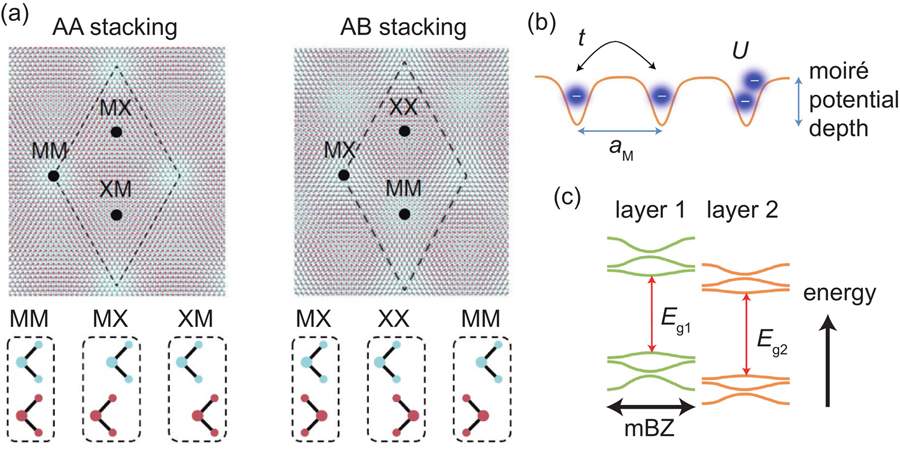
![(Color online) Moiré lattice. (a) Moiré lattice structure for AA-stacked and AB-stacked TMD semiconductors (top). The high-symmetry sites for each case are labelled; their cross-section views are shown (bottom). The large and small dots label the transition metal atom (where M is Mo and W) and the chalcogen atom (where X is S, Se and Te), respectively. (b) Schematic illustration of an array of moiré atoms that trap electrons, which can tunnel between neighboring sites with amplitudet and experience on-site Coulomb repulsionU. (c) Schematic layer-resolved moiré band structure for semiconductor moiré materials with type-II band alignment. mBZ stands for mini-Brillouin zone, andEg1 andEg2 are the bandgap of the first and second TMD layers, respectively[6].](/richHtml/jos/2023/44/1/011903/jos_44_1_011903_f1.jpg)
Fig. 1. (Color online) Moiré lattice. (a) Moiré lattice structure for AA-stacked and AB-stacked TMD semiconductors (top). The high-symmetry sites for each case are labelled; their cross-section views are shown (bottom). The large and small dots label the transition metal atom (where M is Mo and W) and the chalcogen atom (where X is S, Se and Te), respectively. (b) Schematic illustration of an array of moiré atoms that trap electrons, which can tunnel between neighboring sites with amplitudet and experience on-site Coulomb repulsionU. (c) Schematic layer-resolved moiré band structure for semiconductor moiré materials with type-II band alignment. mBZ stands for mini-Brillouin zone, andEg1 andEg2 are the bandgap of the first and second TMD layers, respectively[6].
![(Color online) Moiré exciton in a FP cavity. (a) Cavity setup at 4.2 K: the fiber-based micro-mirror forms the cavity together with a planar macro-mirror with CVD-grown MoSe2–WSe2 heterostructure on top. Independent translational degrees of freedom enable lateral sample displacement and cavity length detuning. (b) Spectra of interlayer exciton PL for the corresponding cavity lengths. (c) Traces of interlayer exciton PL decay shown for three selected cavity lengths of 35, 17, and 6μm. The solid lines are fits to the data with three-exponential decay constants. Note the speed up in the decay upon the reduction of the cavity length[19].](/richHtml/jos/2023/44/1/011903/jos_44_1_011903_f2.jpg)
Fig. 2. (Color online) Moiré exciton in a FP cavity. (a) Cavity setup at 4.2 K: the fiber-based micro-mirror forms the cavity together with a planar macro-mirror with CVD-grown MoSe2–WSe2 heterostructure on top. Independent translational degrees of freedom enable lateral sample displacement and cavity length detuning. (b) Spectra of interlayer exciton PL for the corresponding cavity lengths. (c) Traces of interlayer exciton PL decay shown for three selected cavity lengths of 35, 17, and 6μm. The solid lines are fits to the data with three-exponential decay constants. Note the speed up in the decay upon the reduction of the cavity length[19].
Fig. 3. (Color online) Hybrid moiré exciton in a FP cavity. (a) Resonantly enhanced interlayer hybridization of TMD double layers can result from interlayer charge hopping (blue arrows) in conduction bands for certain combinations of TMDs. Such band alignment yields nearly degenerate intra- and interlayer exciton species (red arrows)[21]. (b) Top, theoretical optical absorption spectrum calculated from the moiré exciton band structure. Bottom, reflection contrast spectra near the MoSe2 A-exciton resonance, from the WS2–MoSe2 hetero-bilayer (red), MoSe2 monolayer and WS2 monolayer (green). The MoSe2 monolayer A-exciton (XA) splits into two well resolved moiré excitons (X1 and X2) in the hetero-bilayer. (c) Angle-resolved white-light reflection spectra, demonstrating strong coupling between moiré excitons and cavity photon at 5 K. The left and right panels show the measured and simulated results, respectively. (d–f) Shift of exciton energy ΔE, half-linewidthγ, and normalized coupling strengthΩ/Ω0 of the hetero-bilayer LPs (red) and monolayer LPs (blue) as a function of carrier density. The hetero-bilayer ΔEhBL-X andγhBL-X (red circles in (d, e)) are approximately constant. The monolayer ΔEML-X andγM-X (blue diamonds in (d, e)) are fitted by a second-order polynomial and a linear fit, respectively (black solid lines in (d, e)). In (f), the black lines and black dashed line are fitting results[20].
Fig. 4. (Color online) Novel theory prediction of moiré exciton in a cavity. (a) The three lowest bands of the spin-up moiré interlayer exciton with a 5 nm moiré period. The moiré potential leads to three well-separated eigenmodesB↑,A↑ andC↑ at Γ, which have σ–, σ+ andz-polarized optical dipoles, respectively. (b) The gradient of an interlayer bias introduced by a split gate can apply an in-plane forceF on the interlayer exciton. (c) Illustration of the polarization Hall effect driven byF. (d) Scattering induced polarization currents under excitation at given energy-momentum points (empty dots) in the LP and UP branches. Cavity photon lifetime is taken as 1 ps[22].

Set citation alerts for the article
Please enter your email address


