
Congyu Hu, Katsuhiko Saito, Tooru Tanaka, Qixin Guo. Growth properties of gallium oxide on sapphire substrate by plasma-assisted pulsed laser deposition[J]. Journal of Semiconductors, 2019, 40(12): 122801
- Journal of Semiconductors
- Vol. 40, Issue 12, 122801 (2019)
Abstract
1. Introduction
Gallium oxide (Ga2O3) has recently attracted attention from the science community due to its interesting properties such as good thermal stability, high dielectric constant, and wide bandgap[
We have systematically investigated the substrate temperature effect on the structural and optical properties of the β-Ga2O3 films on a (0001) sapphire substrate grown by PLD and revealed that (
2. Experiment
Gallium oxide films were grown on a (0001) sapphire substrate with a homemade oxygen plasma-assisted PLD system which has a growth chamber, an oxygen plasma source and a KrF excimer laser (λ = 248 nm) with a frequency of 2 Hz and energy of 225 mJ/cm2. The oxygen plasma cell was surrounded by a helical RF (13.56 MHz) coil. The sapphire substrate was ultrasonically cleaned in methanol for 20 min and again in acetone for 20 min. Then, the substrate was etched in a hot acidic solution H3PO4 : H2SO4 (1 : 3) for 5 min to remove residual oxides on the surface. Finally, it was rinsed with deionized water and followed by N2 blow drying before the substrate was introduced into the growth chamber. Facing the substrate, a 99.99% pure Ga2O3 ceramic disk was set as the target. Prior to deposition, the growth chamber was evacuated to pressure below 5 × 10⁻⁶ Pa with a turbo molecular pump. High purity oxygen gas (99.999%) was then introduced into the oxygen plasma cell through a mass flow controller. The oxygen pressure used in this work was kept at 0.01 Pa and substrate temperature was kept at 500 °C while applied RF power was varied from 0 to 300 W. The growth time was 180 min for all samples.
After growth, the thickness of the films were determined by a step profile analyzer. The structural properties of the films were characterized by X-ray diffraction (XRD) (Cu anode, Kα line, λ = 1.54 Å). Raman measurements were performed on a Horiba Jobin Yvon LabRAM HR 800 system with an Ar laser operating at a wavelength of 488 nm as the excitation source at room temperature. Optical transmittance spectra were measured by a UV-vis spectrophotometer. Surface morphology and roughness of the films were determined by an atomic force microscope (AFM).
3. Results and discussion
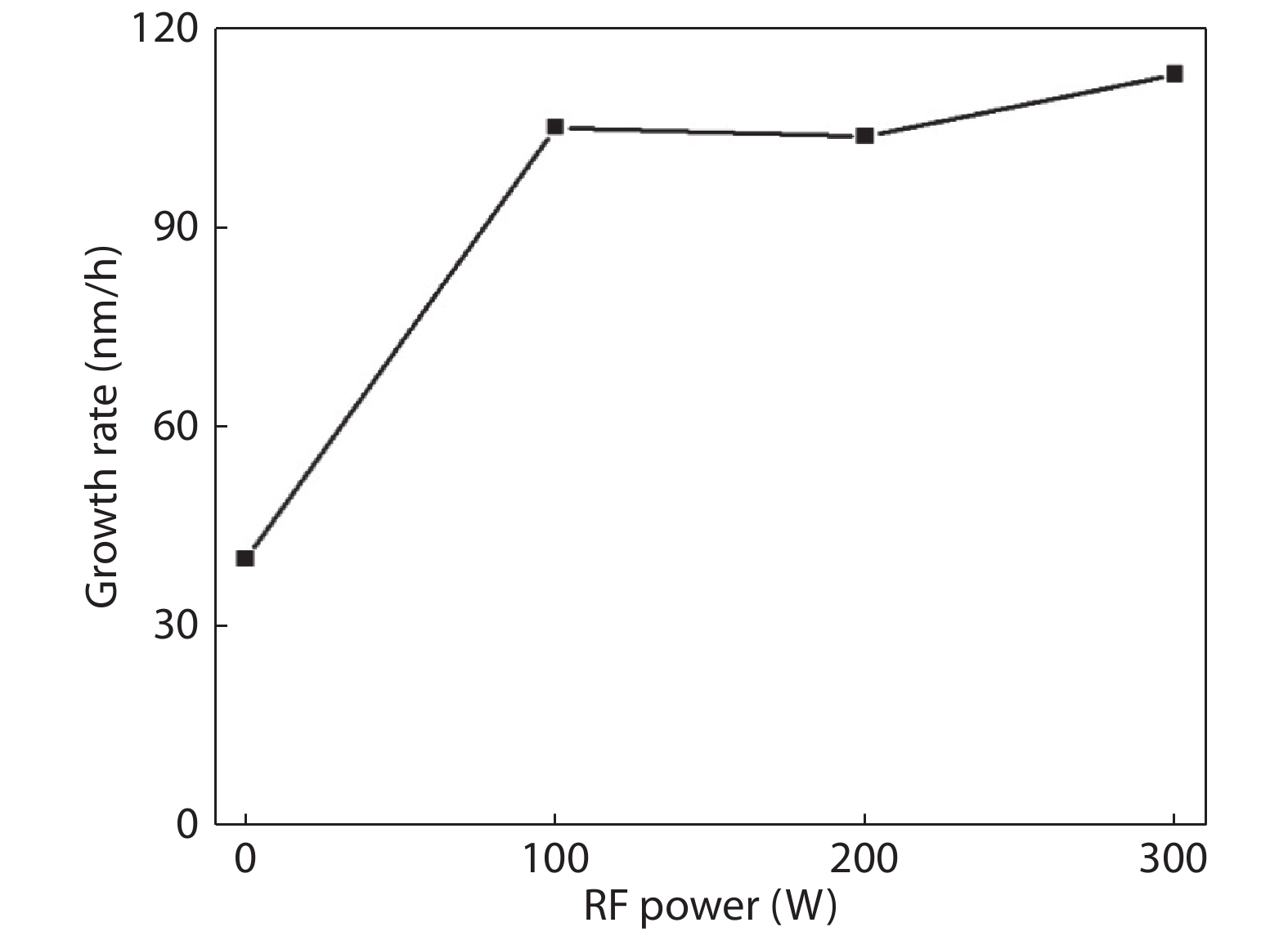
Fig. 1 shows the dependence of film growth rate for β-Ga2O3 on RF power at 500 °C. Film grown in plasma generated oxygen radical background shows significant increase in growth rate compared to film grown in non-reactive O2 ambient. The growth rate of film in oxygen radical background was 2.7 times faster than film grown in non-reactive oxygen ambient (at 0.01 Pa). The 100 and 200 W samples had similar growth rate of 105 and 104 nm/h, respectively and the 300 W sample grew only slightly faster at 113 nm/h. In other words, increasing RF power of the plasma source made a small increase to film growth rate.
![]()
Figure 1.Dependence of growth rate of film on plasma RF power ranged from 0 to 300 W at substrate temperature of 500 °C.
XRD patterns of θ–2θ scan for the samples fabricated with different RF power are shown in Fig. 2. All samples showed diffraction peaks at 18.9°, 38.2°, 58.9°, and 82.0° and by comparing these peaks to data in the International Center for Diffraction Data catalog, these peaks correspond to (
![]()
Figure 2.XRD 2
Raman spectra, shown in Fig. 3, are obtained at room temperature for β-Ga2O3 films fabricated at different RF power to confirm the crystal structure. Raman spectroscopy identifies vibrational mode in a crystal structure. Raman shift peaks were identified for all samples ranging from 100 to 1000 cm−1. For the 100 W sample, peaks were observed at 144, 167, 198.5, 350.4, 470, 652.6, and 767.8 cm−1 and assigned to phonon mode of Bg(2), Ag(2), Ag(3), Ag(5)/Bg(3), Ag(7)/Bg(4), Ag(9)/Bg(5), and Ag(10), respectively by comparing these peaks to the data of bulk monoclinic β-Ga2O3[
![]()
Figure 3.Raman scattering spectra of samples prepared at substrate temperature of 500 °C and power ranged from 0 to 300 W.
Table Infomation Is Not EnableThe transmittances of the films, shown in Fig. 4, were above 80% in the visible and UV regions and sharp absorption edges were observed around wavelength of 250 nm for all the films grown in ambient oxygen radical. In addition, absorption edge of the samples with plasma treatment are steeper than the adsorption edge of the sample without plasma treatment but this is because the thickness of the films are not the same.
![]()
Figure 4.(Color online) Transmittance of films fabricated at fixed substrate temperature of 500 °C but RF power ranged from 0 to 300 W.
Fig. 5 shows morphology of samples by AFM. The surface morphology of sample without plasma treatment showed column shaped crystallites. This is a sign of typical island growth. Samples with plasma treatment also showed column shaped crystallites. The columns in AFM image of samples with plasma treatment are finer, denser, and trenches in between columns are shallower as applied RF power increases. it is also shown in Fig. 6 that the root mean squared (RMS) roughness of samples with higher RF power treatment is much lower than the samples with lower RF power plasma treatment or no treatment. In addition, the RMS roughness for samples with plasma treatment appears to decrease linearly with respect to the RF power applied.
![]()
Figure 5.(Color online) Surface morphology of Ga2O3 film at 0.01 Pa and at (a) 500 °C, 0 W; (b) 500 °C, 100 W; (c) 500 °C, 200 W; (d) 500 °C, 300 W on a 10 × 10
![]()
Figure 6.Dependence of root-mean-squared surface roughness of Ga2O3 film on RF power ranged from 0 to 300 W at fixed substrate temperature of 500 °C.
As shown from the above results, plasma treated samples show a significant increase of heteroepitaxial growth without losing crystallinity compared to a film without plasma treatment. One possible explanation is that crystallization growth of β-Ga2O3 follows the metal-insulator transition mechanism as proposed by Nagarajan et al.[
When plasma treatment was not applied, the deficiency of oxygen atom near the surface makes it much more likely to form the gaseous, volatile gallium suboxide, such as Ga2O. This process was repeatedly reported in several studies of Ga2O3 growth in MBE process[
The AFM images in Fig. 5 and roughness of surface relationship with applied RF power in Fig. 6 showed some insight of the effect of increased RF power. It is speculated that higher RF power results in more nucleation sites. As shown in Fig. 5, the crystallites are tall and big in the film grown without plasma treatment because the nucleation sites are scattered sparsely. Therefore, there is enough space for the crystallites to grow large and tall. However, as the RF power increase, the density of crystallites columns increases. This indicates that as RF power increases, more nucleation sites are available. The same amount of arriving species had to be shared by more nucleation sites. As a result, each crystallite is small and short and the roughness of sample at higher RF power showed smaller surface roughness.
4. Conclusion
Monoclinic β-Ga2O3 films were fabricated by oxygen plasma-assisted PLD method. A film grown in oxygen radical ambient is 2.7 times thicker than films grown in non-reactive O2 background. Increasing strength of RF power showed small increase on growth rate of monoclinic β-Ga2O3 film. XRD and Raman spectroscopy verified that β-Ga2O3 films grown in oxygen radical ambient at 500 °C. The film also showed typical island growth and film grown at higher RF power showed a smoother surface than film grown at lower RF power or no plasma. Transmittance of these films is at least 80% and shows sharp absorption edge at 250 nm. It is speculated that a higher film growth rate in the reactive case is because monoatomic oxygen can migrate deep into the as-deposited film to support Ga2O3 formation and ease the excess concentration of Ga atom near the surface so that Ga2O formation is mitigated. Further research by manipulating oxygen pressure and laser pulse setting should change the crystalline quality and growth rate. In addition, using an oxygen isotopic tracer to study the concentration of background oxygen atom in Ga2O3 would help to reveal the the mechanisms of Ga2O3 heteroepitaxial growth.
Acknowledgements
This work was partially supported by the Scientific Research (No. 16K06268) and the Partnership Project for Fundamental Technology Researches of the Ministry of Education, Culture, Sports, Science and Technology, Japan.
References
[1] C Y Huang, R H Horng, D S Wuu et al. Thermal annealing effect on material characterizations of
[2] R Roy, V G Hill, E F Osborn. Polymorphism of Ga2O3 and the system Ga2O3–H2O. J Am Chem Soc, 74, 719(1952).
[3] L Binet, D Gourier. Origin of the blue luminescence of
[4] Y Kokubun, K Miura, F Endo et al. Sol-gel prepared
[5] T Oshima, T Okuno, N Arai et al. Vertical solar-blind deep-ultraviolet schottky photodetectors based on
[6] M Orita, H Ohta, M Hirano et al. Deep-ultraviolet transparent conductive
[7] M Orita, H Hiramatsu, H Ohta et al. Preparation of highly conductive, deep ultraviolet transparent
[8] M Higashiwaki, K Sasaki, T Kamimura et al. Depletion-mode Ga2O3 metal-oxide-semiconductor field-effect transistors on
[9] S A Lee, J Y Hwang, J P Kim et al. Dielectric characterization of transparent epitaxial Ga2O3 thin film on n-GaN∕Al2O3 prepared by pulsed laser deposition. Appl Phys Lett, 89, 182906(2006).
[10] K Matsuzaki, H Yanagi, T Kamiya et al. Field-induced current modulation in epitaxial film of deep-ultraviolet transparent oxide semiconductor Ga2O3. Appl Phys Lett, 88, 092106(2006).
[11] T Oshima, T Okuno, S Fujita. Ga2O3 thin film growth on
[12] T Oshima, N Arai, N Suzuki et al. Surface morphology of homoepitaxial
[13] F B Zhang, K Saito, T Tanaka et al. Structural and optical properties of Ga2O3 films on sapphire substrates by pulsed laser deposition. J Cryst Growth, 387, 96(2014).
[14] M Fleischer, W Hanrieder, H Meixner. Stability of semiconducting gallium oxide thin films. Thin Solid Films, 190, 93(1990).
[15] J J Liu, J L Yan, L Shi et al. Electrical and optical properties of deep ultraviolet transparent conductive Ga2O3/ITO films by magnetron sputtering. J Semicond, 31, 103001(2010).
[16] D Shinohara, S Fujita. Heteroepitaxy of corundum-structured α-Ga2O3 thin films on α-Al2O3 substrates by ultrasonic mist chemical vapor deposition. Jpn J Appl Phys, 47, 731(2008).
[17] H Murakami, K Nomura, K Goto et al. Homoepitaxial growth of
[18] F Zhang, M Arita, X Wang et al. Toward controlling the carrier density of Si doped Ga2O3 films by pulsed laser deposition. Appl Phys Lett, 109, 102105(2016).
[19] K Matsubara, P Fons, K Iwata et al. Room-temperature deposition of Al-doped ZnO films by oxygen radical-assisted pulsed laser deposition. Thin Solid Films, 422, 176(2002).
[20] Y Kakehi, A Okamoto, Y Sakurai et al. Epitaxial growth of LiNbO3 thin films using pulsed laser deposition. Appl Surf Sci, 169/170, 560(2001).
[21] M S Oh, D K Hwang, D J Seong et al. Improvement of characteristics of Ga-doped ZnO grown by pulsed laser deposition using plasma-enhanced oxygen radicals. J Electrochem Soc, 155, D599(2008).
[22] X He, J Wu, L Zhao et al. Synthesis and optical properties of tantalum oxide films prepared by ionized plasma-assisted pulsed laser deposition. Solid State Commun, 147, 90(2008).
[23] C Madi, M Tabbal, T Christidis et al. Microstructural characterization of chromium oxide thin films grown by remote plasma assisted pulsed laser deposition. J Phys Conf Ser, 59, 600(2007).
[24] R Wakabayashi, T Oshima, M Hattori et al. Oxygen-radical-assisted pulsed-laser deposition of
[25] D Dohy, G Lucazeau, A Revcolevschi. Raman spectra and valence force field of single-crystalline
[26] L Nagarajan, R A De Souza, D Samuelis et al. A chemically driven insulator-metal transition in non-stoichiometric and amorphous gallium oxide. Nat Mater, 7, 391(2008).
[27] P Vogt, O Bierwagen. Reaction kinetics and growth window for plasma-assisted molecular beam epitaxy of Ga2O3: Incorporation of Ga vs. Ga2O desorption. Appl Phys Lett, 108, 072101(2016).
[28] P Vogt, O Bierwagen. The competing oxide and sub-oxide formation in metal-oxide molecular beam epitaxy. Appl Phys Lett, 106, 081910(2015).
[29] Y Zhen, T Ohsawa, Y Adachi et al. Investigations of growth kinetics of pulsed laser deposition of tin oxide films by isotope tracer technique. J Appl Phys, 108, 104901(2010).
[30] K Matsumoto, Y Adachi, I Sakaguchi et al. Preparation and characterization of Zn18O/Zn16O isotope heterostructure thin films. J Eur Ceram Soc, 30, 423(2010).

Set citation alerts for the article
Please enter your email address
© Copyright 2018-2021 | Chinese Laser Press. All Rights Reserved 沪ICP备15018463号-20