
Rongbin She, Yongle Zhu, Wenquan Liu, Yuanfu Lu, Guangyuan Li. Terahertz single-pixel computational imaging: Principles and applications(Invited)[J]. Infrared and Laser Engineering, 2021, 50(12): 20210717
- Infrared and Laser Engineering
- Vol. 50, Issue 12, 20210717 (2021)
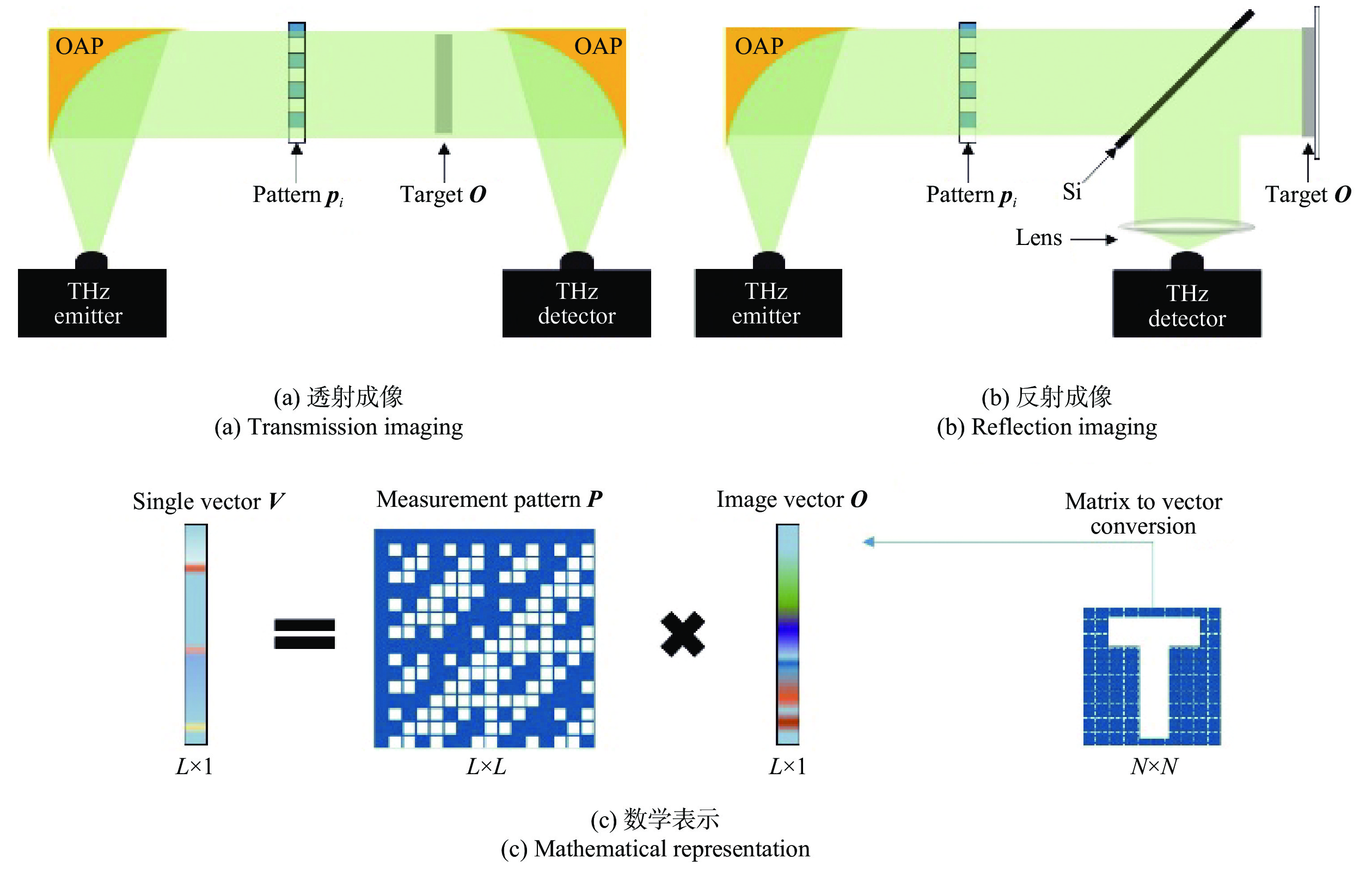
Fig. 1. Light path design of transmission(a) and reflection(b) and mathematical description (c) of terahertz single-pixel imaging based on modulator
![Schematic of the experimental setup for terahertz time-domain spectroscopy system[46]. (a) The different colors correspond to different delay-line positions, these positions correspond to different time points in Fig.(b); (b) Measured THz time-domain signal; (c) The amplitude and phase of a signal in the frequency domain](/richHtml/irla/2021/50/12/20210717/img_2.jpg)
Fig. 2. Schematic of the experimental setup for terahertz time-domain spectroscopy system[46]. (a) The different colors correspond to different delay-line positions, these positions correspond to different time points in Fig.(b); (b) Measured THz time-domain signal; (c) The amplitude and phase of a signal in the frequency domain
Fig. 3. Terahertz single-pixel computational imaging based on metal pattern modulator. (a) PCB modulator[50]; (b) Spinning metal disk modulator[51]
Fig. 4. Schematic diagram of terahertz single-pixel imaging structure based on metasurface modulator[56]. (a) Spatial distributon of maximum differential absorption for Hadamard pattern; (b) Image reconstruction using 64 masks with each mask displayed for 22.4 ms, giving a total image acquisition time of 1.43 s; (c) Photograph of the object studied. (d) Consecutive tiles show reconstruction using 45 Hadamard masks
Fig. 5. (a) Schematic of terahertz single-pixel imaging system based on the passivated silicon wafer[63]; (b) Comparison of reconstruction results between conventional high-resistive silicon and passivated silicon
Fig. 6. (a) Terahertz single-pixel imaging system and its imaging results based on nonlinear electro-optic crystals[70]; (b) Terahertz single-pixel imaging system and its imaging results based on spintronic materials[72]
Fig. 7. Fourier single-pixel computational imaging for the terahertz regime [81]. (a)-(d) Fourier spectrums at different sampling rates; (e)-(h) Inverse Fourier transform terahertz image
Fig. 8. (a) Network architecture of deep convolutional auto-encoder[86]; (b) Design of part of optimized patterns; (c) Experimental structure and video of single-pixel imaging
Fig. 9. (a) DCAN architecture [87]; (b) Qualitative and quantitative evaluation of conventional FSI and based on deep learning FSI
Fig. 10. Principle schematic of terahertz single-pixel computational imaging system at standoff distances and far-field imaging results[92]
Fig. 11. Schematic of terahertz single-pixel computational imaging construction and image reconstructed results [94-95]. The imaging resolution is 154 μm, 100 μm and 9 μm when the intrinsic silicon thickness is (a) 400 μm, (b) 110 μm and (c) 6 μm, respectively
Fig. 12. Structural schematic of time-resolved nonlinear ghost imaging and hyperspectral reconstructed results[97]
Fig. 13. (a) Terahertz recognition experimental setup of target; (b) Perfor- mance evaluation (confusion matrices) of the object recognition method[100]
| |||||||||||||||||||||||||||||||||||||||||||||||||||||||||||||||||||||||
Table 1. Summary of terahertz wave mask technology
|
Table 2. Comparison of technical indexes of single-pixel imaging algorithms


Set citation alerts for the article
Please enter your email address

© Copyright 2018-2021 | Chinese Laser Press. All Rights Reserved 沪ICP备15018463号-20