Shiyu Zhang, Quanjun Pan, Xu Fang, Kening Mao, Hui Ye. Fabrication and characteristics of silicon-rich oxide thin films with controllable compositions[J]. Chinese Optics Letters, 2016, 14(5): 051603
Copy Citation Text
Silicon-rich oxide films with controllable optical constants and properties are deposited by the reactive magnetron sputtering method on a Si target. The O/Si atomic ratio of is tuned from 0.12 to 1.84 by adjusting the oxygen flow rate, which is found to be a more effective way to obtain films compared with changing the oxygen content [ ratio]. The optical properties of films can be tuned from semiconductor to dielectric as a function of ratio . The structures and components are also investigated by an x ray photoelectron spectroscopy analysis of the Si 2p core levels, the results of which exhibit that the structures of can be thoroughly described by the random bonding model.
During the last decade, silicon-based nanostructured materials have gained much attention owing to their fundamental properties and optoelectronic applications[1–4]. Among them, silicon-rich oxide (SRO) films have been intensely investigated because of their unique characteristics and wide uses in various situations, such as insulating dielectric films in multilevel interconnects, detector and sensor applications, and in solar energy devices[5,6]. While in other optoelectronic devices, these materials also play an important role since the photoluminescence (PL) wavelength can be tuned by varying the oxygen content of ()[1,7,8]. Moreover, SRO films have recently been employed as a material to fabricate Si nanocrystals by annealing, which is also a candidate for active light sources (light emitters)[9–12]. SRO films can also be applied to anti-reflection or highly reflective optical coatings, for their refractive index varies with stoichiometry in a wide range[13–16]. Therefore, it is of great importance to characterize the material as a function of compositions and deposition conditions.
The methods employed to fabricate SRO films are various and include ion beam sputtering[17], chemical vapor deposition (CVD)[18–20], and magnetron sputtering from compound targets or reactive sputtering from a Si target[21,22]. For optoelectronic devices or other applications, low temperature deposition of the films was preferred, as well as the precise control of the composition and the thickness of the films. Under such circumstances, magnetron sputtering is more desirable. Previously, the influence of the oxygen flow rate (OFR) on the structural and optical properties of SRO films prepared by CVD was investigated by Song et al.[18,19]. Iwamori et al.[23] reported the effect of oxygen partial pressure on SRO films deposited by sputtering. However, they all studied on only one parameter (OFR or oxygen content) in the reaction procedure because these two parameters were generally considered to be the same, and few studies on the influence of both parameters during RF reactive magnetron sputtering have been reported. Actually, OFR and oxygen content have different impacts on the sputtering process and they should be taken as two different parameters in order to control the composition of the films more precisely during reactive magnetron sputtering.
In this Letter, we focused our investigation on SRO thin films prepared by reactive magnetron sputtering with an Si target in an atmosphere. The influence of sputtering conditions on the microstructure, stoichiometry, refractive index, and other optical properties of the films were studied in detail. Particularly, the absolute OFR and the relative oxygen content [ ratio], as the two control parameters in the reactive sputtering process, were evaluated and compared. Finally, it was found that OFR played a more significant role in the sputtering process, and the relationships between the properties and the stoichiometry of the deposited films were presented.
Sign up for Chinese Optics Letters TOC. Get the latest issue of Chinese Optics Letters delivered right to you!Sign up now
The SRO samples were prepared on p-type Si wafer substrates and BK7 glass substrates using a Si target (3 inches in diameter, 99.99% purity), the source power of which was kept at RF 500 W. Prior to sputtering, the chamber was evacuated to less than . The working gas was a mixture of and Ar with different flow rates, while the total pressure was fixed at 0.1 Pa. A pre-sputtering step was performed in order to clean the target. During deposition, the substrate temperature was held as room temperature without an external heating process. The film thicknesses of all deposited samples were monitored by a crystal oscillator during the sputtering process. Although the oscillator reading was the same (100 nm) for all samples, the actual thickness was different because the compositions of the deposited films were changing according to the varied gas compositions. The value of the actual film thickness was kept in a range from 58 to 80 nm, and the measuring method will be discussed later. Table 1 presents the detailed process parameters used in this study for the reactive sputtering.
As shown above, two sets of sputtering parameters were applied. For #A samples, Ar flow rate was kept at 20 sccm and the flow rate was adjusted from 0 to 4 sccm, while for #B samples, the flow rate was constant. The effect of two different ways for controlling the ratio was then studied.
The chemical state, structure, and composition of all samples were determined through x ray photoelectron spectroscopy (XPS) measurements using an ESCALAB 250Xi x ray photoelectron spectroscope. The transmittance and reflectance spectra of the films were measured by a Shimadzu UV-3101 spectrophotometer in the range of 250–1800 nm. The refractive indices and extinction coefficients were calculated by the photometry method (by OptiLayer software), which involves choosing the appropriate dispersion models to fit the measured transmittance and reflectance curves. The film thickness was also determined by this method to estimate the deposition rate.
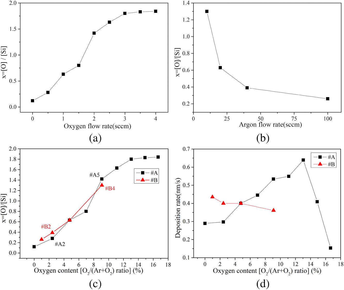
The chemical compositions of the films deposited on Si substrates at different ambiences was obtained from the XPS measurements. The atomic content of Si and O can be calculated from the peak area of O 1s and Si 2p, from which we can describe the stoichiometry of the films by the O/Si atomic ratio of . Figure 1(a) illustrates the variation of the ratio with the OFR of the #A samples. The ratio increased rapidly within the range of the small values of the OFR (0–2 sccm) and gently for OFRs larger than 2 sccm, indicating that the film stoichiometry was improved with the addition of in the ambience. For #B samples, the relationship between ratio and the Ar flow rate is presented in Fig. 1(b). It is reasonable that Ar affected the ratio in an opposite way compared to .
Figure 1.(a) O/Si atomic ratio of #A samples obtained from the XPS measurements as a function of the OFR. (b) The ratio of #B samples as a function of the argon flow rate. (c) The ratio and (d) the deposition rate of #A and #B samples as a function of the oxygen content [ ratio].
Figure 1(c) exhibits the ratio of all #A and #B samples as a function of the oxygen content in the sputtering ambient [ ratio]. The working pressure was kept at 0.1 Pa for both sets of samples so the samples who owned the same oxygen content would also share the same oxygen partial pressure.
As seen in Fig. 1(c), the trends of the two sets of samples are similar. Their O/Si atomic ratio both increased with the growing oxygen content. However, there is still a difference between #A and #B samples when we focus on two pairs of samples that had the same oxygen content but different OFRs; this information is presented in Table 2.
Table 2 shows the detailed parameters of the two pairs of samples. Although sample #A2 and sample #B2 had the same oxygen content, there was still a divergence between their O/Si atomic ratios . The one who had a greater OFR was found to be oxidized more easily and to achieve a higher value of . For another pair of samples, the OFR of sample #A5 was 2.0 sccm, larger than that of sample #B4. Same as above, sample #A5 had a higher value of ratio compared to sample #B4. Therefore, the OFR and oxygen content should be considered as two different parameters in the reactive sputtering procedure. These two parameters both would affect the reaction process while the OFR was in a more significant position. During the reactive sputtering procedure, the whole reactive magnetron sputtering should be considered as a transient process rather than a steady-state process because most injected oxygen in the chamber was consumed by pure Si or Si suboxide. In this case, the absolute amount of inlet oxygen is the key point. Although the oxygen content did have an impact on the reaction process, as a low oxygen content would lead to low molecule collision probabilities, a higher OFR means more amount of inlet oxygen during the process, thus resulting in more oxidized films. Therefore, the OFR should be paid more attention during the reactive sputtering procedure, in addition to the oxygen content and ratio.
In addition, the discrepancy between the effect of absolute OFR and of the relative oxygen content on the films was also confirmed by the deposition rates of the two sets of samples in Fig. 1(d). As we can see from the black square dots that represent the #A samples, the deposition rate varied with the oxygen content. When the oxygen content increased from 0% to about 12%, deposition rate climbed from 0.29 to 0.64 nm/s. As the oxygen content continued to increase, the deposition rate dropped dramatically down to 0.15 nm/s. The various changes of the deposition rate depended on the state of the Si target in the reactive sputtering, where two opposite processes existed on the target surface, i.e., sputtering and film formation due to oxidation. Initially, the deposition increase along with the oxygen content rate could be attributed to the relatively low oxygen content. In this case, the most oxidation occurred on the substrate and the target surface was almost Si, presenting a semiconductor state. Once a certain oxygen content had been reached, the deposition rate declined rapidly, which could be explained by the fact that the surface of Si target was oxidized. The oxidation layer was thickening, for its formation was faster than the sputtering, thus leading to a further decrease of the deposition rate[15,17]. For the #B samples, as a comparison, it was obviously that deposition rate changed little with the oxygen content, as the absolute OFR of the #B samples was kept at 1 sccm. Therefore, the deposition rate was more sensitive to the OFR than the oxygen content; in other words, the primary affecting factor in the reactive sputtering process was the OFR instead of the oxygen content. Furthermore, the O/Si atomic ratio of films along with their properties can be continuously adjusted by controlling the ambience precisely. The properties of films changing with the O/Si atomic ratio was also investigated.
To discuss the properties of films with various ratios , the #A samples were deposited on BK7 glass substrates whose ranges from 0.11 to 1.84. In the wavelength region of 250–1800 nm, pure silicon shows significant absorption, while pure has a high transmittance. As an intermediate state between Si and , the films presented a gradual transitional behavior from Si to in the transmittance spectrum. Figure 2(a) demonstrates the variation of the transmittance spectrum with O/Si atomic ratio for the films deposited on glass substrates. With the decreasing Si atom content, the transmittance of the samples was improved steadily. When the ratio was larger than 1.42, the transmittance presented smooth changes and tend to be saturated as reached 1.83. The changes in the transmittance of the films partly reflected the changes in their structures and components.
Figure 2.(a) Transmittance and (b) the refractive indices of films (#A samples) with various O/Si atomic ratios x values. (c) The refractive index and the extinction coefficient of films (#A samples) as a function of ratio at 550 nm wavelength.
In addition, the refractive indices of the films at different wavelengths deduced from the transmittance and reflectance spectra exhibited the same tendency, as shown in Fig. 2(b). The refractive index lines moved down with the increasing O/Si atomic ratio . Particularly, Fig. 2(c) presents the refractive index () and extinction coefficient () of the deposited films at the 550 nm wavelength. It can be seen that the optical constants were closely linked with the O/Si atomic ratio . The refractive index was 3.17 at a 0.12 ratio and dropped to a 1.48 when ratio reached 1.80. A further increase of would not have a great impact on the refractive index, as the silicon in the films was nearly fully oxidized and the refractive index was very close to that of ()[24]. On the other hand, the extinction coefficient reduced from 0.25 to almost 0 as ratio grew from 0.12 to 0.84, indicating a cease in the film absorption. When ratio started to increase from 1.42, the extinction coefficient would not change as rapidly as the refractive index. The behaviors of the film transmittance, refractive index, and extinction coefficient under various ratios could be explained by the changes of the structures and components. When ratio was at a low value, the films were similar to pure Si ()[25], presenting lower transmittance and a larger refractive index. Along with the raising value of , the films become more oxidized and their structures and components were much closer to . Consequently, the films with various refractive indices within a wide range can be obtained by tuning the O/Si atomic ratio .
For further discussion on the changes of the structures and the components of the deposited films during the oxidation, two models[1,20,26,27] are proposed to describe an network. One is the random bonding model (RBM), in which a structure was characterized by a statistical contribution of five different local bonding units, Si─(), , 1, 2, 3, 4. The other one is the random mixture model (RMM), which describes the structure as a mixture of Si─Si and Si─O bonding, i.e., Si and clusters were randomly arranged (or oriented) in the region. XPS measurements were applied to analyze the structures and components of the deposited films. Figure 3 illustrates the XPS spectra (Si 2p core level) for the deposited films with the labels #A1, #A3, #A4, #A5, and #A9, corresponding to the O/Si atomic ratios of 0.12, 0.63, 0.80, 1.42, and 1.84, respectively. Apparently, the Si 2p core peaks move from Si to with the increasing OFR, presenting the transition from the semiconductor Si state to the dielectric state. Moreover, it was obvious that there were Si suboxides (, and ) in our case, which is consistent with the prediction by the RBM model hypothesis rather than RMM model, in which case there should be just two peaks (Si and ). The deconvolution procedure is similar to the approach in Ref. [28]. First, the deconvolution of the peak from sample #A1 was conducted by decomposing the line into two Gaussians with the intensity ratio and a fixed spin-orbit splitting of 0.6 eV as an atomic property. Sample #A9 was fitted by a single Gaussian with the position of 103.7 eV corresponding to the line. The other samples were decomposed into , , , , and peaks by keeping a constant energy shift of , , and peaks from the midpoint between the two spin-orbit splitting components of peak to peak. Then the peaks of , and were obtained at the positions around 100.5, 101.6, and 102.6 eV, and the peak values were in agreement with Miyazaki et al.[29,30]. According to the RBM model, was homogeneous in the atomic distribution; thus, the intensities of different Si ionization states can be calculated by the following equation[27]: where is the oxidation state of silicon, namely 0, 1, 2, 3, and 4. In the RMM model, a simple mixture of only Si and is assumed, and the intensities are
Obviously, the intensities of different Si ionization states obtained from the fit agree better with the RBM model than with the RMM model. In the right part of Fig. 3, the calculated data according to the Eq. (1) (RBM model) and the XPS experimental data were compared. They agree well for sample #A1, while for the other samples, they do not match quite as well but the overall trends are the same.
Figure 3.XPS spectra of sample #A1, #A3, #A4, #A5, and #A9, corresponding to the O/Si atomic ratios of 0.12, 0.63, 0.80, 1.42, and 1.84, respectively. On the left side, the red hollow circles represent the experimental data and the black solid lines are the fitted components (, , , , and peaks) of the Si 2p core level and the sum line of the peaks. On the right side, the red dots represent the relative intensities of the components in the Si 2p core level and the black squares are the components calculated according to the RBM model.
Thin films are deposited under a mixture of oxygen and argon ambience using the reactive magnetron sputtering method. By changing the flow rate of oxygen and argon, the properties of the films are continuously modulated over a wide range. During the adjustment of the process parameters, the OFR is found to be more significant compared to the oxygen gas concentration [ ratio], as the O/Si atomic ratio is tuned from 0.12 to 1.84 when the OFR increases from 0 to 4 sccm at a constant Ar flow. A relationship between ratio and the optical properties of films is also presented and the refractive indices vary from 1.48 to 3.17 accordingly. Furthermore, the XPS spectra of the Si 2p core levels clearly show the phase separation of films with the increasing ratio ; the structure can be fully described by the RBM model. The above discoveries that the properties and structures of films can be continuously and effectively adjusted from semiconductor to dielectric by varying the OFR can give a better reference for subsequent studies.
[28] D. Ristić, M. Ivanda, G. Speranza, Z. Siketić, I. Bogdanović-Radović, M. Marciuš, M. Ristić, O. Gamulin, S. Musić, K. Furić, G. C. Righini, M. Ferrari. J. Phys. Chem. C, 116, 10039(2012).
Shiyu Zhang, Quanjun Pan, Xu Fang, Kening Mao, Hui Ye. Fabrication and characteristics of silicon-rich oxide thin films with controllable compositions[J]. Chinese Optics Letters, 2016, 14(5): 051603