
Zilan Deng, Fengjun Li, Tan Shi, Guoping Wang. Metagratings for Controlling Diffractive Optical Fields: Physics and Applications[J]. Acta Optica Sinica, 2021, 41(8): 0823011
- Acta Optica Sinica
- Vol. 41, Issue 8, 0823011 (2021)
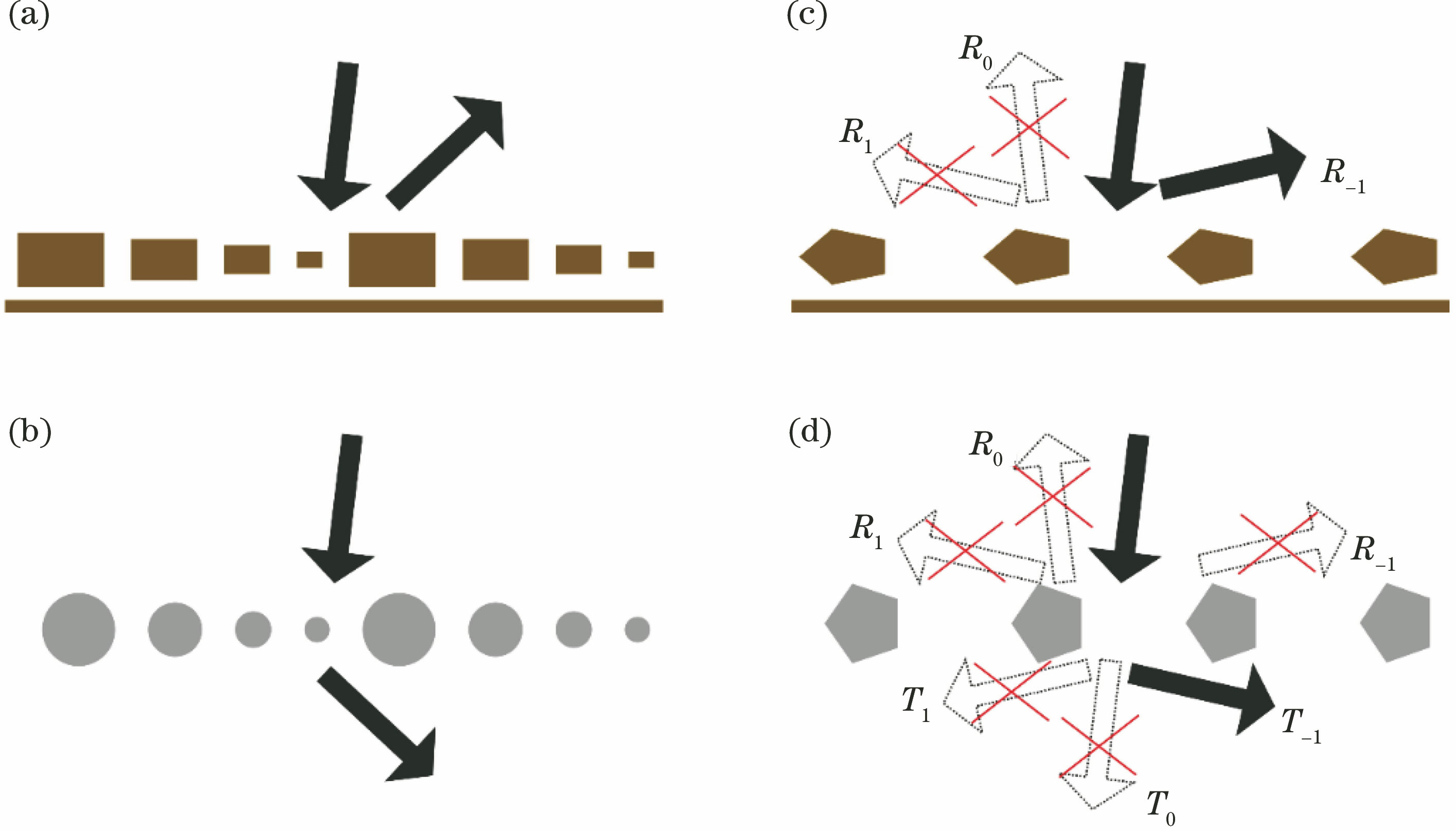
Fig. 1. Schematic for comparison between phase-gradient metasurfaces and single unit-cell metagrating structures. (a) Reflection and (b) transmission phase-gradient metasurfaces; (c) reflection and (d) transmission single unit-cell metagrating surfaces
![Symmetric reflection metagrating[29]. (a) Schematic of metallic groove metagrating; (b) k-space diffraction order chart composed of multiple Wood anomaly lines;(c) R-12 versus incident angle and wave number; (d) -1th and 0th order diffraction efficiency spectra and local mode amplitude spectra; (e) magnetic field (Hy) distribution diagram for perfect retro-reflection with incident angle of 30°](/richHtml/gxxb/2021/41/8/0823011/img_2.jpg)
Fig. 2. Symmetric reflection metagrating[29]. (a) Schematic of metallic groove metagrating; (b) k-space diffraction order chart composed of multiple Wood anomaly lines;(c)
Fig. 3. Asymmetric reflection metagrating[28]. (a) Metagrating composed of bianisotropic unit cells array with perpendicular electric resonance and magnetic resonance as well as schematic of asymmetric perfect diffraction; (b) parameter scanning image of cancellation factor under normal incidence; (c) diffraction efficiency of each diffraction order corresponding to normalized frequency denoted by red star in Fig.3 (b); (d) distributions of incident and reflected fields at designed frequency
Fig. 4. Symmetric transmission metagrating. (a) Principle diagram of plane wave diffraction from all-dielectric metagrating[69];(b) normalized scattering spectra of electromagnetic multipoles excited by p-polarized wave and s-polarized wave, respectively[69];(c) experimental demonstration of realization of beam bending with all-dielectric metagrating[71]; (d) schematic of transmission SiNx metagrating[72];(e) theoretical efficiency diagram of perfect transmission end diffraction[72]; (f) -1th order diffraction efficiency diagram for large angle and wide bandwidth[72]; (g) magnetic field pattern of perfect transmission end diffraction[72]
Fig. 5. Asymmetric transmission metagrating. (a) (Left) dielectric double-ridge waveguide with different widths and free-space radiation under certain phase difference and (right) far-field response image of double-ridge metagrating[64]; (b) extraordinary diffraction of bianisotropic transimission metagrating[61]; (c) transmission metagrating with fish-shaped structure[65]; (d) broadband large-angle asymmetric diffraction kissing double-nanopillar metagrating[74]; (e) freeform metagrating constructed using topological optimization[66]; (f) metagrating constructed by deep learning[77]
Fig. 6. Reconfigurable metagrating. (a) Schematic of reconfigurable metagrating composed of metal-graphene-metal sandwiched structure[79]; (b) schematic of spin-locked reflection of right-handed circularly polarized beam under varying incident angles with reconfigurable spin-locked reflection metagrating[82]
Fig. 7. Applications of metagrating lenses with large numerical aperture. (a) (Upper)SEM images of metagrating lens are displayed (scale bars indicating 10 μm, 5 μm, and 500 nm from left to right), (middle) focal field distributions of metalens in xz plane and xy plane, and (down) normalized intensity map along z direction at x=0 and normalized intensity map along x direction at z=45.05 μm[83]; (b) (upper) design diagram of hybrid metalens and actual metalens (bottom left) phase distribution and structure diagram of phase-gradient metasurface, (bottom right) structure diagram of wide angle deflection metagrating, diffraction efficiencies of metagrating (dot) and diffraction efficiencies of phase-gradient metasurface (solid line) under different diffraction angles[84]
Fig. 8. Achromatic focusing of metagrating[85]. (a) Schematics of beam deflection of coaxial small-angle achromatic metasurface and off-axis wide-angle achromatic metasurface; (b) structural diagrams of off-axis wide-angle achromatic metal groove metagrating; (c) effect diagrams of achromatic focusing
Fig. 9. Multifunctional device with angle selectivity of metagrating[86]. (a) Flow chart of extraordinary optical transmission (EOT), total internal reflection (TIR) and extraordinary optical diffraction (EOD) of multifunctional metasurface; (b) phase profiles of EOT, TIR and EOD at different incident angles and incident wavelengths; (c) numerical simulation results of EOT, TIR and EOD focusing at different incident angles
Fig. 10. Applications of metagrating holograms with ultra-large angle tolerance. (a) Metasurface hologram device designed by sub-wavelength dielectric metagratings and detour phase[32]; (b) metasurface hologram device with large angle tolerance designed by subwavelength metal metagratings[46]; (c) metasurface hologram device based on perfect diffraction dielectric metagratings[72]
Fig. 11. Metagratings used for converting surface plasma polariton (SPP) into arbitrary free-space wavefront. (a) Schematic of conversion from SPP wave to free-space wave through diffraction orders of metagrating[88]; (b) modulated metagrating for free-space Airy beam generation by SPP excitation[88]; (c) modulated metal metagrating used for 3D plasmonic micro-projector[89];(d) modulated metallic slit metagrating used for conversion from SPP waves with different polarization and propagation directions to different free-space holographic images[90]

Set citation alerts for the article
Please enter your email address
© Copyright 2018-2021 | Chinese Laser Press. All Rights Reserved 沪ICP备15018463号-20