• Photonics Research
  • Vol. 10, Issue 5, 1271 (2022)
Zhuohui Yang1, Zhengqing Ding1, Lin Liu1, Hancheng Zhong1, Sheng Cao1, Xinzhong Zhang1, Shizhe Lin1, Xiaoying Huang1, Huadi Deng1, Ying Yu1、*, and Siyuan Yu1、2
Author Affiliations
  • 1State Key Laboratory of Optoelectronic Materials and Technologies, School of Electronics and Information Technology, Sun Yat-sen University, Guangzhou 510275, China
  • 2e-mail: yusy@mail.sysu.edu.cn
  • show less
    DOI: 10.1364/PRJ.454200 Cite this Article Set citation alerts
    Zhuohui Yang, Zhengqing Ding, Lin Liu, Hancheng Zhong, Sheng Cao, Xinzhong Zhang, Shizhe Lin, Xiaoying Huang, Huadi Deng, Ying Yu, Siyuan Yu. High-performance distributed feedback quantum dot lasers with laterally coupled dielectric gratings[J]. Photonics Research, 2022, 10(5): 1271 Copy Citation Text show less
    Material properties of InAs/GaAs QD lasers. (a) Cross-sectional scanning electron microscope (SEM) image of layer stack of the epi-wafer. The inset is the transmission electron microscope (TEM) image of the five QD layers. (b) Photoluminescence spectrum of the QD active layers on GaAs. The inset shows the atomic force microscope (AFM) image of an uncapped QD layer. (c) Light–current–voltage (L–I–V) characteristics of the fabricated laser with a length of 2000 μm and its temperature dependence under continuous-wave (CW) condition ranging from 25°C to 115°C. The inset shows the natural logarithm of threshold current versus stage temperature. The dashed line represents linear fitting to the experimental data.
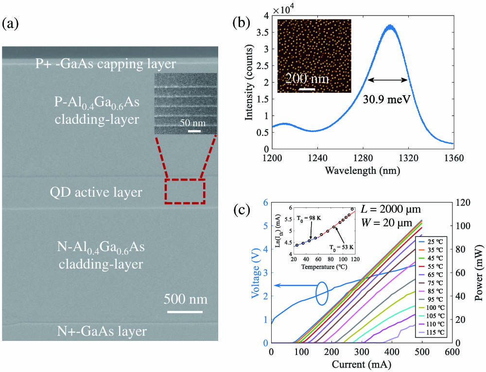
    Fig. 1. Material properties of InAs/GaAs QD lasers. (a) Cross-sectional scanning electron microscope (SEM) image of layer stack of the epi-wafer. The inset is the transmission electron microscope (TEM) image of the five QD layers. (b) Photoluminescence spectrum of the QD active layers on GaAs. The inset shows the atomic force microscope (AFM) image of an uncapped QD layer. (c) Light–current–voltage (LIV) characteristics of the fabricated laser with a length of 2000 μm and its temperature dependence under continuous-wave (CW) condition ranging from 25°C to 115°C. The inset shows the natural logarithm of threshold current versus stage temperature. The dashed line represents linear fitting to the experimental data.
    (a) Schematic of the DFB laser structure, including the near-zero “footing” trapezoid waveguide and the α-Si gratings (not to scale); (b) cross-sectional SEM image of the trapezoid waveguide with θ=76°, with the α-Si and the ARP6200 photoresist layers also present; (c) SEM images of the etched α-Si gratings with a λ/4 phase shift in the middle; (d) microscope image of laser array.
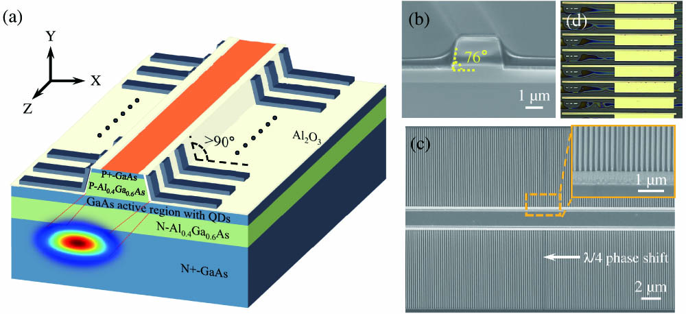
    Fig. 2. (a) Schematic of the DFB laser structure, including the near-zero “footing” trapezoid waveguide and the α-Si gratings (not to scale); (b) cross-sectional SEM image of the trapezoid waveguide with θ=76°, with the α-Si and the ARP6200 photoresist layers also present; (c) SEM images of the etched α-Si gratings with a λ/4 phase shift in the middle; (d) microscope image of laser array.
    (a) Typical L–I–V characteristics of a DFB laser with a 2.1 μm×1500 μm cavity at room temperature; (b) temperature-dependent L–I curves from the DFB laser, showing lasing up to 55°C under CW operation; (c), (d) optical spectra of the single DFB laser operating just below threshold (c) and at a drive current of 80 mA (d).
    Fig. 3. (a) Typical LIV characteristics of a DFB laser with a 2.1  μm×1500  μm cavity at room temperature; (b) temperature-dependent LI curves from the DFB laser, showing lasing up to 55°C under CW operation; (c), (d) optical spectra of the single DFB laser operating just below threshold (c) and at a drive current of 80 mA (d).
    (a) Wavelength shift with injection currents; (b) wavelength shift with heat-sink temperature; (c), (d) optical spectra and lasing frequencies of an LWDM DFB laser array measured at 100 mA.
    Fig. 4. (a) Wavelength shift with injection currents; (b) wavelength shift with heat-sink temperature; (c), (d) optical spectra and lasing frequencies of an LWDM DFB laser array measured at 100 mA.
    Measured RIN spectra at several bias currents at 25°C.
    Fig. 5. Measured RIN spectra at several bias currents at 25°C.
    (a) Experimental setup used for the long-delay feedback measurements. LF, lens fiber; PM, power meter; BOA, boost optical amplifier; OSA, optical spectrum analyzer; RIN, relative intensity noise; PC, polarization controller; ISO, optical isolator; BPF, bandpass filter. (b) Evolution of the SMSR with increasing feedback strength; the inset is the optical spectrum of the DFB laser as the feedback strength increases. (c) Change of RIN in the same DFB laser under 2.5×Ith, 3×Ith, and 4×Ith current injections. The inset is the frequency domain plot of RIN as a function of increasing feedback strength.
    Fig. 6. (a) Experimental setup used for the long-delay feedback measurements. LF, lens fiber; PM, power meter; BOA, boost optical amplifier; OSA, optical spectrum analyzer; RIN, relative intensity noise; PC, polarization controller; ISO, optical isolator; BPF, bandpass filter. (b) Evolution of the SMSR with increasing feedback strength; the inset is the optical spectrum of the DFB laser as the feedback strength increases. (c) Change of RIN in the same DFB laser under 2.5×Ith, 3×Ith, and 4×Ith current injections. The inset is the frequency domain plot of RIN as a function of increasing feedback strength.
    Coupling coefficient κ as a function of (a) grating duty cycle, (b) grating thickness, and (c) grating length.
    Fig. 7. Coupling coefficient κ as a function of (a) grating duty cycle, (b) grating thickness, and (c) grating length.
    YearSubstrateGratingκ  (mm1)Threshold Current (mA)Threshold Current Density (A/cm2)Power (mW)SMSR (dB)T(°C)RIN (dB/Hz)Anti-feedback (dB)Ref.
    2003GaAsGaAs sidewall39.350–14[48]
    2005GaAsMetal sidawall512>50[49]
    2011GaAsInGa/GaAs buried46.8104580[33]
    2011GaAsCr sidewall181500>105385–12[50]
    2014GaAsInGa/GaAs buried2.543.81830345860[51]
    2018GaAsGaAs sidewall3017102351[37]
    2018GaAsInGa/GaAs buried46.2110720>4070–150–8[52]
    2018Heterogenous integrated GaAs/SiSi7.79.52052.547100[53]
    2018Monolithic integrated GaAS/SiGaAs sidewall4.2125501.550[40]
    2020Monolithic integrated GaAs/SiAIGaAs/GaAs buried4.5204404.45070[34]
    2021Monolithic integrated GaAs/SiSi542502.86075[54]
    2021Heterogeneous GaAs/oxide/SiSi156.713476170–125[55]
    2021GaAsInGaP/GaAs buried1.69.3155055–150–6[24]
    2021GaAsAmorphous Si sidewall2.01857126.652.755–165–12.3This work
    Table 1. Comparison of the Performance of Our Device with Reference QD DFB Laser at 1310 nm
    Zhuohui Yang, Zhengqing Ding, Lin Liu, Hancheng Zhong, Sheng Cao, Xinzhong Zhang, Shizhe Lin, Xiaoying Huang, Huadi Deng, Ying Yu, Siyuan Yu. High-performance distributed feedback quantum dot lasers with laterally coupled dielectric gratings[J]. Photonics Research, 2022, 10(5): 1271
    Download Citation