• Chinese Journal of Lasers
  • Vol. 50, Issue 8, 0802403 (2023)
Yi Zhang*
Author Affiliations
  • Institute of Laser Engineering, Faculty of Materials and Manufacturing, Beijing University of Technology, Beijing 100124, China
  • show less
    DOI: 10.3788/CJL220840 Cite this Article Set citation alerts
    Yi Zhang. Laser Micro-Nano Patterning Based on Optical Dielectric Microsphere Array[J]. Chinese Journal of Lasers, 2023, 50(8): 0802403 Copy Citation Text show less
    COMSOL simulation results. (a) Diameter of microsphere is 5 µm; (b) diameter of microsphere is 1 µm
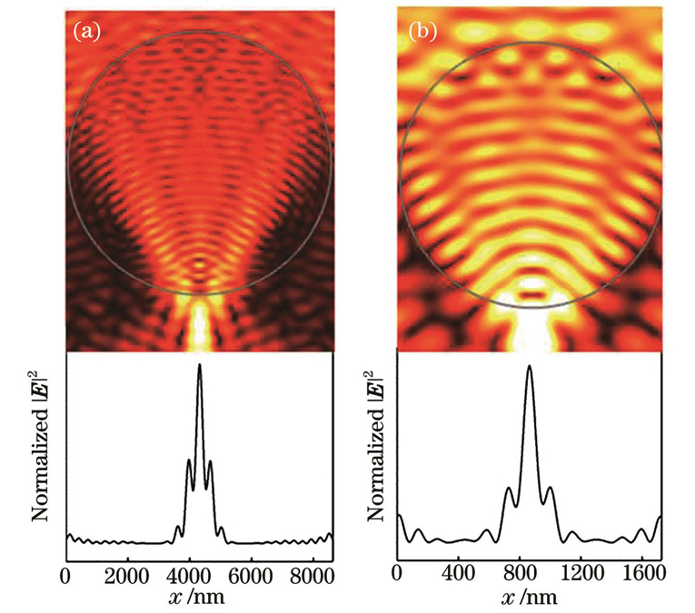
    Fig. 1. COMSOL simulation results. (a) Diameter of microsphere is 5 µm; (b) diameter of microsphere is 1 µm
    Effects of microsphere diameter and laser wavelength on machining accuracy
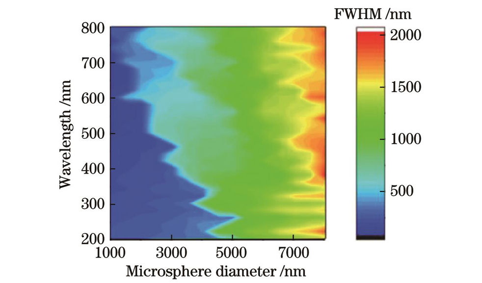
    Fig. 2. Effects of microsphere diameter and laser wavelength on machining accuracy
    Schematic diagram of experimental process
    Fig. 3. Schematic diagram of experimental process
    Silica microsphere monolayer dense array
    Fig. 4. Silica microsphere monolayer dense array
    Schematic diagram of laser light path
    Fig. 5. Schematic diagram of laser light path
    Effect of laser wavelength on gold film structure (25 nm gold film, 4.82 µm microspheres and 10 mJ/cm2 energy density). (a) 532 nm; (b) 355 nm; (c) 266 nm; (d) variation of hole diameter on gold film with energy density at different wavelengths
    Fig. 6. Effect of laser wavelength on gold film structure (25 nm gold film, 4.82 µm microspheres and 10 mJ/cm2 energy density). (a) 532 nm; (b) 355 nm; (c) 266 nm; (d) variation of hole diameter on gold film with energy density at different wavelengths
    Effect of microsphere diameter on gold film structure (532 nm laser, 25 nm gold film and 30 mJ/cm2 energy density). (a) 4.82 µm; (b) 2.53 µm; (c) 1.49 µm; (d) variation of hole diameter on gold film with energy density under different microsphere diameters
    Fig. 7. Effect of microsphere diameter on gold film structure (532 nm laser, 25 nm gold film and 30 mJ/cm2 energy density). (a) 4.82 µm; (b) 2.53 µm; (c) 1.49 µm; (d) variation of hole diameter on gold film with energy density under different microsphere diameters
    Effect of gold film thickness on gold film structure (532 nm laser, 4.82 µm microspheres and 20 mJ/cm2 energy density). (a) 10 nm; (b) 25 nm; (c) 40 nm; (d) variation of hole diameter on gold film with energy density under different gold film thicknesses
    Fig. 8. Effect of gold film thickness on gold film structure (532 nm laser, 4.82 µm microspheres and 20 mJ/cm2 energy density). (a) 10 nm; (b) 25 nm; (c) 40 nm; (d) variation of hole diameter on gold film with energy density under different gold film thicknesses
    Processed holes with diameter about 100 nm at optimal parameter (laser wavelength is 532 nm, gold film thickness is 25 nm, microsphere diameter is 1.49 μm and laser energy density is 25 mJ/cm2)
    Fig. 9. Processed holes with diameter about 100 nm at optimal parameter (laser wavelength is 532 nm, gold film thickness is 25 nm, microsphere diameter is 1.49 μm and laser energy density is 25 mJ/cm2)
    Effect of step on line processing. (a) Only one point is machined; (b) machining step is 400 nm; (c) machining step is 800 nm; (d) machining step is 1200 nm
    Fig. 10. Effect of step on line processing. (a) Only one point is machined; (b) machining step is 400 nm; (c) machining step is 800 nm; (d) machining step is 1200 nm
    Effect of energy density on line processing. (a) Energy density is 25 mJ/cm2; (b) energy density is 23 mJ/cm2; (c) energy density is 20 mJ/cm2
    Fig. 11. Effect of energy density on line processing. (a) Energy density is 25 mJ/cm2; (b) energy density is 23 mJ/cm2; (c) energy density is 20 mJ/cm2
    Processed patterns. (a) Processed pattern Ton 4.82 µm microsphere; (b) processed patternCon 4.82 µm microsphere; (c) processed patternOon 2.53 µm microsphere
    Fig. 12.

    Processed patterns. (a) Processed pattern T on 4.82 µm microsphere; (b) processed pattern C on 4.82 µm microsphere; (c) processed pattern O on 2.53 µm microsphere

    No.Wavelength /nmDiameter of dielectric microspheres /µmThickness of goldfilm /nmCritical energy density ofpore-out /(mJ·cm-2Gold film holediameter /nm
    12664.821041200
    23554.821081000
    35324.8210201600
    42664.822561000
    53554.82258500
    65324.822525300
    72664.82408800
    83554.824015600
    95324.8240401300
    102662.53104800
    113552.53106800
    125322.531020600
    132662.53256500
    143552.53258400
    155322.532525200
    162662.534081000
    173552.5340151300
    185322.5340401300
    192661.49104500
    203551.49106400
    215321.491020200
    222661.49256200
    233551.49258150
    245321.492525100
    252661.494010300
    263551.494025250
    275321.494045400
    Table 1. Critical energy density of pore-out under different process parameters and hole diameter of gold film processed under the energy density
    Yi Zhang. Laser Micro-Nano Patterning Based on Optical Dielectric Microsphere Array[J]. Chinese Journal of Lasers, 2023, 50(8): 0802403
    Download Citation