Laser is a tool widely used in industrial manufacturing that has the advantage of non-contact technology. Lasers can be used to produce complex structures without photomasks in air, vacuum, or water. In addition, lasers can be easily focused down to the micrometer scale; therefore, they can be used in microdevice fabrication. In particular, they are widely used in marking, drilling, annealing, surface modification, and other processes in the microelectronics industry. However, because of the diffraction limit, the minimum achievable resolution of a laser is limited by its wavelength. The microsphere provides a mechanism to manipulate light in a way that cannot be achieved using traditional optical components. The focusing and scattering of light can be manipulated at the microscopic scale using microspheres. The limitation caused by the diffraction limit is overcome based on near-field optics. Therefore, optical dielectric microspheres are used to modulate the laser and realize micro-nano processing with a resolution above the diffraction limit. On this basis, researchers have also overcome the difficulties of traditional micro-nano processing techniques, such as slow processing and inability to achieve large-area one-time processing, through self-assembled microsphere array technology. At the same time, researchers have also realized the processing of arbitrary micro-nano patterns using off-axis laser irradiation technology. In this study, micro-nano processing was realized by modulating the laser with a densely packed single-layer dielectric microsphere array. Pattern processing, which breaks through the diffraction limit resolution, was realized on a gold film on the surface of the microsphere.
The near-field optical enhancement effect of the microspheres was simulated and analyzed, and the mechanism of the effect of laser direct writing technology on the gold micro-nano structure using the microsphere array was obtained. The experimental method (Fig. 3) includes the following steps: preparing the polydimethylsiloxane (PDMS) thin film, closely laying the dielectric microsphere array on the PDMS film (Fig. 4), ion sputtering the gold plating film, laser vertical irradiation for single-hole processing, laser changing angle irradiation for line processing (Fig. 5), and multi-point processing to realize patterning.
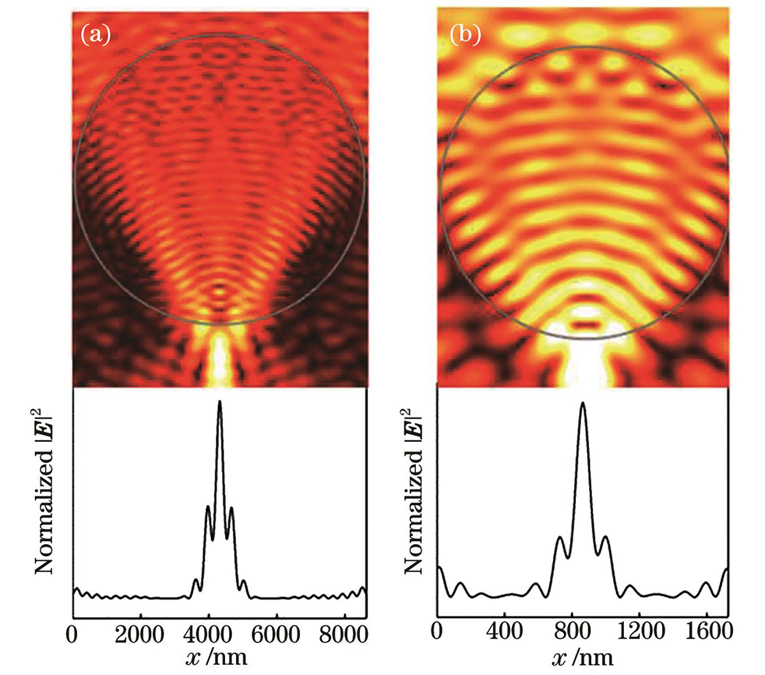
The optical field intensity of the microspheres was simulated (Fig. 1). The effects of the microsphere size and laser wavelength on the optical field enhancement and full width at half maximum (FWHM) of the laser peak were determined (Fig. 2). The micro-nano-processing technique of microspheres using a Mie scattering laser was studied. Process parameters such as laser wavelength (Fig. 6), size of microspheres (Fig. 7), thickness of ion sputtering coating (Fig. 8), laser off-axis irradiation offset angle (Fig. 10), and laser irradiation energy density (Fig. 11) were optimized. The morphological characteristics of the gold micro-nano structure were characterized by scanning electron microscopy, and the influence laws of each process on the processing results were summarized to optimize the process parameters. The experimental results show that 100 nm diameter holes can be machined under the following process parameters: laser wavelength of 532 nm, gold film thickness of 25 nm, microsphere size of 1.49 µm, and laser energy density of 25 mJ/cm2 (Fig. 9). Simple pattern processing was performed, and the line width of the processed pattern was close to 280 nm at half wavelength under the following process parameters: laser wavelength of 532 nm, gold-film thickness of 25 nm, microsphere size of 2.53 µm, laser energy density of 30 mJ/cm2, and processing line width of 1/3 for each step (Fig. 12).
This paper introduces a method for processing gold films on the surface of microspheres by modulating laser with a single-layer optical dielectric microsphere array. Using this method, the gold film on a large-area microsphere array can be processed at a high rate and resolution in the micron order. The optical near-field of the dielectric microsphere array was analyzed to realize the convergence of light beyond the diffraction limit. Along with the software simulation of the regulation of the light field by microspheres, the influences of the size of the microsphere and laser wavelength on the machining accuracy were discussed. Then, through experiments using different fabrication processes, the influences of the laser wavelength, size of the dielectric microspheres, thickness of the ion sputtering coating, and energy density of the laser irradiation on the processed gold micro-nano structures were studied and discussed. Finally, the optimal processing parameters were obtained, and a gold single-hole structure of approximately 100 nm was obtained. The step and line widths suitable for patterning were studied by changing the incident angle of the laser. Simple pattern processing was performed, and the linewidth of the processed pattern was close to 280 nm.