1Nanjing University, College of Engineering and Applied Sciences, National Laboratory of Solid State Microstructures, Key Laboratory of Intelligent Optical Sensing and Manipulation, Collaborative Innovation Center of Advanced Microstructures, Nanjing, China
2Jiangsu Industrial Technology Research Institute, Institute for Smart Liquid Crystals, Changshu, China
Overcoming chromatic aberrations is a vital concern in imaging systems in order to facilitate full-color and hyperspectral imaging. By contrast, large dispersion holds opportunities for spectroscopy and tomography. Combining both functions into a single component will significantly enhance its versatility. A strategy is proposed to delicately integrate two lenses with a static resonant phase and a switchable geometric phase separately. The former is a metasurface lens with a linear phase dispersion. The latter is composed of liquid crystals (LCs) with space-variant orientations with a phase profile that is frequency independent. By this means, a broadband achromatic focusing from 0.9 to 1.4 THz is revealed. When a saturated bias is applied on LCs, the geometric phase modulation vanishes, leaving only the resonant phase of the metalens. Correspondingly, the device changes from achromatic to dispersive. Furthermore, a metadeflector with tunable dispersion is demonstrated to verify the universality of the proposed method. Our work may pave a way toward active metaoptics, promoting various imaging applications.
The development of nanostructured metasurfaces has offered unprecedented capabilities for the advance of planar optics.1–3 Among various metadevices, the metalens attracts widespread attention due to practical applications in imaging and spectroscopy.4–7 Recently, metalenses composed of specific subwavelength metallic or dielectric resonator arrays have been developed for multifunctional wavefront manipulations,8–12 replacing the traditional refractive lenses made of precisely polished crystals or polymers. These metalenses embrace the trend of miniaturization and integration of photonic systems. Nevertheless, their functions remain static once they are fabricated. Therefore, many researchers are focusing on realizing active metalenses via introducing MEMS,13 semiconductors,14,15 phase-change materials,16–18 graphene,19 and liquid crystals (LCs)20,21 with external field induced responsivity. The majority of them possess either switchable bifocal properties or a limited tuning range. Until now, dynamic functions, especially continuously variable focal length or tunable chromatic aberration, have remained formidable challenges.
In many cases, metalenses suffer from large chromatic aberrations, which severely degrade the resolution of full-color and hyperspectral imaging. Compared with optical or near-IR metalenses, the chromatic aberration of their terahertz (THz) counterparts is more significant, due to the broadband of THz spectrum.22 It induces a frequency-varying focal length and drastically degrades the resolution of spectral-resolved THz imaging.23,24 To solve this problem, mechanical scanning along the optical path is required to capture images at different frequencies,25 which makes the detection and analysis complicated and time-consuming. More recently, inspired by achromatic metalens designs in the visible and near-IR range,26–30 broadband achromatic focusing has been realized in the THz regime via dispersive phase compensation from C-shape silicon micropillar arrays.31 By contrast, for spectrographic and tomographic applications,32,33 large chromatism is favored to separate focal spots of different frequencies spatially without crosstalk.34,35 If dynamic alternation between the achromatic and dispersive focusing properties can be achieved using a single metalens, it would greatly promote the practical applications of spectroscopy and imaging systems.
In this paper, we propose a transmission-type THz metalens with tunable chromatic aberration. The metalens integrates a dielectric metasurface with photopatterned LCs and exhibits a broadband achromatism. When a saturated voltage is applied on the transparent graphene electrodes, a dispersive focusing function is revealed. The performance of the metalens is characterized and consistent with numerical simulations. Further, THz imaging performed with this metalens also verifies its tunable functions. This approach may open an avenue for designing active metalenses in versatile applications.
Sign up for Advanced Photonics TOC. Get the latest issue of Advanced Photonics delivered right to you!Sign up now
2 Results
2.1 Principle and Design
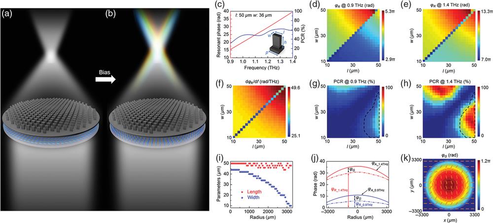
Figures 1(a) and 1(b) schematically illustrate the tunable functions of the proposed metalens. The achromatism is accomplished by delicately designing the integrated resonant phase () and geometric phase (). Geometries of silicon pillar meta-units36,37 vary from the center to the edge, enabling a frequency-dependent lens phase profile. The space-variant alignments of LCs38 perform a frequency-independent modulation. Without the applied voltage, it works as a broadband achromatic lens, where light within the designed spectrum deflects to the same focal spot. When applying a saturated bias on the graphene electrodes39 covered on both sides of the LC layer, LCs are reoriented perpendicularly to the substrates. Thus the modulation vanishes and only the of the metaunits works. Correspondingly, the device turns into a chromatic lens with an anomalous dispersion, i.e., the focal length decreases when the frequency increases.
Figure 1.Schematic function tunability and designs of the metalens. (a) The broadband achromatic focusing state without bias. (b) The dispersive focusing state with a saturated bias. The superstrate depicts the dielectric metasurface while the blue ellipsoids between the superstrate and substrate denote LCs. (c) Dependencies of (red curve) and PCR of a silicon pillar metaunit on . Inset shows the dimensions of the unit. Dependency of on and at (d) 0.9 and (e) 1.4 THz, respectively. (f) Dispersion ratio of the silicon pillar as a function of and under LCP incidence. Dependency of PCR on and at (g) 0.9 and (h) 1.4 THz. The region circled by the black dashed line indicates a PCR over 12% from 0.9 to 1.4 THz. (i) Designed and of the silicon pillars along from the center to the edge. (j) and at 0.9 (blue solid and dashed curves) and 1.4 THz (red solid and dashed curves) and residual . (k) Target and corresponding LC director distributions are labeled by the orange lines.
The generalized phase profile of an achromatic lens is expressed as where denotes the working frequency, is the light velocity in vacuum, is the focal length, and is the radius of an arbitrary point on the lens. The additional phase is only related to , which is introduced for dispersion compensation (see Fig. S1 in the Supplementary Material). If a linear function is established between and , namely, ( and are constants), can be transformed to
From Eq. (2), at a certain , the required shows a linear relationship with . Such a linear dispersion can be satisfied by high-order waveguide resonances excited inside the dielectric pillars with a high aspect ratio and large dielectric constant40 (Fig. S2 in the Supplementary Material). Apart from the former dispersion item achieved by the , the constant is frequency-independent and can be accomplished through introducing the , namely the Pancharatnam–Berry phase.41 It originates from the photonic spin–orbit interaction and can be created via controlling the geometric orientation angle of anisotropic media, e.g., LCs and metaresonators.42,43 Theoretically, is twice and conjugated at left-handed and right-handed circular polarization (LCP/RCP) incidences.
As a proof-of-concept demonstration, an achromatic lens with from 0.9 to 1.4 THz was designed. In Fig. 1(c), and the polarization conversion ratio (PCR, determining the efficiency of the metalens) of a silicon pillar metaunit with , , , and are simulated and presented as an example. To simplify the simulation, we fix and and then vary and in the range of 10 to to achieve a library of dispersion ratios (defined as ), as shown in Fig. 1(f). increases with and separately. The abnormal values along the diagonal are due to the near zero PCR when . and PCR are also related to and ; the dependencies of on them at 0.9 and 1.4 THz are shown in Figs. 1(d) and 1(e), respectively. The phase difference of on mirrored sides of is due to the additional induced by a 90-deg rotation of the metaunit. To achieve the desired achromatic property, the geometry of metaunits at different should be deliberately selected. In addition to the dispersion factor , should be further considered to maintain a lens profile. Figures 1(g) and 1(h) exhibit the dependency of PCR on and . For optimized efficiency, only parameters in the black-dashed region are used. Due to the limited range of ( at , to at , ), of the metalens is limited to , i.e., 54 units. According to this design, the and of the silicon pillars along are presented in Fig. 1(i). It is observed that remains nearly unchanged around , whereas gradually decreases from the center to the edge. Figure 1(j) plots the and at 0.9 and 1.4 THz. The -independent and -dependent gap between and can be compensated for by . The corresponding profile [Fig. 1(k)] can be precisely accomplished by locally varying the LC directors, as shown schematically in the overlay.
2.2 Focusing Performance Characterizations
Figures 2(a)–2(d) present the SEM images of the fabricated metasurface. Figure 2(a) shows a part of the metasurface from the top view. The silicon pillars close to the center and the edge are labeled by orange and blue dashed squares, respectively. Corresponding zoomed-in images in Figs. 2(b) and 2(c) show well-defined microstructures, which faithfully follow the design [Fig. 1(i)]. The cross-section image of the metasurface is exhibited in Fig. 2(d). Some broken pillars resulting from the damage caused in the cutting process are observed. Due to the different etching speeds for the varying aspect ratio in the fabrication, pillars near the edge [the right side in Fig. 2(d)] are higher than those near the center (left side) (detailed in Fig. S3 in the Supplementary Material). The photopatterned LCs are observed under the microscope with crossed polarizers. The optical image of the whole LC region is displayed in Fig. 2(e), in which the gray scales are consistent with the shown in Fig. 1(k). As the is pixelated with the same periodicity of as that of silicon metaunits, gray scale pixels are vividly revealed in the zoomed-in image in Fig. 2(f).
Figure 2.Characterization of the metalens. (a) SEM image of the metasurface (top view). Scale bar: . Zoomed-in images of the silicon pillars labeled by the (b) orange and (c) blue squares in (a), respectively. (d) Cross-section image of the metasurface. Scale bars in (b)–(d): . (e) Optical image of the LC layer under crossed polarizers. (f) A zoomed-in image labeled by the orange square in (e). Scale bars in (e) and (f) are 1 mm and , respectively.
We use a scanning near-field THz microscope (SNTM) to characterize the performance of the LC integrated metalens. The normalized intensity distributions from 0.9 to 1.4 THz with an interval of 0.1 THz are simulated and measured at the bias OFF and saturated states, respectively (Fig. S4 in the Supplementary Material). Figure 3(a) selectively reveals the simulated THz fields at 0.9, 1.1, and 1.4 THz in the plane at bias OFF. The measured remains unchanged around 12.0 mm within the designed spectrum [Fig. 3(b)], which is consistent with the simulation. Little distortions are observed at 0.9 and 1.1 THz, which is mainly attributed to the slightly tilt incidence of the THz beam. The THz fields in the plane () and the corresponding transverse intensity profiles are also exhibited, verifying the perfect achromatic focusing property. It is noticed that the is slightly smaller than the design as a result of the gradual etching depth deviation (see Sec. S2 in the Supplementary Material). This deviation is also considered in the simulation. After a square-wave alternating voltage (75 , 1 kHz) is applied, both the simulated and measured results [Figs. 3(c) and 3(d)] show a significant dispersion among different from 0.9 to 1.4 THz. It is noticed that, as the is spin-dependent, the metalens only works at the LCP THz incidence when the bias is OFF, whereas it works at both LCP/RCP incidences when the bias is saturated due to the spin-independent . LCs can be electrically tuned to match the half-wave conditions at different to generate a complete geometric phase modulation, contributing to the achromatic case. Mismatch from the half-wave condition causes the residual unmodulated wave, contributing to the dispersive case. Thus via tuning the applied voltage, the required circular polarization incidence of the metasurface is satisfied.
Figure 3.Focusing performance of the metalens. (a) Simulated THz fields in the plane and (b) measured THz fields in the and plane () at 0.9, 1.1, and 1.4 THz, respectively, when no bias is applied. (c) Simulated and (d) measured THz fields in the and plane () of the same sample with a saturated bias. Dashed lines in (a)–(d) label the corresponding focal planes. White curves in (b) and (d) depict the transverse intensity distributions at and 13.0 mm, respectively. (e) Simulated and measured , (f) FWHM at and 13.0 mm in (b) and (d), separately, and (g) measured device efficiency, as a function of . The black dashed line in (f) depicts the diffraction-limited FWHM.
The dependencies of on at both the bias OFF and saturated states are quantified in Fig. 3(e). The results satisfactorily verify the function tunability from achromatic to dispersive. Full-widths at half-maximum (FWHMs) of the intensity profile at different are shown in Fig. 3(f). The values at the achromatic state [ in Fig. 3(b)] are very close to the ideal diffraction limit ( NA), whereas distinct deviations are observed at the dispersive state [ in Fig. 3(d)] due to the defocusing at lower . Figure 3(g) exhibits the measured efficiency, which is defined as the ratio of THz intensity at the focal plane to the incident LCP THz power. The average efficiency of the dispersive case () is higher than that of the achromatic one (), which is attributed to the additional PCR loss caused by LCs. The total efficiency is determined by several factors: the PCR of the metaunits and LCs, the absorption and scattering of all transmitted layers, and the imperfect fabrication of the sample. These issues can be addressed by further optimizing the metaunit geometry and the LC layer thickness and introducing low-loss substrates (detailed analysis in Sec. S4 in the Supplementary Material).
2.3 Dynamic THz Imaging
The imaging performance of the metalens is further characterized, utilizing the setup schematically illustrated in Fig. 4(a). After generation with a photoconductive antenna,44 the linearly polarized THz wave is converted to LCP with a quarter-wave plate. The THz beam transmits the object and subsequently the metalens; then it is scanned by the probe. The object is a “smiling face” with a diffraction-limited resolution. The object distance and image distance are designed as both 24.0 mm to obtain an image with an equal size of the object when . The intensity and phase distributions from 0.9 to 1.4 THz with an interval of 0.1 THz are measured at the bias OFF and saturated states (Fig. S5 in the Supplementary Material). At the bias OFF state, a multispectral imaging is realized, where the smiling face can be distinctly observed at any within the spectrum. When the bias is saturated, the imaging quality becomes poorer at lower due to the deviation of from 12.0 mm. Figures 4(b)–4(e) show the corresponding intensity and phase distributions at 0.9 and 1.4 THz. The transverse intensities across two “eyes” and the “mouth” are clearly recognized in Figs. 4(b), 4(c), and 4(e), indicating a satisfactory imaging quality. The smiling face is distinguishable in corresponding phase distributions as well. However, the imaging effect is poor in Fig. 4(d) due to the remarkable defocusing. The imaging quality can be further enhanced via enlarging the NA of the metalens. A simple and effective method is increasing the of the silicon pillars while maintaining the other parameters (see Fig. S6 in the Supplementary Material).
Figure 4.Broadband THz imaging. (a) Schematic of the SNTM setup. The inset exhibits the micrograph of the object “smiling face,” where the scale bar indicates 1 mm. Measured intensity and phase distributions at (b) 0.9 and (c) 1.4 THz without bias. The white and orange curves depict the intensity profiles along the white and orange dashed lines, respectively. The outline of the object “smiling face” is labeled by black dashed lines in the phase diagrams. Measured intensity and phase distributions at (d) 0.9 and (e) 1.4 THz with a saturated bias.
The proposed strategy can be rationally extended to the design of various active metadevices beyond the metalens. We numerically demonstrate a beam deflector with tunable dispersion in Fig. S8. It is composed of silicon metaunits with geometries varying along the axis and LCs with gradient orientation distributions. The combination of and contributes to a fixed deflection angle of 17 deg from 0.9 to 1.4 THz. When the LCs are reoriented along the axis, the deflection becomes dispersive (details in Sec. S5 in the Supplementary Material).
3 Experimental Section
3.1 Sample Fabrication
The fabrication process of the LC integrated metalens is schematically illustrated in Fig. S9 in the Supplementary Material. The metasurface is fabricated via the standard photolithography process followed by a reactive ion etching on a -thick intrinsic silicon wafer. Then the residual photoresist is lifted off. Both the metasurface and silica substrate are ultrasonically cleaned and O-plasma treated for 10 min. Then they are transferred with few-layer graphene from copper foil (Six Carbon Technology, China). After that, they are spin-coated at 3000 rpm for 30 s with photoalignment agent SD145,46 (Dai-Nippon Ink and Chemicals, Japan) and baked at 100°C for 10 min to remove the solvent. Then the metasurface and silica substrate are assembled with a -thick Mylar spacer to form a cell. A digital micromirror device-based dynamic microlithography47,48 is employed to perform the photopatterning process. Then the LC NJU-LDn-449 with an average birefringence over 0.3 within the designed spectrum is infiltrated at 180°C and self-assembled to the desired orientations. The imaging object “smiling face” is fabricated via photolithography followed by an electron beam evaporation to deposit Au on the silicon substrate.
3.2 Numerical Simulation
The parameter sweep and selection of silicon pillar metaunits and the focusing performance simulation of the metalens are carried out using a commercial software (Lumerical FDTD Solutions). Due to the geometric symmetry of the lens, the model along the radius is established to simplify the simulation. The LC layer is divided into small domains. Each domain is set as a () cuboid. The LC is a diagonal dielectric material with (diagonal elements and ) and (diagonal element ). The LC director distributions are set by an LC orientation module. An LCP plane wave with a spectrum range from 0.9 to 1.4 THz is incident along the axis.
3.3 Characterizations
An SNTM setup (Terahertz Photonics Co., Ltd., China), which is based on the photoconductive THz generation and detection, is utilized to characterize the performance of the metalens. In the setup, a scanning tip fixed on a motorized stage [Fig. 4(a)] is utilized to record the field in the plane with a step size of 0.25 mm. The sample moves along the axis with a step size of 1 mm to capture the field in the plane. Then an interpolation algorithm is adopted to obtain the measured THz fields.
4 Conclusion
We developed an LC integrated metalens with tunable chromatic aberration. The geometric phase of photopatterned LCs and the resonant phase of the dielectric metasurface together contribute to the broadband achromatic focusing. While applying a saturated voltage to LCs, the geometric phase modulation vanishes and the metalens exhibits a dispersive focusing. Simulated and experimental results of such active functions reveal a good consistency. Moreover, multispectral THz imaging using this metalens is demonstrated, indicating great potential in advanced THz spectroscopy and imaging apparatuses. This strategy can also be extended to other electromagnetic spectra, e.g., the visible and near-IR, where lenses with integrated tunable functions are highly desired for full-color imaging and tomography. A metadeflector with tunable dispersion is further demonstrated, which verifies the versatility of the proposed solution for various metadevices toward active metaoptics.