• Photonics Research
  • Vol. 9, Issue 12, 2420 (2021)
Zhipeng Zhang, Manni Chen, Xinpeng Bai, Kai Wang, Huanjun Chen, Shaozhi Deng, and Jun Chen*
Author Affiliations
  • State Key Laboratory of Optoelectronic Materials and Technologies, Guangdong Province Key Laboratory of Display Material and Technology, School of Electronics and Information Technology, Sun Yat-sen University, Guangzhou 510275, China
  • show less
    DOI: 10.1364/PRJ.438204 Cite this Article Set citation alerts
    Zhipeng Zhang, Manni Chen, Xinpeng Bai, Kai Wang, Huanjun Chen, Shaozhi Deng, Jun Chen. Sensitive direct-conversion X-ray detectors formed by ZnO nanowire field emitters and β-Ga2O3 photoconductor targets with an electron bombardment induced photoconductivity mechanism[J]. Photonics Research, 2021, 9(12): 2420 Copy Citation Text show less
    Comparison of conceptual design of X-ray detectors and corresponding X-ray response mechanism. (a) Conventional X-ray detectors with TFT readout. (b) Proposed X-ray detectors with vacuum FEA readout.
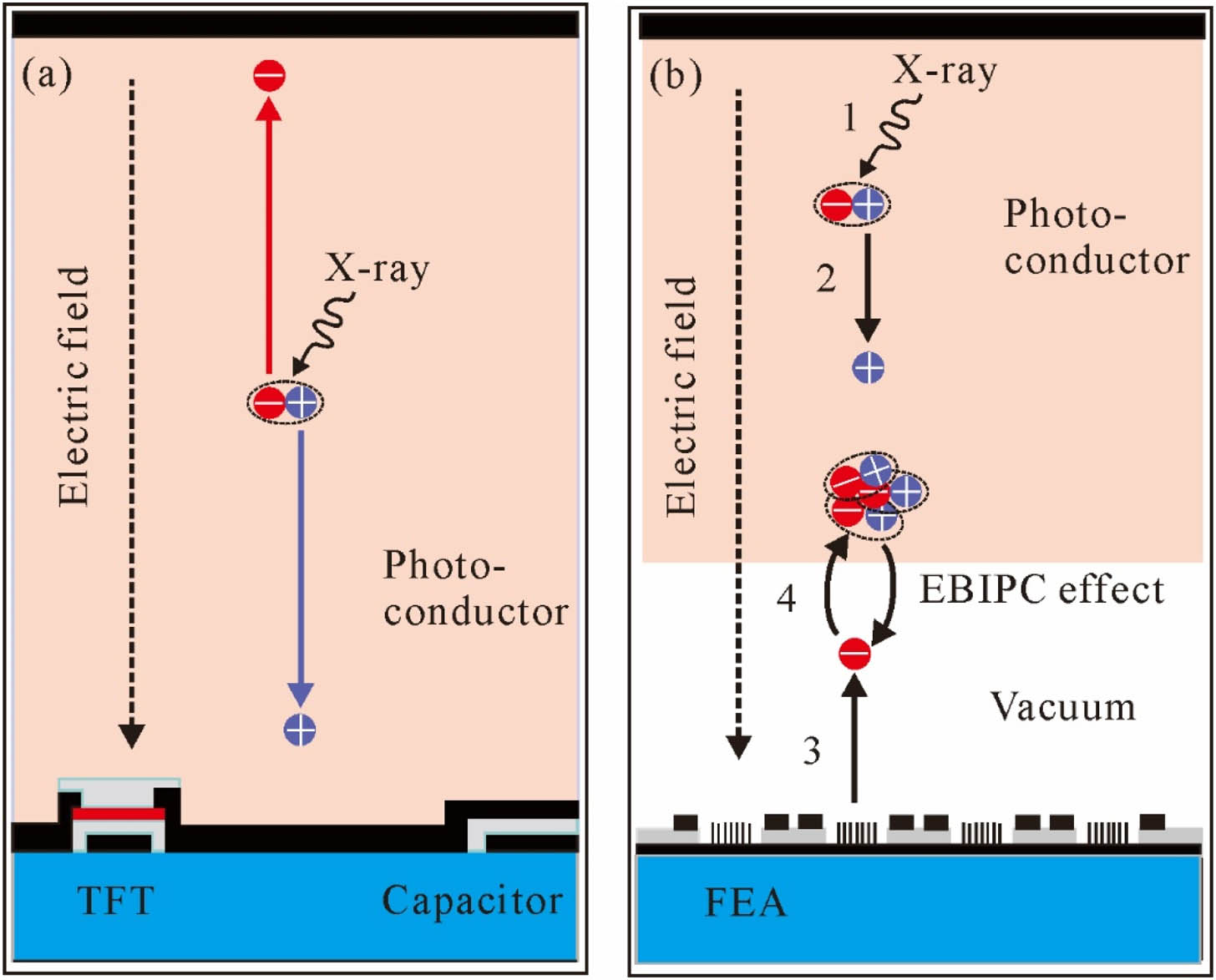
    Fig. 1. Comparison of conceptual design of X-ray detectors and corresponding X-ray response mechanism. (a) Conventional X-ray detectors with TFT readout. (b) Proposed X-ray detectors with vacuum FEA readout.
    Implementation and characterizations of the X-ray detectors. (a) Schematic layout of the vacuum cold cathode X-ray detector. (b) Actual picture of the fabricated X-ray detector. (c) Arrays of patterned ZnO NWs (top image) and cross-sectional view of ZnO NWs (bottom image). (d) Field emission J-E curve of the ZnO NWs with inset showing the corresponding F-N curve. (e) Typical XRD pattern of β-Ga2O3 bulk photoconductor. (f) Total mass attenuation of X-rays in β-Ga2O3 bulk photoconductor showing the contribution from Compton scattering, photoelectric effect, and pair production and that of a-Se and CsPbBr3 photoconductors.
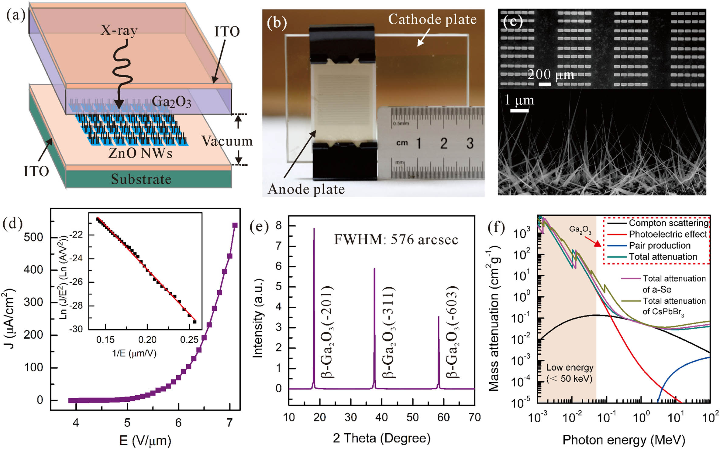
    Fig. 2. Implementation and characterizations of the X-ray detectors. (a) Schematic layout of the vacuum cold cathode X-ray detector. (b) Actual picture of the fabricated X-ray detector. (c) Arrays of patterned ZnO NWs (top image) and cross-sectional view of ZnO NWs (bottom image). (d) Field emission J-E curve of the ZnO NWs with inset showing the corresponding F-N curve. (e) Typical XRD pattern of β-Ga2O3 bulk photoconductor. (f) Total mass attenuation of X-rays in β-Ga2O3 bulk photoconductor showing the contribution from Compton scattering, photoelectric effect, and pair production and that of a-Se and CsPbBr3 photoconductors.
    Detection performance and operation principle of the proposed X-ray detector. (a), (b) Dark current and photocurrent of the X-ray detector at low and high electric fields. (c) F-N curves of the dark current and photocurrent. (d)–(f) Schematic of the operation principle of X-ray detector at different applied electric fields. (g) The detection sensitivity versus applied electric field curves of the X-ray detector. (h) Internal gain versus electric field curve of the detector under X-ray illumination with the X-ray tube voltage of 6 kV and the X-ray tube current of 0.6 mA. (i) The detection sensitivity versus X-ray tube voltage curves of the X-ray detector with inset showing the theoretical determination of detector sensitivity as a function of X-ray energy. (The experimental value was measured using a DC X-ray tube without beam filters.)
    Fig. 3. Detection performance and operation principle of the proposed X-ray detector. (a), (b) Dark current and photocurrent of the X-ray detector at low and high electric fields. (c) F-N curves of the dark current and photocurrent. (d)–(f) Schematic of the operation principle of X-ray detector at different applied electric fields. (g) The detection sensitivity versus applied electric field curves of the X-ray detector. (h) Internal gain versus electric field curve of the detector under X-ray illumination with the X-ray tube voltage of 6 kV and the X-ray tube current of 0.6 mA. (i) The detection sensitivity versus X-ray tube voltage curves of the X-ray detector with inset showing the theoretical determination of detector sensitivity as a function of X-ray energy. (The experimental value was measured using a DC X-ray tube without beam filters.)
    Temporal response of the X-ray detector. (a)–(c) Time-dependent photocurrent of the X-ray detector with pulsed X-ray source on and off at 5 V μm-1 electric field. (d) The SNRs under different X-ray dose rates with inset showing the temporal responses under different X-ray dose rates.
    Fig. 4. Temporal response of the X-ray detector. (a)–(c) Time-dependent photocurrent of the X-ray detector with pulsed X-ray source on and off at 5  Vμm-1 electric field. (d) The SNRs under different X-ray dose rates with inset showing the temporal responses under different X-ray dose rates.
    X-ray Detector TypePhotomultiplier MechanismLinear Attenuation Coefficient (for 20 keV X-ray, mm1)X-ray Energy Range (keV)Operating Electric Field (Vμm1)Dark Current (pAmm-2)Photocurrent (pAmm2, @X-ray energy, X-ray dose, thickness)Sensitivity (μCGyair1cm2)Internal GainResponse Time (ms)Detection Limit (mGyairs1)Reference
    Ga2O3 driven by cold cathodeEBIPC17.26–5022.51.6×1051.8×105 (50 keV, 22.8  mGyairs1, 0.68 mm)3.0×1032.9×102400.28This work
    Ga2O3None17.230–600.0254.0×1061.8×107 (24 keV, 383  mGyairs1, 1 mm)1.4×10³None1.4×1033.8×102[40]
    a-Se driven by cold cathodeAvalanche effect22.820–401009.090 (80 keV, 1.8nGyairs1, 15 μm)Unknown2.0×10233Unknown[41,42]
    a-SeNone22.820–601010103 (20 keV, unknown, 200 μm)22.5None<335.5×10³[11,43,44]
    Perovskite (CsPbBr3)Photoconductive gain effect26.230–500.012.0×1048.0×104 (30 keV, 140  μGyairs1, 240 μm)5.6×1049.0×103922.2×104[6]
    Perovskite (CsPbBr3)None26.220–600.00510500 (60 keV, 20  μGyairs1, 1 mm)4.1×10³None<0.3<2.2×10⁴[45]
    Table 1. Comparison of Performance Metrics of Direct-Conversion X-ray Detectors Based on Different Photoconductors and Photoelectron Multiplication Mechanisms
    Zhipeng Zhang, Manni Chen, Xinpeng Bai, Kai Wang, Huanjun Chen, Shaozhi Deng, Jun Chen. Sensitive direct-conversion X-ray detectors formed by ZnO nanowire field emitters and β-Ga2O3 photoconductor targets with an electron bombardment induced photoconductivity mechanism[J]. Photonics Research, 2021, 9(12): 2420
    Download Citation