• Photonics Research
  • Vol. 9, Issue 12, 2420 (2021)
Zhipeng Zhang, Manni Chen, Xinpeng Bai, Kai Wang, Huanjun Chen, Shaozhi Deng, and Jun Chen*
Author Affiliations
  • State Key Laboratory of Optoelectronic Materials and Technologies, Guangdong Province Key Laboratory of Display Material and Technology, School of Electronics and Information Technology, Sun Yat-sen University, Guangzhou 510275, China
  • show less
    DOI: 10.1364/PRJ.438204 Cite this Article Set citation alerts
    Zhipeng Zhang, Manni Chen, Xinpeng Bai, Kai Wang, Huanjun Chen, Shaozhi Deng, Jun Chen. Sensitive direct-conversion X-ray detectors formed by ZnO nanowire field emitters and β-Ga2O3 photoconductor targets with an electron bombardment induced photoconductivity mechanism[J]. Photonics Research, 2021, 9(12): 2420 Copy Citation Text show less

    Abstract

    Sensitive X-ray detection is needed in diverse areas motivated by a common desire to reduce radiation dose. Cold cathode X-ray detectors operating with a photoelectron multiplication mechanism called electron bombardment induced photoconductivity (EBIPC) have emerged as promising candidates for low-dose X-ray detection. Herein, the cold cathode detectors formed by ZnO nanowire field emitters and β-Ga2O3 photoconductor targets were proposed for sensitive direct-conversion X-ray detection. The charge carrier transport mechanism of EBIPC effect in X-ray detectors was investigated to achieve a high internal gain (2.9×10²) and high detection sensitivity (3.0×10³ μCGyair-1 cm-2) for a 6 keV X-ray at the electric field of 22.5 V μm-1. Furthermore, the proposed X-ray detectors showed the features of fast response time (40 ms), long-term stability (0.6% for 1 h), and low detection limit (0.28 mGyair s-1), suggesting that the direct-conversion cold cathode X-ray detectors are ideal candidates for low-energy X-ray detecting and imaging applications.

    1. INTRODUCTION

    X-ray has the ability to interact with electrons in the atoms to ionize targeted materials and shows a good dose-dependent feature [1,2]. Therefore, X-ray detection is of great significance for medical imaging, security screening, industrial nondestructive inspection, scientific research, etc. [35]. To meet these applications, high detection sensitivity is crucial for achieving high-contrast images and reducing radiation-related health risks [6,7].

    Typically, two different methods are adopted for X-ray detection. The dominant indirect-conversion X-ray detectors use phosphors or scintillators to transform an X-ray into visible light so the spatial resolution and conversion efficiency are limited [8,9]. In contrast, the direct-conversion X-ray detectors use a semiconductor layer to convert an X-ray directly into electric signals and show the advantages of high spatial resolution, fast response time, and wide linear dynamic range [10,11]. However, the commercial a-Se photoconductor used in direct-conversion X-ray detectors has the drawback of low X-ray absorption coefficient for general radiology applications, resulting in a limited sensitivity of 22.5  μCGyair1cm2 for 20–60 keV X-ray [4,5,11]. In addition, the HgI2 photoconductors are widely applied in X-ray detection owing to the heavy atoms, low electron-hole pair (EHP) production energy (5 eV), and high charge carrier mobility lifetime (μτ) product value (105 to 103  cm2V1); further, the detectors exhibit a high sensitivity of 2.2×10³  μCGyair1cm2 for 26–72 keV X-ray [12,13]. However, the poor device compatibility and thermal stability of HgI2 photoconductors must be addressed before their practical application [14]. Recently, perovskite photoconductors prepared by solution process were introduced and exhibited a high X-ray absorption coefficient that enabled the low-dose X-ray detection [5,15]. The sensitivity of 1.1×10⁴  μCGyair1cm2 (100 keV X-ray) at 0.24  Vμm1 and the response time of 10  ms were reported in polycrystalline CH3NH3PbI3-based X-ray detectors consisting of 1428×1428  pixels with a pixel pitch of 70 μm [5]. However, the ion migration and long-term operation stability problems of perovskite X-ray detectors still limit detector performance [16].

    In addition, the X-ray detection sensitivity can be tremendously improved using the photoelectron multiplication mechanism. There are three main photoelectron multiplication mechanisms for realizing highly sensitive X-ray detection: photoemission and secondary emission in vacuum photomultiplier tubes (PMTs) [17], avalanche multiplication mechanism in avalanche photodiodes (APDs) and pixelated silicon photomultipliers (SiPMs) [18,19], and photoconductive gain in X-ray detectors with electronic injection at high electric field [20]. However, commercial PMTs have a bulky size and high cost; the APDs and SiPMs have drawbacks of temperature-dependent gain and low X-ray absorption coefficient due to material limitation; the X-ray detectors with photoconductor gain suffer from the issue of a current runaway effect that occurs at a high electric field so the gain is limited. Therefore, it is challenging to develop a flat-panel X-ray detector with simple preparation method, high-stability, high X-ray absorption coefficient, and high internal gain.

    In order to develop a flat-panel X-ray detector for highly sensitive and low-dose X-ray detection, vacuum cold cathode flat-panel X-ray detectors have been fabricated successfully in recent years and achieve high internal gain [21,22]. The detectors consist of a-Se high-gain avalanche rushing photoconductors (HARPs) for photoelectric conversion and Spindt-type field emission arrays (FEAs) for signal readout [21]. Those vacuum X-ray detectors achieved a pixel number of 640×480, a spatial resolution of 20 μm, and an avalanche multiplication factor of 200 [22]. However, the realized X-ray sensitivity and effective device area were limited due to material limitation of HARPs and complicated fabrication method of Spindt-type FEAs, making those X-ray detectors far from actual applications. Recently, the vacuum cold cathode flat-panel X-ray detectors consisting of ZnS photoconductor and ZnO nanowire (NW) field emitters with a photoelectron multiplication mechanism called electron-bombardment-induced photoconductivity (EBIPC) were proposed to achieve large-area (4.8  cm×8  cm) and high-gain (104) indirect-conversion X-ray detection [23,24]. Nevertheless, the direct-conversion vacuum cold cathode X-ray detectors operating with an EBIPC mechanism have not been realized, and the corresponding charge transport mechanism requires further investigation.

    Here, the direct-conversion vacuum cold cathode X-ray detectors consisting of ZnO NW field emitters and β-Ga2O3 photoconductor targets were proposed to realize sensitive and low-dose X-ray detection. The ZnO NW field emitters show advantages of simple preparation method, good controllability, large area, and excellent field emission performance [25]. The β-Ga2O3 photoconductors have a wide bandgap of 4.9  eV, a breakdown voltage of 8  MVcm1, a relatively high density (6.44  gcm3), and a high absorption coefficient (17.2  mm1 for 20 keV X-ray) for low-energy X-ray [26]. Those metrics meet the requirement of vacuum cold cathode X-ray detectors with a low dark current and an effective EBIPC effect for achieving high internal gain. In addition, the charge carrier transport mechanism of EBIPC effect in X-ray detectors was investigated to achieve sensitive X-ray detection and low detection limit. These results demonstrate that the direct-conversion vacuum cold cathode X-ray detectors with an EBIPC mechanism can potentially be applied in various X-ray detecting applications.

    2. RESULTS AND DISCUSSION

    Conventional direct-conversion X-ray detectors with thin film transistor (TFT) readout are illustrated in Fig. 1(a) [4]. The EHPs are generated in a photoconductor through the absorption of X-ray photons. Nowadays, a-Se photoconductors used in commercial X-ray detectors have drawbacks of low X-ray absorption efficiency and charge collection efficiency. The developing X-ray detectors based on CdTe [27], PbO [28], HgI2 [12], and perovskite [1] photoconductors have high X-ray absorption coefficient and low EHP production energy to generate adequate EHPs, resulting in a significant improvement of X-ray detection sensitivity. Nevertheless, the reported X-ray detectors lacked sufficient internal gain to overcome the recombination or trapping of EHPs. The architectures of 3D photosensitive TFT based X-ray detectors were proposed to achieve high internal gain of 104; however, those devices raised fabrication complexity and cost [29].

    Comparison of conceptual design of X-ray detectors and corresponding X-ray response mechanism. (a) Conventional X-ray detectors with TFT readout. (b) Proposed X-ray detectors with vacuum FEA readout.

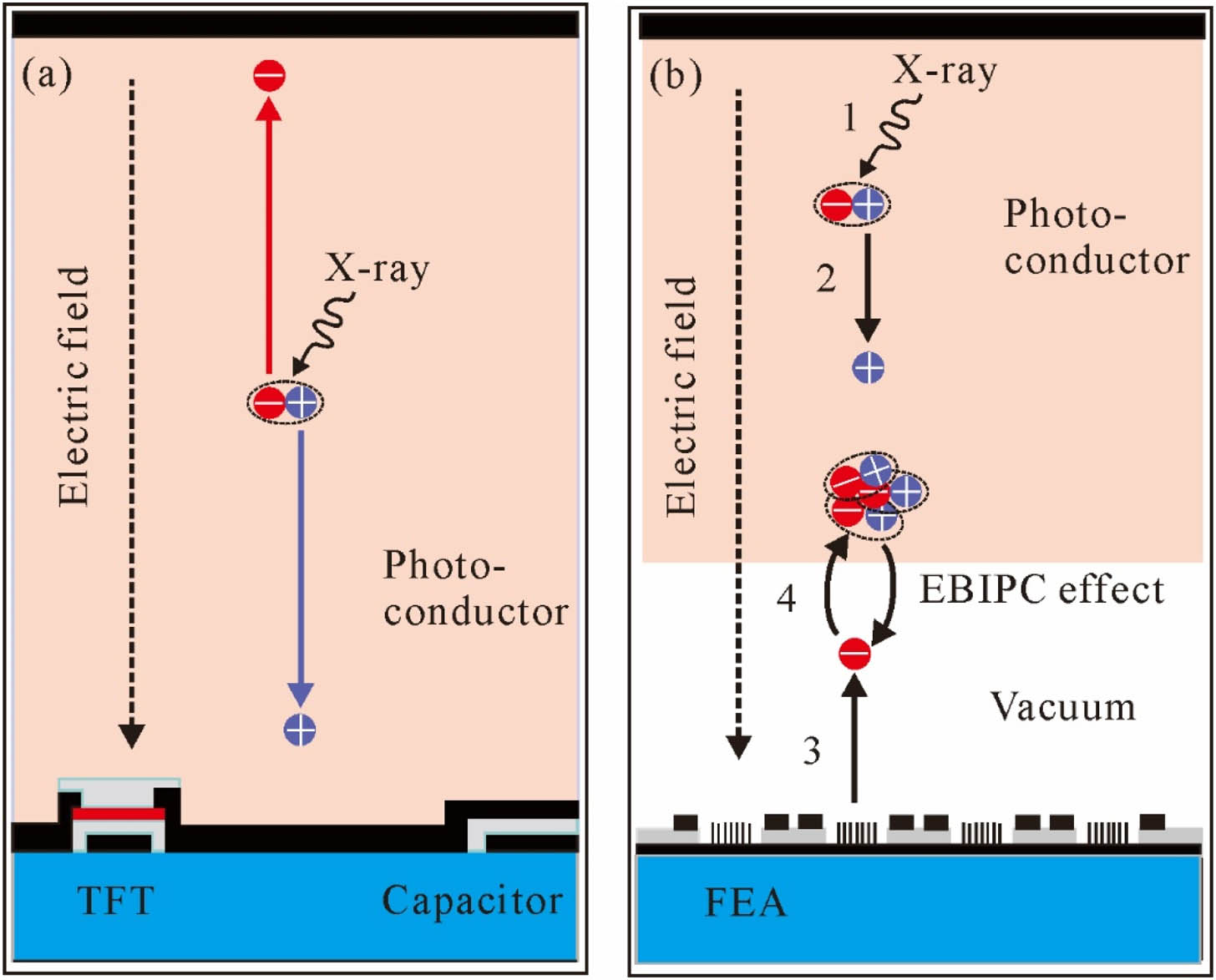
    Figure 1.Comparison of conceptual design of X-ray detectors and corresponding X-ray response mechanism. (a) Conventional X-ray detectors with TFT readout. (b) Proposed X-ray detectors with vacuum FEA readout.

    The proposed device structure formed by gated FEAs and photoconductor target for achieving low dose X-ray imaging is illustrated in Fig. 1(b). These vacuum cold cathode X-ray detectors with high-resolution imaging (20 μm) and high-radiation tolerance (1  MGyairγ-ray) have been demonstrated [30]. In addition, the EHPs in photoconductor can be modulated by both incident photons and accelerated electron emission from a cold cathode, leading to high internal gain. Owing to such high gain effect, the ability of vacuum cold cathode photodetectors to detect ultraweak visible light (100  nWcm2) has been well demonstrated [23]. Therefore, the direct-conversion X-ray detection with high gain can be expected by using vacuum cold cathode detectors. The corresponding X-ray response process of designed X-ray detectors can be divided into four steps: (1) EHPs are generated by incident X-ray photons in the photoconductor layer; (2) the generated EHPs drift across the photoconductor under the electric field; (3) the conductivity of the photoconductor is decreased and causes the electron emission of a cold cathode; (4) the photoconductor is bombarded by the field emission electrons of a cold cathode, and abundant EHPs are generated by the EBIPC effect. The EBIPC effect and field emission of a cold cathode form a positive feedback process until reaching a balance when the voltage dropped in the photoconductor increases at high current. Through this high gain mechanism, internal signal amplification and a highly sensitive X-ray detection can be realized in vacuum cold cathode X-ray detectors. More importantly, the vacuum gap in the proposed X-ray detector can realize a low dark current at high electric field, enabling a low-dose X-ray detection.

    Our device adopts a vacuum photodiode formed by a Ga2O3 photoconductor and ZnO NW field emitters to realize the direct-conversion X-ray detection with an EBIPC mechanism, as illustrated in Fig. 2(a). Figure 2(b) shows an actual photograph of the X-ray detector. The generation rate of EHPs inside the Ga2O3 photoconductor caused by the EBIPC effect strongly depends on the electron beam accelerated voltage and accelerated current emission from the ZnO NWs. Therefore, the photoelectron multiplication factor can be tuned in an X-ray detector using cold cathodes made in forms of addressable FEAs [25].

    Implementation and characterizations of the X-ray detectors. (a) Schematic layout of the vacuum cold cathode X-ray detector. (b) Actual picture of the fabricated X-ray detector. (c) Arrays of patterned ZnO NWs (top image) and cross-sectional view of ZnO NWs (bottom image). (d) Field emission J-E curve of the ZnO NWs with inset showing the corresponding F-N curve. (e) Typical XRD pattern of β-Ga2O3 bulk photoconductor. (f) Total mass attenuation of X-rays in β-Ga2O3 bulk photoconductor showing the contribution from Compton scattering, photoelectric effect, and pair production and that of a-Se and CsPbBr3 photoconductors.

    Figure 2.Implementation and characterizations of the X-ray detectors. (a) Schematic layout of the vacuum cold cathode X-ray detector. (b) Actual picture of the fabricated X-ray detector. (c) Arrays of patterned ZnO NWs (top image) and cross-sectional view of ZnO NWs (bottom image). (d) Field emission J-E curve of the ZnO NWs with inset showing the corresponding F-N curve. (e) Typical XRD pattern of β-Ga2O3 bulk photoconductor. (f) Total mass attenuation of X-rays in β-Ga2O3 bulk photoconductor showing the contribution from Compton scattering, photoelectric effect, and pair production and that of a-Se and CsPbBr3 photoconductors.

    In addition, the charge collection efficiency of the X-ray detector is related to the field emission characteristics of ZnO NWs and the performance metrics of Ga2O3 photoconductors. The top image of Fig. 2(c) shows the actual arrays of ZnO NWs grown on an indium tin oxide (ITO)-coated glass substrate; the bottom image of Fig. 2(c) shows the cross-sectional view of ZnO NWs. The ZnO NWs grown directly on the substrate had a distribution density of 5×10⁸  cm2, a height of 3–4 μm, and a tip diameter of 20  nm. The grown ZnO NWs are reported to have a uniform morphology and are easy to be integrated in gated FEAs, which is beneficial for X-ray imaging applications [25]. Figure 2(d) shows the field emission current density-electric field (J-E) characteristics of ZnO NWs. The grown ZnO NWs with a turn-on field (which corresponds to a current density of 10  μAcm2) of 4.4  Vμm1 showed excellent field emission characteristics compared with previously reported ZnO NWs [31]. The Fowler–Nordheim (F-N) plot [shown in the inset of Fig. 2(d)] was approximately a straight line, indicating that the field emission of ZnO NWs followed the classic vacuum electron tunneling mechanism [32].

    In order to obtain the crystallinity of Ga2O3 photoconductors, the typical X-ray diffraction (XRD) pattern was measured [Fig. 2(e)]. The peaks fitted well with the monoclinic Ga2O3 Joint Committee on Power Diffraction Standards (JCPDS) card No. 43-1012 with the lattice constants of a=12.23, b=3.04, and c=5.8. The peaks located at 18.1°, 37.7°, and 58.5° correspond to the (-201), (311), and (-603) planes. The corresponding full width at half maximum of the XRD peaks of current Ga2O3 was 576 arcsec, which was nearly the same as that of reported Ga2O3 crystal (540 arcsec) prepared by metal–organic chemical vapor deposition method [33]. The XRD results demonstrate the high crystal quality of the Ga2O3 photoconductor, which is beneficial for realizing low dark current, fast response time, and high charge collection efficiency. Figure 2(f) shows the X-ray mass attenuation coefficients of different photoconductors [obtained from the National Institute of Standards and Technology (NIST) database] [34]. On the one hand, the photoelectric effect dominates the total mass attenuation coefficient of the Ga2O3 photoconductor throughout the low-energy X-ray range; on the other hand, the total mass attenuation coefficient of the Ga2O3 photoconductor is close to that of a-Se and CsPbBr3 photoconductors throughout the low-energy X-ray range (<50  keV). Those metrics demonstrate that the Ga2O3 photoconductor is an ideal material for low-energy X-ray detection.

    In addition to exploring the charge transport mechanism of the detector to achieve maximum X-ray detection sensitivity, the dark current and photocurrent were measured at low and high electric fields [Figs. 3(a) and 3(b)]. The nonzero dark current and photocurrent at zero electric field shown in Fig. 3(a) might be caused by the trapped electron in the Ga2O3 crystal due to the electron bombardment. The negatively charged Ga2O3 crystal would release electrons forming a reversed leakage current when we repetitively measured the device. The current-electric field (I-E) characteristics of X-ray detector shown in Fig. 3(b) exhibited three processes: (1) the device current increased gradually until reaching saturation at 1.5  Vμm1; (2) the device current increased slightly at the electric field between 1.5 and 4  Vμm1; (3) the device current increased dramatically after 4  Vμm1. In process (3), the device current (I) can be described using the F-N theory [32]: I=AV2Eφt2(y)exp(BEφ32Vv(y)),where A and B are constants, V is the equivalent voltage in the tip of ZnO NWs, Eϕ is the work function of ZnO NWs, and t(y) and v(y) are the Nordheim elliptic functions. Figure 3(c) shows the F-N plots of dark current and photocurrent in process (3), suggesting that the device current followed the classic electron tunneling mechanism first and then exhibited a saturation feature due to the increasing voltage drop in Ga2O3 photoconductor induced by the high current [23].

    Detection performance and operation principle of the proposed X-ray detector. (a), (b) Dark current and photocurrent of the X-ray detector at low and high electric fields. (c) F-N curves of the dark current and photocurrent. (d)–(f) Schematic of the operation principle of X-ray detector at different applied electric fields. (g) The detection sensitivity versus applied electric field curves of the X-ray detector. (h) Internal gain versus electric field curve of the detector under X-ray illumination with the X-ray tube voltage of 6 kV and the X-ray tube current of 0.6 mA. (i) The detection sensitivity versus X-ray tube voltage curves of the X-ray detector with inset showing the theoretical determination of detector sensitivity as a function of X-ray energy. (The experimental value was measured using a DC X-ray tube without beam filters.)

    Figure 3.Detection performance and operation principle of the proposed X-ray detector. (a), (b) Dark current and photocurrent of the X-ray detector at low and high electric fields. (c) F-N curves of the dark current and photocurrent. (d)–(f) Schematic of the operation principle of X-ray detector at different applied electric fields. (g) The detection sensitivity versus applied electric field curves of the X-ray detector. (h) Internal gain versus electric field curve of the detector under X-ray illumination with the X-ray tube voltage of 6 kV and the X-ray tube current of 0.6 mA. (i) The detection sensitivity versus X-ray tube voltage curves of the X-ray detector with inset showing the theoretical determination of detector sensitivity as a function of X-ray energy. (The experimental value was measured using a DC X-ray tube without beam filters.)

    The operation principle of the X-ray detector is illustrated to further demonstrate the I-E characteristics and X-ray response process at different electric fields. As shown in Figs. 3(d)–3(f), the charge transport mechanism of the X-ray detector can be divided into three regions. In Region I, the internal photoelectric effect of X-ray photons in the Ga2O3 photoconductor dominates at the small electric field. The collected charge increases before reaching saturation at the saturated electric field (Esat), owing to the limited photogenerated carriers in the Ga2O3 photoconductor and high vacuum barrier of the ZnO NWs. In Region II, the charges are injected from the electrodes when the charge recombination lifetime is larger than the charge transit time at a higher electric field, which triggers a photoconductive gain [20]. The device current increases slightly in this region, but the total collected charge is still limited by the large vacuum barrier of ZnO NWs. In Region III, the EBIPC effect occurs when the Ga2O3 photoconductor is bombarded by the high-energy accelerated electrons emission from ZnO NWs at a high electric field (Eb). Under the EBIPC effect, the conductivity of a Ga2O3 photoconductor becomes smaller, and the vacuum barrier of ZnO NWs becomes lower and narrower, making the photocurrent increase dramatically; further, the collected photogenerated charge is amplified eventually.

    Under the EBIPC mechanism, the X-ray detector achieved high detection sensitivity. Calculated from the X-ray responsive J-E curves of the metal-semiconductor-metal-structured Ga2O3 X-ray detector, the resistivity of the Ga2O3 photoconductor decreased from 8.6×10¹¹  Ωcm to 3.4×10¹¹  Ωcm after the illumination of 50 keV X-ray. According to the field emission J-E curve of the ZnO NWs [Fig. 2(d)] and X-ray responsive J-E curve of the proposed vacuum cold cathode X-ray detector, the bias variation of ZnO NWs was 0.08  Vμm1 after the illumination of 50 keV X-ray, making resistivity of the Ga2O3 photoconductor become 6.2×10¹⁰  Ωcm, owing to the bombardment of accelerated electrons with higher energy. Figure 3(g) shows the X-ray detection sensitivities as a function of an applied electric field under different X-ray tube voltages. The sensitivity increased quickly with the increasing applied electric field of the detector owing to the high generation rates of EHPs in Ga2O3 photoconductor at high electric field, and then the sensitivity saturated at a higher applied electric field due to a balance between the accelerated voltage of field emission and bias voltage of the Ga2O3 photoconductor. The maximum sensitivity of the X-ray detector was 3.0×10³  μCGyair1cm2 (the applied electric field was 22.5  Vμm1) under the X-ray tube voltage of 6 kV. The realized X-ray detection sensitivity was much higher than that of the metal-semiconductor-metal-structured Ga2O3 X-ray detector with the maximum sensitivity of 63  μCGyair1cm2 (6 keV X-ray), exhibiting the high internal gain of vacuum cold cathode X-ray detectors with EBIPC mechanism. The internal gain (G) of the X-ray detector can be described as [10] G=IRIP=IRφβe,where IR and IP=φβe stand for the experimental current and theoretical photogenerated current of detector under X-ray illumination, in which φ=εDmsEph is the photon absorption rate and β=EphW± is the number of carriers excited by an X-ray photon. Notably, e is an electronic charge, ε is the fraction of absorbed photons [this value is nearly 100% in 0.68 mm Ga2O3 photoconductor for low-energy (1–20 keV) X-ray calculated from the NIST database] [34], D is the X-ray dose rate, ms is the mass of Ga2O3 photoconductor, Eph is the X-ray energy, and W±=2.7Eg+Ephonon is the EHP production energy [11], where Eg=4.9  eV is the bandgap of the Ga2O3 photoconductor and Ephonon=29  meV is the phonon energy of Ga2O3 photoconductor [35]. The calculated internal gain of an X-ray detector up to 2.9×10² at 22.5  Vμm1 electric field is achieved [Fig. 3(h)], demonstrating that the EBIPC mechanism is promising for use in sensitive X-ray detectors with high internal gain.

    Figure 3(i) shows the X-ray detection sensitivity under different X-ray tube voltages measured by a DC X-ray tube without beam filters. The sensitivity decreased quickly from 1.2×10³ to 0.3  μCGyair1cm2 when the X-ray tube voltage increased from 6 to 50 kV at 10  Vμm1, indicating that the Ga2O3-based vacuum cold cathode X-ray detectors are suitable for low-energy X-ray detection owing to the high absorption efficiency of the Ga2O3 photoconductor for low-energy X-ray. The detection sensitivity (S) can be theoretically described as [36,37] S=GCeΨαen(1exp(αT))W±,where C is the charge collection efficiency, Ψ is the incident radiant energy flux density, αen is the energy absorption coefficient of Ga2O3, α is the linear attenuation coefficient of Ga2O3, and T is the thickness of Ga2O3. According to Eq. (3), the sensitivity is mainly dominated by the energy absorption coefficient and linear attenuation coefficient of the Ga2O3 photoconductor under different X-ray energies. The simulated detection sensitivity as a function of X-ray energy using Eq. (3) is shown in the inset of Fig. 3(i), showing good agreement with the experimental results.

    Typical temporal responses of the X-ray detectors at the electric field of 5  Vμm1 were tested with X-ray square-waves (the dose rate is 17.9  mGyairs1), as displayed in Figs. 4(a)–4(c). The fluctuation (F) of the photocurrent is calculated using F=(I2I1)/I1, where I1 is the average photocurrent of the first pulse and I2 is the average photocurrent of the last pulse. The fluctuations in the photocurrent were 0.4% over 170 s [Fig. 4(a)] and 0.6% over a 1 h period [Fig. 4(c)], indicating that the proposed X-ray detectors have an excellent stability owing to the high crystal quality of the Ga2O3 photoconductor and current limitation of the vacuum gap. The rise and fall times (the time for the transit between 10% and 90% of the photocurrent) were calculated to be 140 and 40 ms, respectively. The response time of proposed X-ray detectors is much faster than that of the previously reported Ga2O3-based X-ray detector (1.8 s) [38], which is mainly caused by the fast charge transport speed in the high-crystallinity Ga2O3 photoconductor and vacuum gap. The realized response speed is fully adequate for radiography applications requiring a readout time of less than 5 s [1]. In addition, Fig. 4(d) shows the signal-to-noise ratios (SNRs) [39] under different X-ray dose rates at the electric field of 5  Vμm1; the inset of Fig. 4(d) shows the corresponding temporal responses under different X-ray dose rates. The SNR of X-ray detector increased from 0.9 to 64.8 when the radiation dose rate increased from 1.2×10³ to 38.1  mGyairs1. The SNR showed a saturation feature under the illumination of a low-dose X-ray (<0.1  mGyairs1) due to the measured current noise [as shown in the inset of Fig. 4(d)], which could be increased by adopting more sophisticated electrostatic shielding and cable. The corresponding detection limit (according to the IUPAC standard of SNR of 3) [39] was as low as 0.28  mGyairs1, exhibiting a large improvement compared with that of the reported Ga2O3 based X-ray detector (140  mGyairs1) [38].

    Temporal response of the X-ray detector. (a)–(c) Time-dependent photocurrent of the X-ray detector with pulsed X-ray source on and off at 5 V μm-1 electric field. (d) The SNRs under different X-ray dose rates with inset showing the temporal responses under different X-ray dose rates.

    Figure 4.Temporal response of the X-ray detector. (a)–(c) Time-dependent photocurrent of the X-ray detector with pulsed X-ray source on and off at 5  Vμm-1 electric field. (d) The SNRs under different X-ray dose rates with inset showing the temporal responses under different X-ray dose rates.

    The performance metrics of the proposed X-ray detector and literature-reported direct-conversion X-ray detectors using different photoconductors and photoelectron multiplication mechanisms are compared in Table 1. The proposed X-ray detectors formed by photoconductor targets and cold cathode field emitters can achieve high internal gain using the EBIPC mechanism. The Ga2O3 photoconductor is an ideal material for a vacuum cold cathode X-ray detector owing to its high absorption efficiency for a low-energy X-ray and high breakdown electric field to operate at a high electric field. Under the EBIPC mechanism, the proposed X-ray detector realized a high internal gain of 2.9×10², a high X-ray detection sensitivity of 3.0×10³  μCGyair1cm2 for 650  keV X-ray, and a low detection limit of 0.28  mGyairs1. Furthermore, the detector achieved a fast response time of 40 ms owing to the high crystal quality of the Ga2O3 photoconductor and fast charge transport speed in the vacuum gap. The performance metrics of the proposed X-ray detectors are much better than those of the literature-reported Ga2O3-based X-ray detectors without a photoelectron multiplication mechanism [40]. In contrast, the vacuum cold cathode X-ray detectors formed by HARPs and Spindt-type FEAs had a high internal gain (2.0×10²) and were expected to realize low-dose X-ray imaging using the avalanche effect [41,42]. However, those detectors have limited X-ray detection sensitivity due to the material limitation of HARPs and are not eligible for large area applications due to the complicated fabrication method of Spindt-type FEAs. Furthermore, the a-Se-based X-ray detectors without photoelectron multiplication mechanism had the drawback of low X-ray absorption coefficient for general radiology applications, resulting in a limited sensitivity of 22.5  μCGyair1cm2 for 20–60 keV X-ray [11,43,44]. In addition, the perovskite photoconductors had high X-ray absorption coefficient and high charge collection efficiency, benefiting to realize high X-ray detection sensitivity (4.1×10³  μCGyair1cm2 for 20–60 keV X-ray) and low detection limit (0.22  μGyairs1) [45]. Furthermore, the perovskite based X-ray detectors could realize a higher detection sensitivity (5.6×10⁴  μCGyair1cm2 for 30–50 keV X-ray) using the photoconductive gain effect and a fast response time (<0.3  ms) by applying a photoconductor with high crystal quality [6,45]. Nevertheless, the issues of ion migration and long-term operation stability make the perovskite-based X-ray detectors far from practical applications [16].

    Comparison of Performance Metrics of Direct-Conversion X-ray Detectors Based on Different Photoconductors and Photoelectron Multiplication Mechanisms

    X-ray Detector TypePhotomultiplier MechanismLinear Attenuation Coefficient (for 20 keV X-ray, mm1)X-ray Energy Range (keV)Operating Electric Field (Vμm1)Dark Current (pAmm-2)Photocurrent (pAmm2, @X-ray energy, X-ray dose, thickness)Sensitivity (μCGyair1cm2)Internal GainResponse Time (ms)Detection Limit (mGyairs1)Reference
    Ga2O3 driven by cold cathodeEBIPC17.26–5022.51.6×1051.8×105 (50 keV, 22.8  mGyairs1, 0.68 mm)3.0×1032.9×102400.28This work
    Ga2O3None17.230–600.0254.0×1061.8×107 (24 keV, 383  mGyairs1, 1 mm)1.4×10³None1.4×1033.8×102[40]
    a-Se driven by cold cathodeAvalanche effect22.820–401009.090 (80 keV, 1.8nGyairs1, 15 μm)Unknown2.0×10233Unknown[41,42]
    a-SeNone22.820–601010103 (20 keV, unknown, 200 μm)22.5None<335.5×10³[11,43,44]
    Perovskite (CsPbBr3)Photoconductive gain effect26.230–500.012.0×1048.0×104 (30 keV, 140  μGyairs1, 240 μm)5.6×1049.0×103922.2×104[6]
    Perovskite (CsPbBr3)None26.220–600.00510500 (60 keV, 20  μGyairs1, 1 mm)4.1×10³None<0.3<2.2×10⁴[45]

    3. CONCLUSIONS

    In summary, a direct-conversion vacuum cold cathode X-ray detector based on ZnO NW field emitters and β-Ga2O3 photoconductor targets was proposed to realize sensitive and low-dose X-ray detection. The charge carrier transport mechanism of the X-ray detectors was investigated, finding that the X-ray response process could be divided into internal photoelectric effect, photoconductive gain effect, and EBIPC effect when the applied electric field increased accordingly. The proposed X-ray detectors operating with an EBIPC mechanism achieved a high internal gain of 2.9×10² and high detection sensitivity up to 3.0×10³  μCGyair1cm2 for 6 keV X-ray at the 22.5  Vμm1 electric field. Moreover, the direct-conversion vacuum cold cathode X-ray detector also had the advantages of fast response time, long-term stability, and low detection limit owing to the high crystal quality of the Ga2O3 photoconductor and current limitation effect of the vacuum gap. The proposed direct-conversion vacuum cold cathode X-ray detectors demonstrate huge potential for use in actual X-ray detection applications.

    APPENDIX A: METHODS

    Fabrication of a Vacuum Cold Cathode X-ray Detector

    A vacuum diode-type cold cathode X-ray detector was fabricated with the ZnO NW field emitters as the cathode and the β-Ga2O3 photoconductor as the anode target. The arrays of patterned ZnO NWs were directly grown on an ITO-coated glass substrate using a thermal oxidation method [25]. First, a 500 nm thick ITO electrode was deposited on glass substrate by magnetron sputtering. Second, the patterned Zn film with the thickness of 1.2 μm was prepared by ultraviolet lithography and electron beam evaporation. Last, the ZnO NWs were grown by oxidating the patterned Zn film with air in a horizontal quartz tube furnace. The oxidation temperature was 500°C; the oxidation time was 3 h. The single dot matrix size of ZnO NWs was 25  μm×60  μm, and the duty ratio of that was 10.2%. The (-201) Fe-doped β-Ga2O3 bulk photoconductor with 0.68 mm thickness was prepared using an edge-defined film-fed growth method (Novel Crystal Technology Inc., Japan) [46]. The ITO thin film with 200 nm thickness was deposited on the β-Ga2O3 surface to act as an anode electrode using a direct current magnetron sputtering method. The vacuum gap between the Ga2O3 crystal and the patterned ZnO NW cold cathode was maintained by the ceramic spacer; the number of adopted ceramic spacers depended on the area of the detector. The vacuum gap between the anode and cathode was 120 μm. The effective detection area of X-ray detector was 2  cm×2  cm.

    Characterization Methods

    The morphologies of arrays of ZnO NWs were observed using a scanning electron microscope (SEM, SUPRA 60, Germany). Crystallinity of the β-Ga2O3 photoconductor was identified by the XRD (Empyrean, PANalytical B.V) measurement. The X-ray detector operates in a vacuum chamber with a pressure of 5×10⁶  Pa. The proposed flat panel X-ray detectors can be sealed using a glass frit with sintering process and pumped to high vacuum (<1×10⁵  Pa) before being sealed off [47,48]. A commercial X-ray tube with a tungsten target and 50 kV maximum accelerated voltage was used as the X-ray source (Vision Imaging Technology Limited). The radiation dose rates under different X-ray tube voltages were calibrated using a commercial dosimeter (MagicMax XM detector, IBA). The I-E and temporal characteristics of the X-ray detectors were measured using a Keithley 2657A source-meter unit with a maximum applied voltage of 3000 V.

    References

    [1] Z. Z. Li, F. G. Zhou, H. H. Yao, Z. P. Ci, Z. Yang, Z. W. Jin. Halide perovskites for high-performance X-ray detector. Mater. Today, 48, 155-175(2021).

    [2] G. Kakavelakis, M. Gedda, A. Panagiotopoulos, E. Kymakis, T. D. Anthopoulos, K. Petridis. Metal halide perovskites for high‐energy radiation detection. Adv. Sci., 7, 2002098(2020).

    [3] M. Yaffe, J. Rowlands. X-ray detectors for digital radiography. Phys. Med. Biol., 42, 1-39(1997).

    [4] S. Kasap, J. B. Frey, G. Belev, O. Tousignant, H. Mani, J. Greenspan, L. Laperriere, O. Bubon, A. Reznik, G. DeCrescenzo, K. S. Karim, J. A. Rowlands. Amorphous and polycrystalline photoconductors for direct conversion fat panel X-ray image sensors. Sensors, 11, 5112-5157(2011).

    [5] Y. C. Kim, K. H. Kim, D. Son, D. Jeong, J. Seo, Y. S. Choi, I. T. Han, S. Y. Lee, N. Park. Printable organometallic perovskite enables large-area, low-dose X-ray imaging. Nature, 550, 87-91(2017).

    [6] W. Pan, B. Yang, G. Niu, K. Xue, X. Du, L. Yin, M. Zhang, H. Wu, X. Miao, J. Tang. Hot-pressed CsPbBr3 quasi-monocrystalline film for sensitive direct X-ray detection. Adv. Mater., 31, 1904405(2019).

    [7] B. Sinnott, E. Ron, A. B. Schneider. Exposing the thyroid to radiation: a review of its current extent, risks, and implications. Endocr. Rev., 31, 756-773(2010).

    [8] R. T. Williams, W. W. Wolszczak, X. Yan, D. L. Carroll. Perovskite quantum-dot-in-host for detection of ionizing radiation. ACS Nano, 14, 5161-5169(2020).

    [9] X. Y. Liu, G. Pilania, A. A. Talapatra, C. R. Stanek, B. P. Uberuaga. Band-edge engineering to eliminate radiation-induced defect states in perovskite scintillators. ACS Appl. Mater. Interfaces, 12, 46296-46305(2020).

    [10] Y. Zhang, Y. Liu, Z. Xu, H. Ye, Z. Yang, J. You, M. Liu, Y. He, M. G. Kanatzidis, S. Liu. Nucleation-controlled growth of superior lead-free perovskite Cs3Bi2I9 single-crystals for high-performance X-ray detection. Nat. Commun., 11, 2304(2020).

    [11] S. O. Kasap. X-ray sensitivity of photoconductors: application to stabilized a-Se. J. Phys. D, 33, 2853-2865(2000).

    [12] S. O. Kasap, M. Z. Kabir, J. A. Rowlands. Recent advances in X-ray photoconductors for direct conversion X-ray image detectors. Curr. Appl. Phys., 6, 288-292(2006).

    [13] Z. Su, L. E. Antonuk, M. Y. El, L. Hu, H. Du, A. Sawant, Y. Li, Y. Wang, J. Yamamoto, Q. Zhao. Systematic investigation of the signal properties of polycrystalline HgI2 detectors under mammographic, radiographic, fluoroscopic and radiotherapy irradiation conditions. Phys. Med. Biol., 50, 2907-2928(2005).

    [14] Z. P. Zhang, Z. J. Zhang, W. Zheng, K. Wang, H. J. Chen, S. Z. Deng, F. Huang, J. Chen. Sensitive and fast direct conversion X-ray detectors based on single-crystalline HgI2 photoconductor and ZnO nanowire vacuum diode. Adv. Mater. Technol., 5, 1901108(2020).

    [15] J. Zhao, L. Zhao, Y. Deng, X. Xiao, Z. Ni, J. Huang. Perovskite-filled membranes for flexible and large-area direct-conversion X-ray detector array. Nat. Photonics, 14, 612-617(2020).

    [16] B. Yang, W. Pan, H. Wu, G. Niu, J. Yuan, K. Xue, L. Yin, X. Du, X. Miao, X. Yang, Q. Xie, J. Tang. Heteroepitaxial passivation of Cs2AgBiBr6 wafers with suppressed ionic migration for X-ray imaging. Nat. Commun., 10, 1989(2019).

    [17] J. Xie, M. Chiu, E. May, Z. E. Meziani, S. Nelson, R. Wagner. MCP-PMT development at Argonne for particle identification. J. Instrum., 15, C04038(2020).

    [18] B. Chen, Y. Wan, Z. Xie, J. Huang, N. Zhang, C. Shang, J. Norman, Q. Li, Y. Tong, K. M. Lau, A. C. Gossard, J. E. Bowers. Low dark current high gain InAs quantum dot avalanche photodetectors monolithically grown on Si. ACS Photon., 7, 528-533(2020).

    [19] F. A. Ruffinatti, S. Lomazzi, L. Nardo, R. Santoro, A. Martemiyanov, M. Dionisi, L. Tapella, A. A. Genazzani, D. Lim, C. Distasi, M. Caccia. Assessment of a silicon-photomultiplier-based platform for the measurement of intracellular calcium dynamics with targeted aequori. ACS Sens., 5, 2388-2397(2020).

    [20] D. Rui, Y. Fang, J. Chae, J. Dai, Z. Xiao, Q. Dong, Y. Yuan, A. Centrone, C. Z. Xiao, J. Huang. High-gain and low-driving-voltage photodetectors based on organolead triiodide perovskites. Adv. Mater., 27, 1912-1918(2015).

    [21] Y. Honda, M. Nanba, K. Miyakawa, M. Kubota, M. Nagao, Y. Neo, H. Mimura, N. Egami. Double-gated, Spindt-type field emitter with improved electron beam extraction. IEEE Trans. Electron Dev., 63, 2182-2189(2016).

    [22] T. Miyoshi, N. Igarashi, N. Matsugaki, Y. Yamada, K. Hirano, K. Hyodo, K. Tanioka, N. Egami, M. Namba, M. Kubota, T. Kawai, S. Wakatsuki. Development of an X-ray HARP–FEA detector system for high-throughput protein crystallography. J. Synchrotron Radiat., 15, 281-284(2008).

    [23] Z. P. Zhang, K. Wang, K. S. Zheng, S. Z. Deng, N. S. Xu, J. Chen. Electron bombardment induced photoconductivity and high gain in a flat panel photodetector based on a ZnS photoconductor and ZnO nanowire field emitters. ACS Photon., 5, 4147-4155(2018).

    [24] X. P. Bai, Z. P. Zhang, M. N. Chen, K. Wang, J. C. She, S. Z. Deng, J. Chen. Theoretical analysis and verification of electron-bombardment-induced photoconductivity in vacuum flat-panel detector. J. Lightwave Technol., 39, 2618-2624(2021).

    [25] Y. F. Li, Z. P. Zhang, G. F. Zhang, L. Zhao, S. Z. Deng, N. S. Xu, J. Chen. Optimizing the field emission properties of ZnO nanowire arrays by precisely tuning the population density and application in large-area gated field emitter array. ACS Appl. Mater. Interfaces, 9, 3911-3921(2017).

    [26] X. Chen, F. Ren, S. Gu, J. Ye. Review of gallium-oxide-based solar-blind ultraviolet photodetectors. Photon. Res., 7, 381-415(2019).

    [27] J. Tanguay, I. A. Cunningham. Cascaded systems analysis of charge sharing in cadmium telluride photon‐counting X-ray detectors. Med. Phys., 45, 1926-1941(2018).

    [28] G. Benassi, N. Zambelli, M. Villani, D. Calestani, M. Pavesi, A. Zappettini, L. Zanotti, C. Paorici. Oriented orthorhombic lead oxide film grown by vapour phase deposition for X-ray detector applications. Cryst. Res. Technol., 48, 245-250(2013).

    [29] Y. B. Xu, Q. Zhou, J. Huang, W. W. Li, J. Chen, K. Wang. Highly-sensitive indirect-conversion X-ray detector with an embedded photodiode formed by a three-dimensional dual-gate thin-film transistor. J. Lightwave Technol., 38, 3775-3780(2020).

    [30] Y. Gotoh, H. Tsuji, M. Nagao, T. Masuzawa, Y. Neo, H. Mimura, T. Okamoto, T. Igari, M. Akiyoshi, N. Sato, I. Takagi. Development of a field emission image sensor tolerant to gamma-ray irradiation. IEEE Trans. Electron Dev., 67, 1660-1665(2020).

    [31] S. J. Young, Y. L. Chu. Characteristics of field emitters on the basis of Pd-adsorbed ZnO nanostructures by photochemical method. ACS Appl. Nano Mater., 4, 2515-2521(2021).

    [32] R. H. Fowler, L. W. Nordheim. Electron emission in intense electric fields. Proc. R. Soc. London A, 119, 173-181(1928).

    [33] Z. Chen, Z. Li, Y. Zhuo, W. Chen, X. Ma, Y. Pei, G. Wang. Layer-by-layer growth of ε-Ga2O3 thin film by metal-organic chemical vapor deposition. Appl. Phys. Express, 11, 101101(2018).

    [34] M. J. Berger, J. H. Hubbell, S. M. Seltzer, J. Chang, J. S. Coursey, R. Sukumar, D. S. Zucker, K. Olsen. XCOM Phot. Cross Sect. Database (Version 1.5)(2010).

    [35] K. A. Mengle, E. Kioupakis. Vibrational and electron-phonon coupling properties of β-Ga2O3 from first-principles calculations: impact on the mobility and breakdown field. AIP Adv., 9, 015313(2019).

    [36] S. Tie, W. Zhao, D. Xin, M. Zhang, J. D. Long, Q. Chen, X. J. Zheng, J. Zhu, W. H. Zhang. Robust fabrication of hybrid lead-free perovskite pellets for stable X-ray detectors with low detection limit. Adv. Mater., 32, 2001981(2020).

    [37] Z. P. Zhang, Z. M. Chen, M. N. Chen, K. Wang, H. J. Chen, S. Z. Deng, G. Hang, J. Chen. ε-Ga2O3 thin film avalanche low-energy X-ray detectors for highly sensitive detection and fast-response applications. Adv. Mater. Technol., 6, 2001094(2021).

    [38] H. Liang, S. Cui, R. Su, P. Guan, Y. He, L. Yang, L. Chen, Y. Zhang, Z. Mei, X. Du. Flexible X-ray detectors based on amorphous Ga2O3 thin films. ACS Photon., 6, 351-359(2019).

    [39] W. Pan, H. Wu, J. Luo, Z. Deng, C. Ge, C. Chen, X. Jiang, W. J. Yin, G. Niu, L. Zhu, L. Yin, Y. Zhou, Q. Xie, X. Ke, M. Sui, J. Tang. Cs2AgBiBr6 single-crystal X-ray detectors with a low detection limit. Nat. Photonics, 11, 726-732(2017).

    [40] X. Lu, L. D. Zhou, L. Chen, X. P. Ouyang, H. Tang, B. Liu, J. Xu. X-ray detection performance of vertical Schottky photodiodes based on a bulk β-Ga2O3 substrate grown by an EFG method. ECS J. Solid State Sci. Technol., 8, Q3046-Q3049(2019).

    [41] D. A. Scaduto, A. R. Lubinsky, J. A. Rowlands, H. Kenmotsu, N. Nishimoto, T. Nishino, K. Tanioka, Z. Wei. Investigation of spatial resolution and temporal performance of SAPHIRE (scintillator avalanche photoconductor with high resolution emitter readout) with integrated electrostatic focusing. Proc. SPIE, 9033, 90333S(2014).

    [42] T. Masuzawa, I. Saito, T. Yamada, M. Onishi, H. Y. Yamaguchi, K. Oonuki, N. Kato, S. Ogawa, Y. Takakuwa, A. T. T. Koh, D. H. C. Chua, Y. Mori, T. Shimosawa, K. Okano. Development of an amorphous selenium-based photodetector driven by a diamond cold cathode. Sensors, 13, 13744-13778(2013).

    [43] S. Abbaszadeh, C. C. Scott, O. Bubon, A. Reznik, K. S. Karim. Enhanced detection efficiency of direct conversion X-ray detector using polyimide as hole-blocking layer. Sci. Rep., 3, 3360(2013).

    [44] B. Zhao, W. Zhao. Temporal performance of amorphous selenium mammography detectors. Med. Phys., 32, 128-136(2005).

    [45] J. L. Peng, C. Q. Xia, Y. L. Xu, R. M. Li, L. H. Cui, J. K. Clegg, L. M. Herz, M. B. Johnston, Q. Q. Lin. Crystallization of CsPbBr3 single crystals in water for X-ray detection. Nat. Commun., 12, 1531(2021).

    [46] A. Kuramata, K. Koshi, S. Watanabe, Y. Yamaoka, T. Masui, S. Yamakoshi. High-quality β-Ga2O3 single crystals grown by edge-defined film-fed growth. Jpn. J. Appl. Phys., 55, 1202A2(2016).

    [47] X. Q. Cao, G. F. Zhang, Y. Y. Zhao, Y. Xu, J. C. She, S. Z. Deng, N. S. Xu, J. Chen. Fully vacuum-sealed addressable nanowire cold cathode flat-panel X-ray source. Appl. Phys. Lett., 119, 053501(2021).

    [48] D. K. Chen, Y. Xu, G. F. Zhang, Z. P. Zhang, J. C. She, S. Z. Deng, N. S. Xu, J. Chen. A double-sided radiating flat-panel X-ray source using ZnO nanowire field emitters. Vacuum, 144, 266-271(2017).

    Zhipeng Zhang, Manni Chen, Xinpeng Bai, Kai Wang, Huanjun Chen, Shaozhi Deng, Jun Chen. Sensitive direct-conversion X-ray detectors formed by ZnO nanowire field emitters and β-Ga2O3 photoconductor targets with an electron bombardment induced photoconductivity mechanism[J]. Photonics Research, 2021, 9(12): 2420
    Download Citation