• Photonics Research
  • Vol. 10, Issue 6, 1338 (2022)
Xiangwen Guo1, Linbo Shao2, Lingyan He3, Kevin Luke3, Jesse Morgan1, Keye Sun1, Junyi Gao1, Ta-Ching Tzu1, Yang Shen1, Dekang Chen1, Bingtian Guo1, Fengxin Yu1, Qianhuan Yu1, Masoud Jafari1, Marko Lončar2, Mian Zhang3, and Andreas Beling1、*
Author Affiliations
  • 1Department of Electrical and Computer Engineering, University of Virginia, Charlottesville, Virginia 22903, USA
  • 2John A. Paulson School of Engineering and Applied Sciences, Harvard University, Cambridge, Massachusetts 02138, USA
  • 3HyperLight Corporation, Cambridge, Massachusetts 02139, USA
  • show less
    DOI: 10.1364/PRJ.455969 Cite this Article Set citation alerts
    Xiangwen Guo, Linbo Shao, Lingyan He, Kevin Luke, Jesse Morgan, Keye Sun, Junyi Gao, Ta-Ching Tzu, Yang Shen, Dekang Chen, Bingtian Guo, Fengxin Yu, Qianhuan Yu, Masoud Jafari, Marko Lončar, Mian Zhang, Andreas Beling. High-performance modified uni-traveling carrier photodiode integrated on a thin-film lithium niobate platform[J]. Photonics Research, 2022, 10(6): 1338 Copy Citation Text show less
    MUTC PDs integrated on TFLN. (a) Structural illustration. (b) Epitaxial structure of the n-down PD. (c) TFLN waveguide cross section. (d) Microscope image of a device under test with a lensed fiber and a radio frequency probe. (e) Microscope image of chip with integrated PDs.
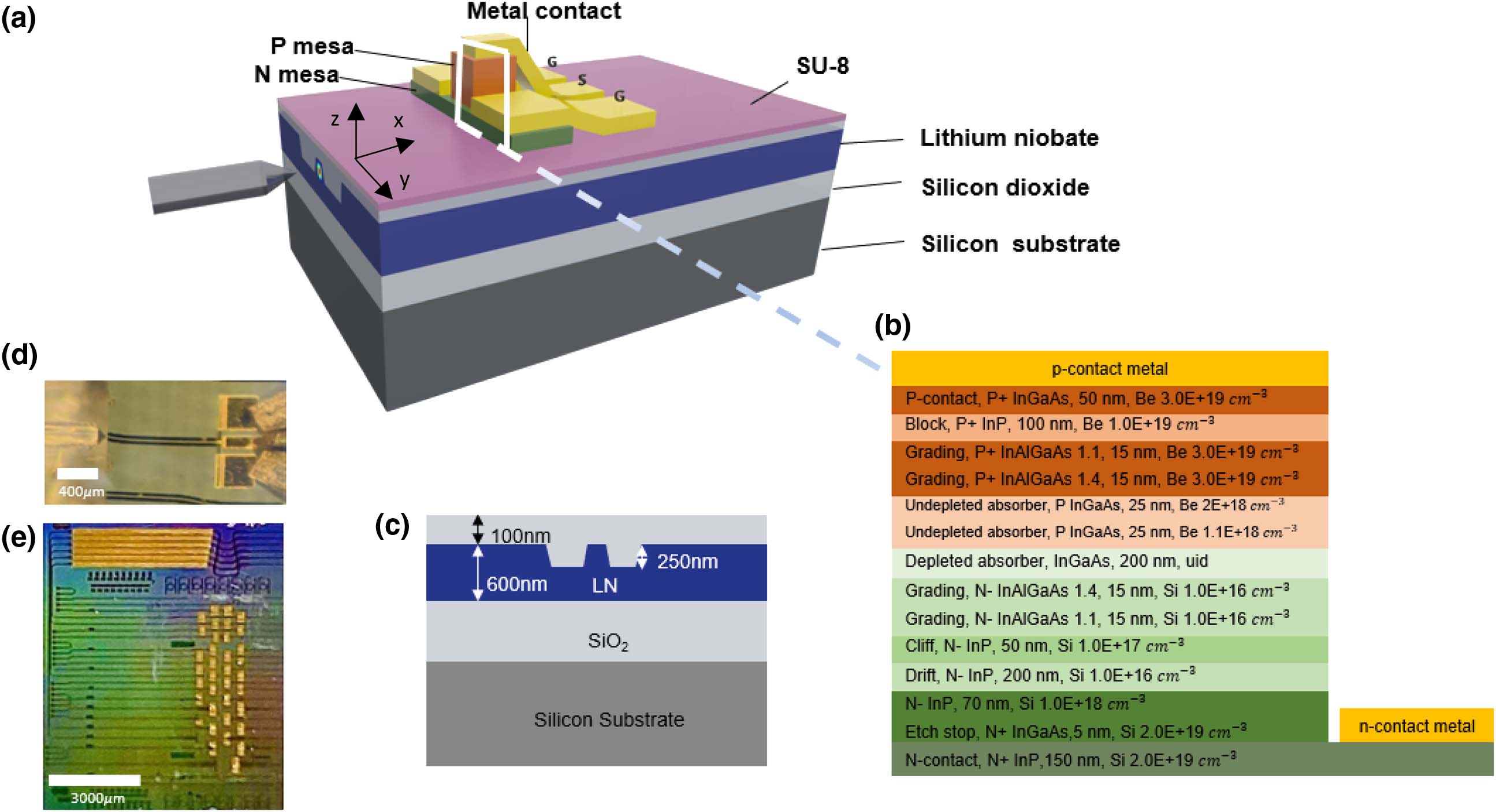
    Fig. 1. MUTC PDs integrated on TFLN. (a) Structural illustration. (b) Epitaxial structure of the n-down PD. (c) TFLN waveguide cross section. (d) Microscope image of a device under test with a lensed fiber and a radio frequency probe. (e) Microscope image of chip with integrated PDs.
    Device simulations. (a) Calculation of transit time-limited bandwidth versus undepleted absorber thickness with total absorber thickness of 250 nm and a fixed drift layer thickness of 200 nm. Optical simulations of E-field magnitude: (b) yz cross section at x=0 μm (passive waveguide), (c) yz cross section at x=5 μm (PD), and (d) zx cross section at y=0 μm.
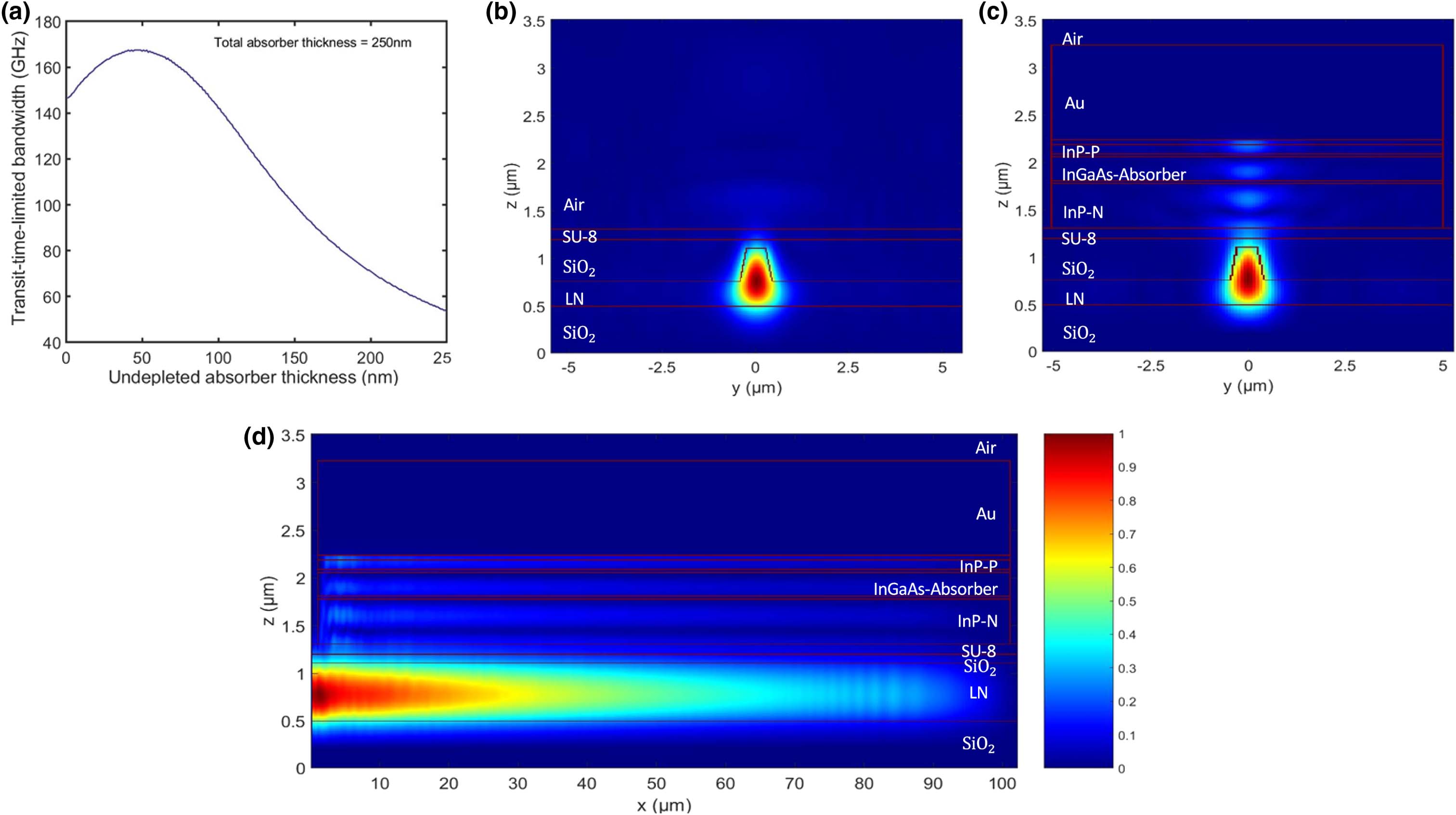
    Fig. 2. Device simulations. (a) Calculation of transit time-limited bandwidth versus undepleted absorber thickness with total absorber thickness of 250 nm and a fixed drift layer thickness of 200 nm. Optical simulations of E-field magnitude: (b) yz cross section at x=0  μm (passive waveguide), (c) yz cross section at x=5  μm (PD), and (d) zx cross section at y=0  μm.
    DC measurements of MUTC photodiodes integrated on thin-film LN platform. (a) Dark current characteristics of a 1400-μm2 device. (b) Measurement of photocurrent versus optical power (measured at fiber tip) of a 600-μm2 device.
    Fig. 3. DC measurements of MUTC photodiodes integrated on thin-film LN platform. (a) Dark current characteristics of a 1400-μm2 device. (b) Measurement of photocurrent versus optical power (measured at fiber tip) of a 600-μm2 device.
    AC measurements of MUTC photodiodes integrated on thin-film LN. (a) Frequency responses of a 100-μm2 PD at different photocurrents. (b) Frequency responses of various sized photodiodes at 1-mA photocurrent and 3-V reverse bias. (c) Simulations and measurements of bandwidth for different device areas. (d) Measurement of RF power of a 300-μm2 PD at 48 GHz at different reverse biases.
    Fig. 4. AC measurements of MUTC photodiodes integrated on thin-film LN. (a) Frequency responses of a 100-μm2 PD at different photocurrents. (b) Frequency responses of various sized photodiodes at 1-mA photocurrent and 3-V reverse bias. (c) Simulations and measurements of bandwidth for different device areas. (d) Measurement of RF power of a 300-μm2 PD at 48 GHz at different reverse biases.
    Eye diagram measurement. (a) Measurement system setup. (b) Measured eye diagram for a commercial photodiode. (c) Measured eye diagram for an MUTC photodiode on TFLN with 200-μm2 PD area.
    Fig. 5. Eye diagram measurement. (a) Measurement system setup. (b) Measured eye diagram for a commercial photodiode. (c) Measured eye diagram for an MUTC photodiode on TFLN with 200-μm2 PD area.
    Thermionic emission velocity in InGaAs2.5×105  m/s
    Hole saturation velocity0.45×105  m/s
    Electron velocity in InGaAs and InP1×105  m/s
    Electron mobility in p-type InGaAs0.5  m2/(Vs)
    Electron diffusivity in p-type InGaAs1.3×102  m2/s
    External load resistance50 Ω
    Series resistance5 Ω
    Table 1. Bandwidth Calculation Parameters
    Xiangwen Guo, Linbo Shao, Lingyan He, Kevin Luke, Jesse Morgan, Keye Sun, Junyi Gao, Ta-Ching Tzu, Yang Shen, Dekang Chen, Bingtian Guo, Fengxin Yu, Qianhuan Yu, Masoud Jafari, Marko Lončar, Mian Zhang, Andreas Beling. High-performance modified uni-traveling carrier photodiode integrated on a thin-film lithium niobate platform[J]. Photonics Research, 2022, 10(6): 1338
    Download Citation