• Acta Photonica Sinica
  • Vol. 50, Issue 6, 179 (2021)
Tuo WANG1、2, Hongmei CHEN2, Huimin JIA1, Zhonghui YAO2, Dan FANG1, Cheng JIANG2, Ziyang ZHANG2, Kexue LI1, Jilong TANG1, and Zhipeng WEI1
Author Affiliations
  • 1State Key Laboratory of Hight Power Seminconductor Laser, College of Science, Changchun University of Science and Technology, Changchun30022, China
  • 2Suzhou Institute of Nano-Tech and Nano-Bionics, Chinese Academy of Science, Suzhou, Jiangsu1513, China
  • show less
    DOI: 10.3788/gzxb20215006.0623002 Cite this Article
    Tuo WANG, Hongmei CHEN, Huimin JIA, Zhonghui YAO, Dan FANG, Cheng JIANG, Ziyang ZHANG, Kexue LI, Jilong TANG, Zhipeng WEI. Performance Research and Fabrication of 1 310 nm Superluminescent Diodes with High Power[J]. Acta Photonica Sinica, 2021, 50(6): 179 Copy Citation Text show less
    Schematic diagram
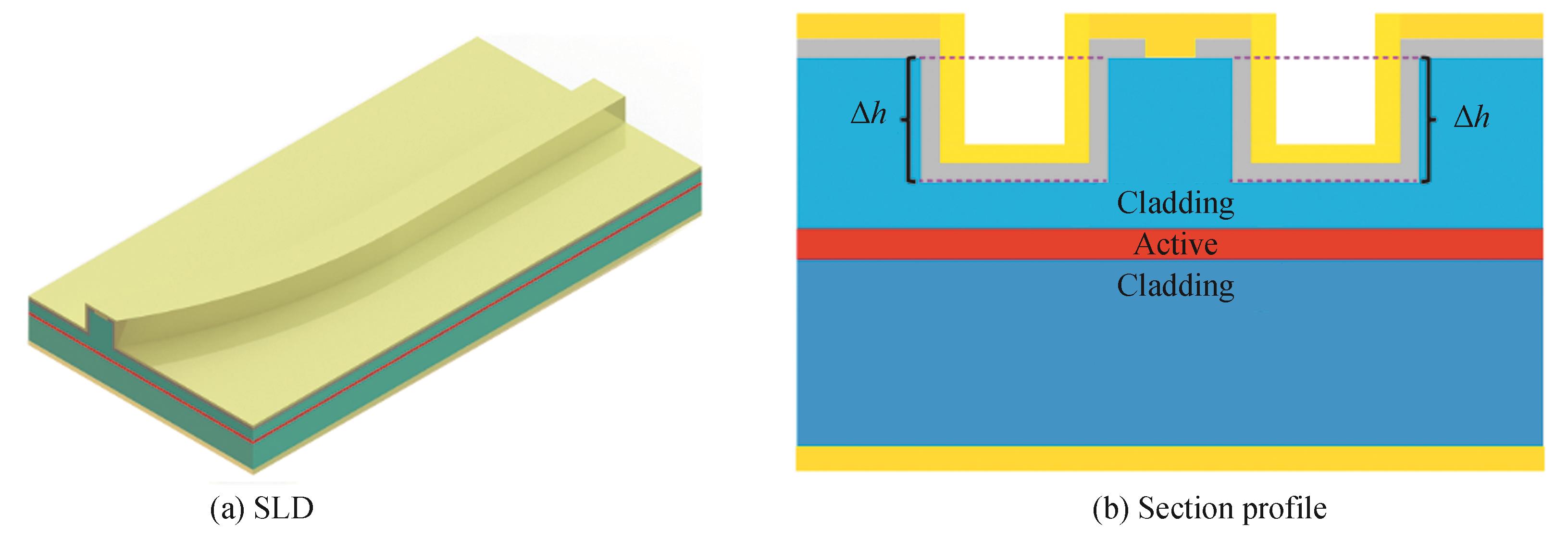
    Fig. 1. Schematic diagram
    Schematic diagram of ridge waveguide structure that is equivalent to three-layer planar waveguide model
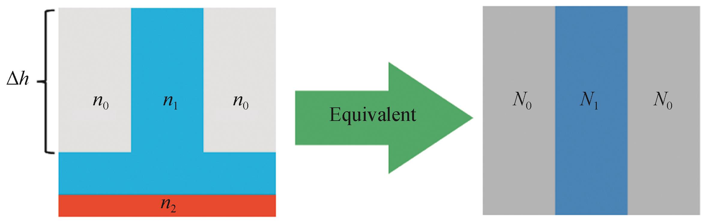
    Fig. 2. Schematic diagram of ridge waveguide structure that is equivalent to three-layer planar waveguide model
    The calculation of effective refractive index
    Fig. 3. The calculation of effective refractive index
    The simulation of the optical field on the device cavity surface with different etching depths
    Fig. 4. The simulation of the optical field on the device cavity surface with different etching depths
    The simulation of the optical field in waveguide with different etching depths
    Fig. 5. The simulation of the optical field in waveguide with different etching depths
    The simulation of the optical field in waveguide with different bending angles
    Fig. 6. The simulation of the optical field in waveguide with different bending angles
    The simulation of the thermal field of devices with different SiO2 thicknesses
    Fig. 7. The simulation of the thermal field of devices with different SiO2 thicknesses
    Microscope picture of the fabricated device
    Fig. 8. Microscope picture of the fabricated device
    The testing results of the devices
    Fig. 9. The testing results of the devices
    NameStraight waveguide length/mmMaximum injection current/mA

    Slope

    efficiency/(W·A-1

    Spectral width/nmOutputpower/mW
    SLD-12.51 0000.0587.636.5
    SLD-22.05000.06424.9
    SLD-31.55000.11042.2
    Table 1. The testing results of the device with 8° bending angle
    Tuo WANG, Hongmei CHEN, Huimin JIA, Zhonghui YAO, Dan FANG, Cheng JIANG, Ziyang ZHANG, Kexue LI, Jilong TANG, Zhipeng WEI. Performance Research and Fabrication of 1 310 nm Superluminescent Diodes with High Power[J]. Acta Photonica Sinica, 2021, 50(6): 179
    Download Citation