
Zheng Wang, Libing Zhou, Wenting Xie, Weiguang Chen, Jinyuan Su, Wenxuan Chen, Anhua Du, Shanliao Li, Minglan Liang, Yuejin Lin, Wei Zhao, Yanze Wu, Tianfu Sun, Wenqi Fang, Zhibin Yu. Accelerating hybrid and compact neural networks targeting perception and control domains with coarse-grained dataflow reconfiguration[J]. Journal of Semiconductors, 2020, 41(2): 022401
- Journal of Semiconductors
- Vol. 41, Issue 2, 022401 (2020)
Abstract
1. Introduction
Recent advancements in neural networks have demonstrated their success in a wide range of application domains, such as computer vision, natural language processing, and gaming engines. Although questions still exist on the appliance of neural networks into further domains, there is inarguably the increasing demand on the computing power to support fast-evolving network structures.
Traditionally, neural networks are mostly deployed on CPU and GPU-based platforms, resulting in either less computing performance or huge power consumption. Recently, the CPU-FPGA based heterogeneous programming paradigm has also appeared to support higher performance. However, both solutions suffer from extensive power consumption caused by a significant amount of data movement between computing elements. Dedicated hardware accelerators have been proposed to accelerate the inference phase of neural networks such as Eyeriss[
Standard convolution plays a key role in feature extraction, its amount of computation and network parameters have been increasing rapidly[
On the other hand, the AI community has also witnessed the applications of neural networks in non-perceptual domains such as decision-making. In the domain of control systems, decision making through deep reinforcement learning has shown progressive achievements. The deep Q network (DQN), which was originally proposed in Ref. [13], uses multi-layer neural networks to implement the Q-function in order to eliminate the lookup-table for storing Q-values. Deepmind demonstrates a ground-breaking contribution in Ref. [14] by combining CNN and DQN to realize beyond human-level performance in Atari gaming. AlphaGo[
Consequently, there is a high probability that future neural networks are capable of performing end-to-end tasks in perception, control, and even actuation with hybrid, compact algorithmic kernels. However, current dataflow techniques such as weight-stationary (WS), output-stationary (OS) and row-stationary (RS)[
2. Data flow for neural network kernels
2.1. Standard kernels
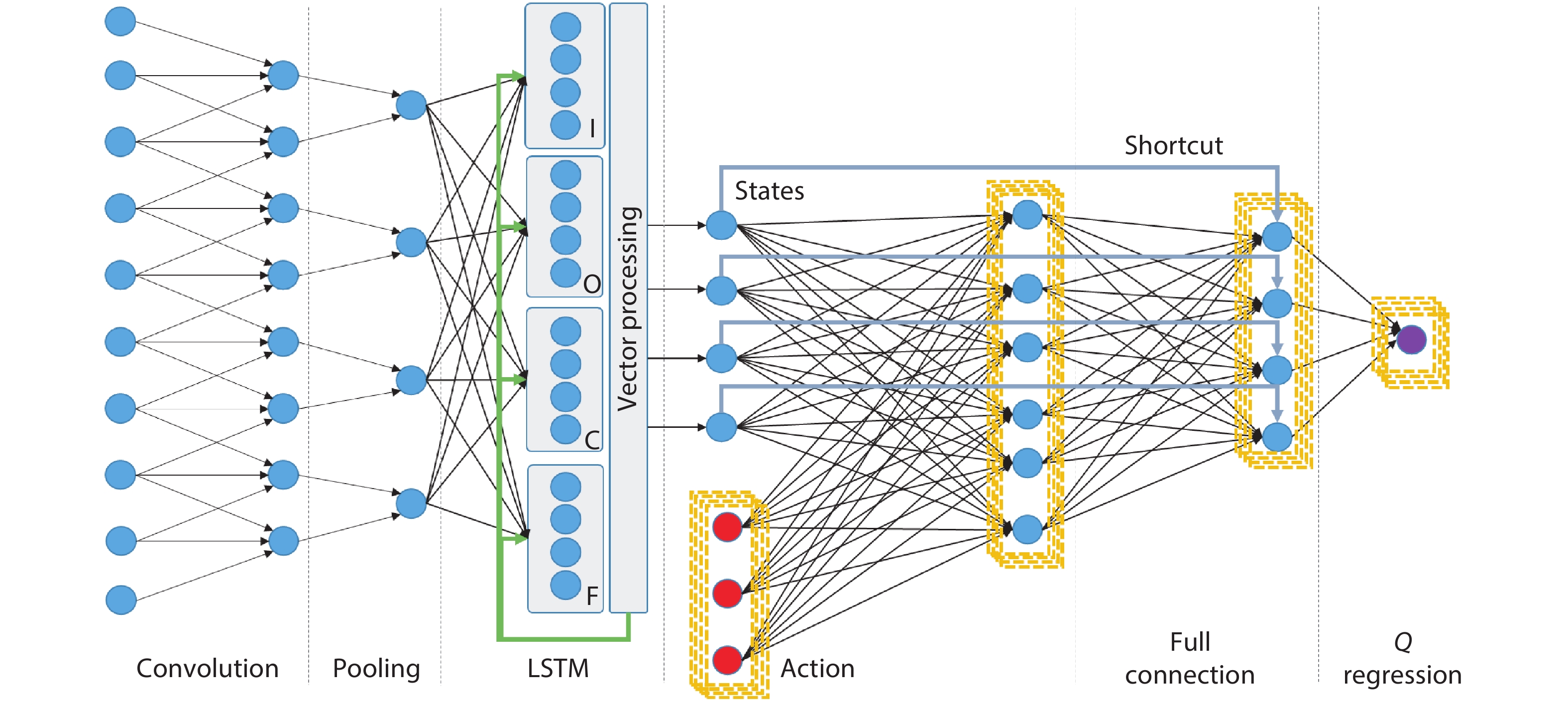
Fig. 1 visualizes important network layers and their interconnections, which form an end-to-end network targeting both perception and control. Especially for graphical input, concatenated convolution and pooling layers are applied as perceptional building blocks for extracting visual features. Model networks such as Yolo-v3 and Resnet-50 can have tens of such layers, imitating the human visual system. For timing sequence-dependent applications, such as video context understanding and language processing, sequences of extracted features through time are provided as input to the LSTM layer, which extracts sequence-dependent features. Opposed to former layers, LSTM constitutes four basic gates, naming input (I), output (O), cell state (C) and forget (F) gates. While I, O and F gates compute layer output through vector operations, C gate keeps the current layer states which are also provided as recurrent input for the next sequence in time.
![]()
Figure 1.(Color online) Structure of hybrid neural network targeting perception and control with layer-wise algorithmic kernels.
The control network starts after feature extraction layers. In DQN, the extracted features are treated as nodes of states, while the optimal decision needs to be chosen through nodes of actions. The approach is to iterate through all possible actions under current states and perform regression to find maximal or minimal output value (Q value) depending on strategies of reinforcement learning. The procedure is represented as a state-action layer in Fig. 1. Since action nodes need to be iterated, all computation in the following layers needs to be iterated as well, represented as yellow dash boxes. The fully connected layer is prevalent since the invention of the multi-layer perceptron. However, shortcut links are often used, especially in residue networks, to improve the accuracy of classification and regression by providing features form layers before the current input.
Various layers differ not only in the network structures, but also operands, operators, nonlinear functions. Table 1 summarizes the characteristics of multiple kernel layers. It is observed that pooling and shortcut operate on vectors while other kernels operate on matrix, among which convolution processes sparse matrix and the rest kernels process dense matrix. Concerning nonlinear functions, LSTM adopts simultaneously sigmoid and tangent while the rest matrix kernel uses either ReLU or sigmoid.
The dataflow properties are generalized from network structure. In convolution and fully connected layers, activations (network data) need to be shared among nodes of the output feature map. LSTM adopts similar serial streaming with the special case that activation streams need to be shared among multiple gates. The state-action layer, on the other hand, requires fast data flow generation based on the iteration of action nodes. Pooling and shortcut which operate on vectors do not need to share activation for feature maps. Therefore vector types of activation can be streamed in parallel.
Furthermore, we analyze the functionality of the intermediate data used in multiple kernels. Due to the nature of data sparsity, convolution and pooling are dominant by activations, while on the contrary, FC and LSTM are dominant by weights. LSTM and State-action contain generated data for cell states and actions, respectively. In the shortcut layer, pointers to activations of the previous layer need to be bookkept, for the network to address previous data.
2.2. Compact convolutions
The essences of compact CNNs are depthwise (DW) and pointwise (PW) convolution. As shown in Fig. 2, DW convolution utilizes a unique 2-D filter to convolve data within a single input channel. PW convolution, on the other hand, applies a 1-D filter to perform linear combination across multiple channels. We label the dimension of input feature map (Ifmap) by DF × DF × M where DF is the spatial height and width, M is the number of input channels. The output feature map (Ofmap) after DW convolution has the dimension of DF × DF × M, which is passed onto PW convolution as Ifmap. The Ofmap of PW convolution is DF × DF × N. The number of operations compared to standard convolution is present in Table 2, which is evaluated in the number of multiply-and-accumulation (MAC). For the typical DK value of three, replacing standard convolution with DW and PW convolution leads to MAC reduction up to 90%[
![]()
Figure 2.Orientation and dimensions of compact CNN filters.
Table Infomation Is Not EnableFig. 3 visualizes the MobileNet structure, which concatenates several network layers. Besides standard convolution, pooling, FC and softmax layers that are available in conventional CNN, thirteen repeated blocks of DW and PW convolution play a crucial role in network organization. As shown in the statistics chart, 94.85% of total operations in MobileNet is PW convolution while DW convolution ranks the second by 3.06%. Other compact CNNs follow similar statistics of operations, which indicates massive demand in the acceleration of PW and DW convolution.
![]()
Figure 3.(Color online) Structure and operation distribution for Mobile-Net.
3. Reconfigurable dataflow processor
According to the analysis of algorithmic kernels on Section 2, a dataflow processor is designed to achieve dynamic functional reconfiguration through coarse-grained dataflow management. This section describes the design methodology, micro-architecture, instruction set architecture, and associated toolchain for model conversion from mainstream deep learning frameworks.
3.1. Methodology of dataflow reconfiguration
To implement standard algorithmic kernels in Table 1 and possibly save hardware resources, the design of reconfigurable architecture should at least cover the union of different kernels. To achieve this, the resources are maximally shared among kernels, including PEs, data input/outputs, buffering SRAMs and DRAM interfaces. Fig. 4 illustrates the methodology of data flow management and resource sharing, which is also explained as the following:
![]()
Figure 4.(Color online) Reconfiguration of dataflow, PE and storage functionalities for standard kernels.
Convolution: PEs, which are configured as MAC and ReLU in function, are grouped in multiple threads, where each thread processes data with the same row and column across multiple channels of the output feature map. SRAMs are mostly used for buffering thread dependent activations of the input feature map. Weights are shared across multiple threads. Activations are serially streamed from the individual buffer to achieve sharing among PEs. Serial outputs from individual threads are associated in the output buffer and streamed out in parallel through SERDES and DRAM controller.
Pooling: PEs are configured as a comparator to achieve max and min operators. Since pooling operates on vectors, the activations fetched from DRAM are directly provided to PE arrays without buffering, which extensively saves dynamic power consumption. Both parallel input and output are utilized. Activations are compared through time by modifying DRAM access addresses.
Full connection: for such weights dominant kernel, SRAMs are configured as weight buffers while activations are serially streamed through multiple threads. Outputs and PE configurations are similar to convolution.
Shortcut: Similar to pooling, the kernel works on vectors. The PEs are configured as an addition. Since two vectors are added, both input and output shift registers are used to store operands, which results are written to the output shift registers and written to DRAM in parallel. The pointer buffer is instantiated to address both operands in DRAM.
LSTM: PEs are grouped into four sets of gates which each set instantiates different nonlinear functions between sigmoid and tangent. Additional vector operators and tangent modules are used for post-processing. A mixed-mode input style is adopted for both activation sharing within each set of gates and fast data provision among different sets. Cell state buffer is instantiated to keep intermediate state information.
State-action: input/outputs and PE configurations are similar to full connection. Multiple origins of activations exist, including DRAM for conventional activations, on-chip buffering for activations of states and iterative actions.
Fig. 5 illustrates the proposed flow of data streaming for compact convolutions. Activations are associated into bundles. Each bundle has the size of a single read transfer of DRAM memory, which is eight bytes here for instance. Activations in the bundle are executed in parallel on multiple hardware threads. For PW convolution, bundle groups horizontal data elements. Burst read mode of DRAM streams eight input threads of data bundles vertically and simultaneously computes eight output threads. Showing in Fig. 5, with only four streams the Ofmap with the size of 16 × 16 is ready to commit. On the contrary, for DW convolution, bundle vertically groups eight data elements and streams horizontally. After streaming multiple rows of Ifmap depending on the filter dimension, bundles of multiple data in Ofmap are ready to commit. The grouping and streaming directions are in orthogonal to the filter dimension, which maximally exploits computing parallelism.
![]()
Figure 5.(Color online) Reconfiguration of dataflow for pointwise (PW) and depthwise (DW) convolution kernels.
The alternating direction of streaming and committing is designed to cater to the nature of alternating PW and DW layers in compact CNN. Therefore, no extra logic and cycles are required to re-arrange data alignment, which achieves a high saving in execution time and hardware cost.
3.2. Microarchitecture
The microarchitecture of the proposed reconfigurable dataflow processor is illustrated in Fig. 6. It employs a hierarchical design methodology, including PE, hardware thread and system-on-chip. This subsection introduces the individual module and its design considerations.
![]()
Figure 6.(Color online) Microarchitecture of proposed reconfigurable dataflow processor.
System-on-chip: this abstraction performs system-level coordination of individual threads and PEs. It is composed of four subsystems: execution controller, direct memory access (DMA) controller, execution threads, and buffers.
The execution controller mainly coordinates PEs and buffers according to network instructions. Upon initialization, it fetches instructions from DRAM into configuration SRAM, sequentially decodes each instruction and drives execution threads to achieve targeting network functions. A centralized control methodology is adopted to reduce logic overheads and boost performance.
The DMA controller achieves multiple modes of reads and writes between SoC and external DRAM storage. It fluently transmits network configurations, weights, activations, and results. DDR burst mode is considerably adopted to rapidly provide data and reduce DRAM access power. It is well-known that memory bandwidth incurs limitation to the computational throughput. Hence, we design the DMA according to the algorithmic properties, specified in Section 3. For instance, the data bundle for PW and DW convolution has the size of elements equaling to the number of bytes per transfer under a specific DRAM protocol. Therefore continuously burst read and write are possible without further data buffering.
A pool of SRAM buffers is designed where each SRAM has 8 KB size. The analysis in Section 3 inspires the SRAM pool structure, where different algorithmic kernels have divergent usage of buffering. With the assistance of the execution controller, the SRAM is instantiated into various buffering functions on the fly, determined by algorithmic kernels. For detailed usage of the SRAM pool, please refer to buffering properties in Table 1.
Hardware threads: this design abstraction is introduced for easy management of resource sharing for both data flow and weights. Activation inputs and outputs are built using shift registers to achieve both data sharing and fewer power overheads due to single fan-out and reduced load capacitances. Shift registers can be dynamically configured as serial and parallel modes according to Fig. 4. In contrast to the single direction of the in-data stream, the out-data stream is bidirectional to facilitate vector computation used in shortcut kernel. Multiple PEs are coordinated through thread-level finite state machine (FSM) to process activations and weights in a pipeline fashion. The weights are streamed-in from the SRAM pool in the SoC, where individual PEs can receive different weight streams.
Processing elements: To efficiently compute kernel-dependent functions, PE is compactly designed to achieve required operators. It facilitates both matrix and vector computation through both data input ports and one weight input port. The Sigmoid and Tangent modules are designed based on the linear approximation technique in Ref. [19]. The control input receives opcode from thread-level FSM to configure multiplexers to realize kernel-dependent operators.
3.3. Instruction set and toolchain
Customized instruction set architecture for the proposed processor is designed, supporting neural network algorithmic kernels in Section 3. As shown in Fig. 7, instructions have a length of 96 bits and contain divergent fields across instruction types. In general, the proposed ISA specifies the operator (opcode in first five bits), properties of input and output operands, quantization bit for activation and weight addressing index from DRAM. Address for activation is not necessary for the majority of layers since the following layer reads activations from the previous layer by default.
![]()
Figure 7.(Color online) Instruction set architecture (ISA) and developing toolchain.
For convolution and pooling, dimension descriptions on Ifmap, Ofmap, and filters are specified, as well as stride and padding properties. Convolution modes of standard, PW and DW are automatically decoded in micro-architecture according to filter dimensions. Pooling instruction contains the strategy field for choosing between max, min, and average pooling.
The nonlinear function layer can be specified among ReLU, sigmoid, tangent, and bypass. The state-action layer contains an extra field for size of action nodes, strategy selection, plus the probability of random action taking (epsilon greedy) and associated random number seed. The details of DQN architecture and controlling strategy is referred to Ref. [20].
The shortcut layer operates on two vector operands; hence, their activation addressing (pointer) and sizes need to be specified in the instructions. LSTM layer contains fields of sequence-dependent cell state nodes besides regular input nodes.
The design methodology of the proposed architecture favors an ASIC design manner instead of a CPU centric one. Typically ASIC adopts a finite state machine for control flow instead of RISC-style instructions in the CPU. The instruction or configuration in ASIC tends to guide the state transition from higher abstraction, to realize the design of multi-mode functional circuits. Consequently, the customized layer-wise instructions facilitate data stream reconfiguration according to Figs. 4 and 5. Compared to traditional RISC style ISA, such high-level ISA constructs the abstraction layer which leaves fine-grained operation management to the controller state machine in the processor and significantly simplifies the compilation flow of neural networks.
The developing tool flow converts the state-of-the-art network model to deployable format on proposed architecture. Taking Keras network h5 model[
3.4. Operation management
The internal finite state machine contains more than 100 states for activation/weight buffering, synchronization of multiple threads and processing with high utilization of PEs. For brevity, the FSM is not explicitly described in this section. Instead, phases of operations are summarized below and also presented in Fig. 8.
![]()
Figure 8.(Color online) Operational phases of proposed architecture.
Initialization phases: Such phases load network instructions, weights and input activation from the host machine to DRAM of the processor with specific locations for all three types of data. The interface with the host can be one of the SERDES such as PCI-e. Afterwards, the instructions are loaded from DRAM to CFG buffer in the SoC. Currently an 8 kB size of CFG buffer is deployed to hold a maximum of 682 layer network instructions, which is sufficient for mainstream artificial neural networks.
Computation phases: The SoC controller fetches, decodes each network instruction and reconfigures the dataflow according to Figs. 4 and 5. The duration of reconfiguration takes only eight clock cycles including fetch and decode. Subsequently, weights for corresponding network layer and input activations are streamed into individual threads and processed by PEs. Weights and activations are streamed with an interleaved manner to maximally exploit the length of burst access of DRAM. Once upon completion of the network layer, the controller iterates onto the next layer and continues reconfiguration and data streaming. Intermediate results are streamed to and from DRAM without external manipulation.
Output phases: When the last network layer is complete, the controller streams multiple batches of results to DRAM. Once all results are available, they are streamed from DRAM to host through SERDES. The next batch of input activations is ready to be streamed-in after the output of the current result.
4. Experiments
4.1. Design methodology
The demonstrated architecture with 108 kB on-chip SRAMs and 16 PEs fitting in one single thread is designed completely in Verilog and simulated using Modelsim to characterize performance on individual network kernels. Logic synthesis by Design Compiler is carried out under UMC CMOS 65 nm low-leakage technology library. Placement and routing are performed by Innovus to generate layout. Calibre is for physical verification and sign-off. The prototype chip has been fabricated by UMC through a multi-project wafer (MPW) service provided by Europractice.
Currently, IPs for DRAM and PCI-e interfaces are missing in the taped-out chip. To verify the designed DMA controller and DRAM data access, simulation models of 512 MB DDR3 DRAM, memory controller and PHY (MIG) are generated using Xilinx ISE with a DQ width of 16 bits and DDR frequency of 800 MHz. Opal Kelly Frontpanel technology[
The exemplary design on FPGA contains 256 PEs fitting in 16 hardware thread, 18 × 6 kB on-chip SRAM buffers, including 16 reconfigurable SRAM blocks, one configuration SRAM and one special purpose SRAM. The dimensions of PEs and SRAMs are chosen to match the data width provided by the DRAM for better utilization of off-chip memory bandwidth.
Toolchains for network model conversion is developed in Python. Currently, the Tensorflow Keras h5 model is supported, while integration with Caffee and Darknet frameworks are under development. After DRAM calibration, converted network configuration, inputs, and weights are downloaded into specific address spaces in DRAM through Frontpanel and DMA controller in the SoC. Upon completion of model downloading, the SoC begins layer-wise processing according to reconfigurable dataflow described in Section 3. Benchmarks are chosen from Keras framework in Python and neural network toolboxes in MATLAB.
4.2. Performance analysis
Three network structures have been demonstrated to analyze the performance of the proposed architecture: First, MobileNet with hybrid kernels of standard, PW and DW convolutions, pooling and full connection. Second, maze walkthrough by DQN with state-action and full connection kernels. Third, sequence classification with hybrid kernels of LSTM and full connection.
MobileNet: As introduced in Section 2.2, MobileNet adopts iteratively compact convolution kernels, which account for 97.91% of computation in the number of MACs. Table 3 shows the profiled execution latency of proposed design throughout various layers of MobileNet, benchmarked between multi- and single-threaded architecture, using an FPGA prototype with 256 PEs and DRAM support.
The total network latency with multi-threading is only 7.6% of the single-threaded design proposed in Ref. [22] under the same frequency of 100 MHz. Such acceleration is mainly due to the following factors. In DW convolution, maximal utilization of DRAM bandwidth and processing elements do not reach a high level. However, the 2-D filters across multiple channels are fetched from DRAM in a burst manner and computed with data elements of a bundle in parallel, which consequently leads to a 21.9× saving of latency. On the other hand, PW convolution achieves a 16× speed-up due to maximal 100% usage of memory bandwidth and PEs, which is only possible with the assist of continuously addressed data bundles in burst mode.
Besides compact convolution layers, the first layer of standard convolution is processed only in the single thread due to the irregular addressing for three channel RBG feature maps, which incurs only 6.7% of PE utilization. Ongoing work is targeting the issue of irregular addressing with multi-functional on-chip SRAMs. The pooling layer is executed with parallel input and output stream on a single thread as shown in Fig. 4(b). A fully connected kernel utilizes 16 PEs similar to a single-thread design. The parallelism is limited by the fact that the weight stream for individual output node in the FC layer cannot be shared among PEs and noted that the processing latency considers not only streaming of activation but also weights, which accounts for ~60% of latency for full connection.
Deep reinforcement learning: a typical usage of DQN is maze walking, where the intelligent agent learns to walk towards the destination by picking right directions at the crossroad and also avoiding barriers. To model maze walking with the state-action layer in DQN, the actions for the agent upon choices are modeled as discrete action nodes, where states are modeled with whether the agent's faces surrounded barriers in different directions. For details on modeling maze walking with DQN, the readers are referred to Ref. [26].
After modeling, we tune the sizes of state and action space and compare the computation time consumed by different structures of the DQN network and the dimensions of the action space. As shown in Fig. 9, one, two, four and six nodes of action space are tested on the 2-, 5-, and 10-layer network, while state space is chosen between 128 and 256 nodes. For all tested action space, the on-chip Q iterative time of all three network structures is less than 2 ms. Such iteration time slightly increases with the dimension of action space as well as the network size.
![]()
Figure 9.(Color online) Comparison of
We profile the Q iteration time for the same configuration of network and action space on the host machine with the Intel i7 processor. MATLAB with Neural Network Toolbox with the feature of runtime profiling is used for benchmarking. As shown in Fig. 5, the proposed architecture with on-chip Q iteration achieves at least 100 × speed-up compared to the host machine for all configurations, demonstrating the advantage of the proposed architecture for decision network.
Sequence classification: the testing example employs sensor data obtained from smartphone worn on the body[
Table 4 presents the testing network with layer-wise structure specifications. Performance is benchmarked on the following three platforms: Intel i7 CPU and NVIDIA GTX GPU with measured latency in MATLAB neural network toolbox and proposed design of 16 PEs with simulated latency in Modelsim. It is observed that for all network specifications, the proposed design achieves improved performance compared to CPU and GPU. It is noticed that the measurement results from MATLAB consider huge latency of data transfer between disk, main memory, and operating system, whereas our design is proposed as a standalone system. However, future LSTM networks tend to be deployed on sensors and process data directly from DRAM, which is close to the design principle of our design. CPU and GPU consume three orders of magnitudes higher power than the proposed design, proving the energy efficiency of ASIC for hybrid neural networks.
4.3. Physical results
The reconfigurable ASIC has been taped-out with UMC CMOS 65 nm low-leakage technology. Fig. 10 presents the chip’s layout and micrograph. The ASIC has a die size of 1.8 × 1.8 mm2 including 80 IO pads, 16 PEs, and 18 SRAM blocks. The driving voltage for the core and IO is 1.2 and 2.5 V respectively. The chip communicates with testing FPGA board using customized 8-bit input and output data ports.
![]()
Figure 10.(Color online) (a) ASIC layout with 16 reconfigurable PEs. Logics (middle) surrounded by 18 SRAM blocks. (b) Micrograph of taped-out chip with UMC CMOS 65 nm low-leakage technology.
Regarding the layout, SRAM IPs with 6 kB each occupy ~50% of the core’s die area. The size of SRAM IP is chosen to fit the number of weights per channel of typical convolution Ofmap (Up to 3 × 3 × 512 filter dimension). Orientations of SRAMs are carefully adjusted so that controlling logic and PEs can be placed in the middle area, with reduced routing overhead. The current ASIC only contains 16 PEs. However, the vast die area with fillers (blue) suggests that a huge amount of extra PEs can be placed on the die, which should efficiently share the pool of SRAMs with the design methodologies introduced in Section 3. Estimates through Innovus imply an average power consumption of 55.4 mW on the die of 256 PEs and the same 18 SRAMs, which boosts the energy efficiency to 0.92 TOPs/W with further improvement possibilities.
From a functional perspective, the ASIC supports reconfiguration between standard convolution, max/min pooling, and full connection. Layer-wise kernel type, activation and filter dimension, nonlinear functions can also be reconfigured using ISA in Section 3.3.
As shown in Fig. 11, the testing board has been designed to integrate the socket of the CLCC84 chip package and FPGA interfacing with a host machine from Ref. [24]. The testing infrastructure is demonstrated in Fig. 12, where Python APIs are used to transmit/receive signals, and oscilloscopes are equipped for measuring signal voltages and core currents.
![]()
Figure 11.(Color online) Views of the testing board. The front view contains testing IC under CLCC84 packaging and socket. The rear view contains FPGA for interfacing IC with the host machine.
![]()
Figure 12.(Color online) Testing infrastructure with measurement of both signal voltages and currents.
Regarding runtime power consumption, we measure the core current by deploying five layer neural networks, as shown in Fig. 13. It is observed that two convolutional layers incur long execution time and large current. Pooling layers have a relatively shorter time and smaller current, while the FC layer has high power but a very short running time. Both initialization and idle phases consume similar currents. Table 5 shows the statistics of average power consumption for each operating phase under different running frequencies. At the design frequency of 100 MHz, the largest power value 8.97 mW is consumed by the FC layer, while the average power throughout operating phases of neural networks (form Conv1 to FC) is 7.51 mW, which implies the energy efficiency of 426 GOPs/W.
![]()
Figure 13.(Color online) Runtime current measurement across different phases of operation under 30 MHz frequency.
Table 6 shows a comparison between our work and other state-of-the-art works. Our taped-out IC with 16 PEs achieves the minimal measured power 7.51 mW among other designs, which is highly customized to ultra-low power applications. In contrast, the multi-threaded version with 256 PEs has the estimated energy efficiency of 0.92 TOPS/W, which is comparable to the state-of-the-art designs.
5. Conclusion
Neural networks have demonstrated tremendous success in a wide range of application domains, which drives research on specific AI accelerators in the past five years. Majority of customized AI accelerators targets convolutional neural network, while hybrid networks with non-standard layers have been purposed for applications beyond vision-based perception. In this work, we purpose a reconfigurable dataflow processor targeting multiple algorithmic kernels for both perception and control. Using the supported kernels, not only standard CNN but also compact CNN, ResNet, LSTM and deep reinforcement learning algorithms can be constructed.
The architecture is designed with a separate pool of PEs and SRAMs, whose functionalities are instantiated based on layer description through custom-designed ISA. Toolchains have been built to achieve compatibility with state-of-the-art AI programming framework. Experiments on profiling for three types of neural networks demonstrate the performance, resource utilization and special design features against the Intel processor. The taped-out ASIC under 65 nm UMC CMOS technology with 16 reconfigurable PEs is also demonstrated.
Future work includes optimization techniques regarding resource utilization, power consumption, reliability based on the design methodology. Further techniques to maximize resource sharing with low controlling overhead is the key to the enhancement of energy efficiency.
Acknowledgments
This work was supported by NSFC with Grant No. 61702493, 51707191, Science and Technology Planning Project of Guangdong Province with Grant No. 2018B030338001, Shenzhen S&T Funding with Grant No. KQJSCX20170731163915914, Basic Research Program No. JCYJ20170818164527303, JCYJ20180507182619669, and SIAT Innovation Program for Excellent Young Researchers with Grant No. 2017001.
References
[1] Y Chen, T Krishna, J Emer et al. Eyeriss: An energy-efficient reconfigurable accelerator for deep convolutional neural networks. IEEE J Solid-State Circuits, 52, 127(2017).
[2]
[3]
[4] J Cong, B Xiao. Minimizing computation in convolutional neural networks. Artificial Neural Networks and Machine Learning, 281(2014).
[5] S Yin, P Ouyang, S Tang et al. A high energy efficient reconfigurable hybrid neural network processor for deep learning applications. IEEE J Solid-State Circuits, 53, 968(2017).
[6] O Russakovsky, J Deng, H Su et al. ImageNet large scale visual recognition challenge. Int J Comput Vision, 115, 211(2015).
[7]
[8]
[9] K Simonyan, A Zisserman. Very deep convolutional networks for large-scale image recognition. arXiv preprint arXiv:1409.1556, 2014.
[10]
[11]
[12]
[13] V Mnih, K Kavukcuoglu, D Silver et al. Playing atari with deep reinforcement learning. arXiv: 1312.5602(2013).
[14] V Mnih, K Kavukcuoglu, D Silver et al. Human-level control through deep reinforcement learning. Nature, 518, 529(2015).
[15] D Silver, A Huang, C Maddison et al. Mastering the game of Go with deep neural networks and tree search. Nature, 529, 484(2016).
[16] D Silver, J Schrittwieser, K Simonyan et al. Mastering the game of Go without human knowledge. Nature, 550, 354(2017).
[17]
[18] F Gers, J Schmidhuber, F Cummins. Learning to forget: Continual prediction with LSTM. 9th International Conference on Artificial Neural Networks, 850(1999).
[19]
[20]
[21]
[22]
[23]
[24]
[25]
[26]
[27]
[28]
[29]
[30] S Yin, P Ouyang, S Tang et al. 1.06-to-5.09 TOPS/W reconfigurable hybrid-neural-network processor for deep learning applications. Symposium on VLSI Circuits(2017).


Set citation alerts for the article
Please enter your email address

© Copyright 2018-2021 | Chinese Laser Press. All Rights Reserved 沪ICP备15018463号-20