Abstract
In this paper, we have shown that perfect absorption at terahertz frequencies can be achieved by using a composite structure where graphene is coated on one-dimensional photonic crystal (1DPC) separated by a dielectric. Due to the excitation of optical Tamm states (OTSs) at the interface between the graphene and 1DPC, a strong absorption phenomenon occurs induced by the coupling of the incident light and OTSs. Although the perfect absorption produced by a metal–distributed Bragg reflector structure has been researched extensively, it is generally at a fixed frequency and not tunable. Here, we show that the perfect absorption at terahertz frequency not only can be tuned to different frequencies but also exhibits a high absorption over a wide angle range. In addition, the absorption of the proposed structure is insensitive to the polarization, and multichannel absorption can be realized by controlling the thickness of the top layer.1. INTRODUCTION
In the past few years, the terahertz (THz) band has received increasing attention from researchers due to the significant progress of THz wave source research [1]. Applications of THz technology have been found in many different fields, such as information and communications technology, biomedical imaging, and nondestructive evaluation and security [1,2]. Under these circumstances, THz absorbers have also been greatly developed; they are widely used in solar photovoltaic cells, optical switches, optical detectors, filters, and biological and chemical sensors [3,4]. Therefore, the realization of perfect absorption at the THz band in different kinds of structures has received extensive attention in recent years. For instance, Xiang et al. presented a graphene-based hyperbolic metamaterial as the absorbing thin film to realize the critical coupling phenomenon [5]. Diem et al. demonstrated a wide-angle perfect absorber/thermal emitter in the THz regime using an array of tungsten wires on top of a silicon nitride substrate [6]. Wu et al. proposed broadband THz absorption enabled by coating an ultrathin antireflection film on a doped semiconductor considering coherent absorption [7]. Zhou et al. investigated a THz plasmonics perfect absorber whose absorption peak is independent of the incident angle based on a Fabry–Perot cavity [8]. Landy et al. studied a polarization-insensitive metamaterial absorber for THz frequencies [9]. Though sundry structures have been proposed to achieve tunable, broadband, and wide-angle perfect absorption, which can be applied in the field of solar power harvesting [10] and electromagnetic wave spatial filters [11], it is hard to implement these predominant properties in one structure or even realize a multichannel absorber. For this reason, creating a tunable and multichannel THz perfect absorber has attracted the attention of researchers, and is achieved by the Tamm surface plasmons with graphene in the present paper.
The Tamm surface plasmon, which is a new kind of surface wave confined at the interface between two different media, has attracted particular attention because of its potential applications in narrow-bandwidth multichannel absorbers and thermal emission devices [12,13]. Compared with traditional surface waves such as surface plasmon polaritons, optical Tamm states (OTSs) can be excited directly for both TE- and TM-polarized waves and it does not need a specific incident angle [14]. Due to these favorable conditions of OTSs, a large number of OTSs-based absorption devices have been put forward. Chen et al. reported a wide-angle perfect absorber based on OTSs with a metal–distributed Bragg reflector (DBR) construction [15]. Lu et al. researched the dual-channel absorption properties of OTSs in a metal–DBR–metal structure [16]. Fang et al. proposed a unidirectional all-optical absorption switch based on the theory of OTSs in a metal–DBR–metal plasmonic waveguide [17]. Up to now, most of the research on perfect absorption based on OTSs has been on wide-angle and narrowband absorption.
However, it is desirable to tune perfect absorption using external bias voltage or the nature of the material and implement three-channel (or higher) absorption. For this purpose, on one hand, a top layer can be placed between the graphene and one-dimensional photonic crystal (1DPC) to tune perfect absorption at different frequencies. On the other hand, introducing graphene into the perfect absorber also seems to be a good approach for controlling perfect absorption. Graphene, a two-dimensional carbon material that is one atom thick, has attracted intensive interest due to its unique optical and electrical properties [18,19]. It is a zero-bandgap material whose electromagnetic response can be realized from the UV to the THz range and is attractive for the possibility of controlling its carrier concentration via external gate voltages or chemical doping [20]. This means graphene’s conductivity can be continuously tuned over a broad frequency range by shifting the Fermi energy. It is even more important that graphene is intrinsically a semimetal and has some metallic properties under certain conditions [21,22]; this means that the graphene–1DPC composite configuration may excite OTSs. Grande et al. investigated a graphene-based absorber exploiting guided mode resonances in one-dimensional gratings [23]. It is attractive to investigate perfect absorption based on a graphene–1DPC structure.
Sign up for Photonics Research TOC. Get the latest issue of Photonics Research delivered right to you!Sign up now
In this paper, we present an effective method for achieving perfect absorption at the THz band by using a graphene–1DPC system. We show that we are able to control perfect absorption at different frequencies not only by changing the Fermi energy of graphene but also by adjusting the thickness and dielectric constant of the top layer. Moreover, we can achieve multichannel absorption by regulating the thickness of the top layer. At the same time, we can guarantee more than 90% absorption while the incident light is varied from 0° to 40°. Finally, we prove that perfect absorption can also be achieved with the loss and dispersion of the materials considered. We believe such work has potential applications in notch filters, solar cells, and directional absorbers for highly sensitive target identification of biological and chemical agents.
2. THEORETICAL MODEL AND METHOD
As is well known, an OTSs exists in the photonic crystal heterojunction and the metal–DBR structure [24,25]. Due to the metallic properties of graphene under certain conditions, here we propose a composite structure consisting of graphene and 1DPC, as shown in Fig. 1(a). The top layer is sandwiched between graphene and 1DPC, and the thickness is . The lower part of the top layer is followed by a 1DPC consisting of 20 cycles of DBR. The DBR is composed of two kinds of media layers ( and ) with thicknesses of and , respectively, and we select poly 4-methyl pentene-1 (commonly known as TPX) and as medium and medium , whose refractive indices are and in the THz band, respectively. At the top of the structure is a layer of graphene with a thickness of 0.34 nm; without considering the external magnetic field, the isotropic surface conductivity of graphene in the THz range can be described by Drude-like expression [26], namely, where is the frequency of the incident light, is the Fermi energy, is the electron–phonon relaxation time, and is the temperature in Kelvin. , , and are the universal constants related to the electron charge, reduced Planck’s constant, and Boltzmann constant, respectively. Here, we set , , and as 0.85 eV, 1 ps, 300 K, respectively. The thicknesses of dielectrics and are chosen to correspond to a plate: and , where the central wavelength is chosen as . We assume the thickness and refractive index of the top layer are the same as for dielectric .
It is known that the OTSs can be excited at the interface between graphene and 1DPC when an incident electromagnetic wave irradiates our composite structure. Then, the incident light and OTSs will produce an intense coupling, resulting in a sharp decline in the reflection of incident light [27]. Thus, a high absorption occurs due to the coupling of the incident light and OTSs. Our composite structure can be regarded as a dissymmetric cavity, enclosed by a sheet of graphene on one side and a DBR on the other [13], as shown in Fig. 1(b). When the light is incident from the left of the graphene, the reflection coefficient for the electromagnetic wave incident on the graphene layer from the top layer is , and is the reflection coefficient of an electromagnetic wave incident from the same top layer. In order to excite OTSs, the amplitude matching condition must be satisfied. Based on the transfer matrix method, we can obtain the intrinsic mode field [28] as follows: where is a constant and is the phase change caused by the propagation of the light in the top layer. After being calculated and simplified, the excitation condition is shown as follows:
To get the excitation condition associated with OTSs and the position of perfect absorption, we can calculate the reflection and transmission coefficients using a modified transfer matrix method [29]. Unlike a traditional transfer matrix, the transfer matrix for the TM-polarized wave at the interface of the air–graphene-top layer-1DPC can be modified as where , , , , and and are the incident angle and the dielectric constant in a vacuum, respectively. For the TE-polarized wave, by applying the boundary conditions and Ohm’s law, the transmission matrix can be modified as where , , and is the permeability in a vacuum. So far, we can successfully get the reflectance and transmittance of our graphene–1DPC composite structure, and hence the absorption can also be obtained using .
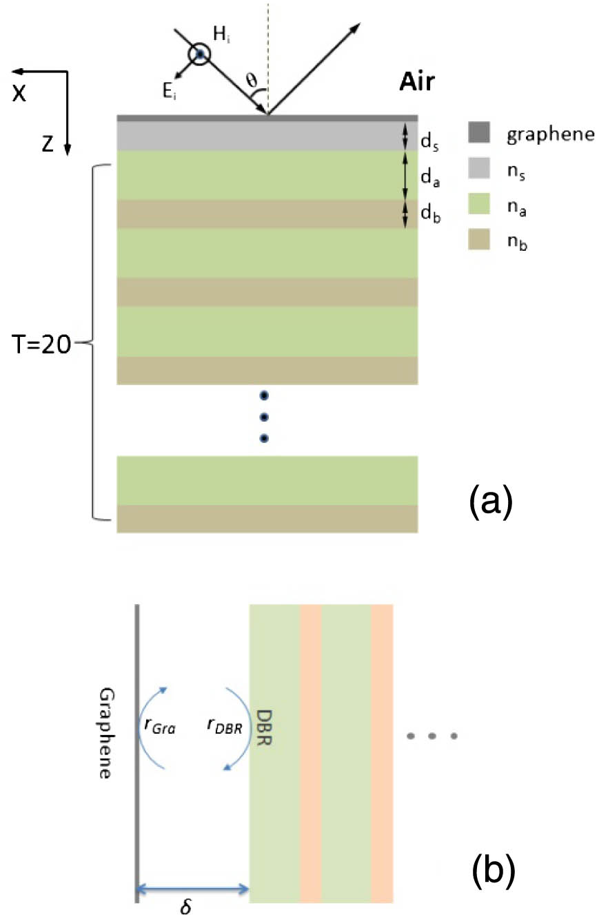
Figure 1.(a) Perfect absorber based on the graphene–1DPC composite structure, and (b) a dissymmetric cavity, enclosed by a sheet of graphene and a DBR.
3. RESULTS AND DISCUSSION
First, we discuss the realization of perfect absorption in the graphene–1DPC composite configuration and the mechanism. In Fig. 2(a), we show the absorption of our structure as a function of frequency for normal incidence. Some of the parameters are , , and . The absorption for 1DPC with twenty periods of dielectrics whose loss can be neglected is almost zero. However, the absorption peak appears at 0.956 THz when a layer of graphene is placed on the top layer. The absorption peak produced by the coupling of incident light and OTSs almost reaches 100%. The full width at half-maximum (FWHM) of the absorption peak is about 0.025 THz, which may find applications in optical switches and directional selective filters. Generally, OTSs can be excited in a metal–DBR configuration. Similarly, perfect absorption may also be realized by replacing the metal with graphene due to its similar properties to metal. In our paper, we only discuss the OTSs for TM polarization for simplicity, though OTSs can be directly excited in both TE- and TM-polarized waves. The excitation conditions for OTSs can be discussed based on Eq. (3). After simplifying the equation, the excitation conditions can be written as follows:

Figure 2.(a) Absorption of the graphene–1DPC configuration (red line is the absorption of our structure without graphene), (b) the phase of (black dotted line), (red dot-dashed line), and (blue line) as a function of frequency, and (c) reflection coefficient for a graphene–top-layer interface (black line), and reflection coefficient for a top-layer–1DPC interface (red line), as a function of frequency.
Figure 2(c) shows the modulus of the reflection coefficient for the electromagnetic wave incident on the graphene layer from the top layer and the reflection coefficient of the electromagnetic wave incident from the same top layer. We can see that the first condition [Eq. (6)] can be well satisfied. When there is no graphene, almost reaches 0, and the OTSs can’t be excited. But the conductive properties of graphene allow a large , which influences the and then satisfies the first condition. For the second condition [Eq. (7)], we also obtain around 0.956 THz, as shown in Fig. 2(b). It perfectly matches the position of the perfect absorption peak. So far, the perfect absorption generated by the excitation of the OTSs has been verified.
To better illustrate the OTSs excited by graphene, we perform a simulation using the transfer matrix method and show the electric field distribution along the axis in the graphene–1DPC composite at 0.956 THz, as shown in Fig. 3. In Fig. 3(a), we show the electric field distribution in the 1DPC composite configuration without the graphene for a better comparison. The calculated electric field is normalized by the incident electric field, and we set the position of the graphene to be . We can see that the electric field in the air is the superposition of the electric fields of the incident and reflected light, which means that total reflection occurs on the interface of the 1DPC. The electric field in the DBR decays exponentially, as the OTSs frequency is in the forbidden band of the DBR. However, it is found that the electric field is strongly enhanced when the graphene is placed on the DBR, as shown in Fig. 3(b). Clearly, there is nearly no electric field of the reflected light in the air, meaning that the incident light is totally absorbed by our structure. In addition, most of the energy of the electric field is concentrated near the interface between the air and the top layer, due to the excitation of the OTSs, which makes it possible to achieve perfect absorption.
Figure 3.(a) Normalized electric field profile distributions in the multilayer configuration without the covering of graphene, and (b) normalized electric field profile distributions in the multilayer configuration with the covering of single-layer graphene.
Next, we discuss the manipulation of the perfect absorption point. We know that the conductivity of graphene can be changed by adjusting the external bias, which can be effectively used in the tunability of our absorber. In addition, the existence of the top layer makes the manipulation more diversified. The absorption peak is blueshifted when we increase the Fermi energy . The Fermi energy is set at 0.75, 0.85, and 0.95 eV, as shown in Fig. 4(a), and all of these values can achieve total absorption. More important, the absorption peak can be manipulated by the Fermi energy of the graphene layer. On the other hand, the theoretical and experimental results show that the OTSs in a metal–Bragg reflector structure can be greatly modulated by the top layer. Thus the eigenfrequency of the OTSs based on graphene–DBR can also be changed by varying the parameters of the top layer. Figure 4(b) shows the different eigenfrequencies of the absorption peak achieved by changing the dielectric constant of the top layer. In addition, the thickness of the top layer has an important impact on absorption. We plot the absorption as a function of frequency with different thicknesses of the top layer, as shown in Fig. 4(c). It can be seen that the reduction of thickness leads to a shift in the absorption peak to a shorter wavelength. Moreover, we can adjust the thickness and dielectric constant of the top layer simultaneously to realize the manipulation of perfect absorption. In Fig. 4(d), the perfect absorption disappears when we set the dielectric constant and thickness to , . However, our graphene–1DPC composite configuration can also achieve perfect absorption after optimizing the thickness of the top layer with the dielectric constant fixed. This adds diversity to the manipulation of perfect absorption devices.
Figure 4.(a) Absorption as a function of frequency at different Fermi energies in the graphene–1DPC composite configuration; the tunability of our absorber based on changing (b) the dielectric constant and (c) thickness of the top layer when ; (d) the tunability based on changing the dielectric constant and thickness of the top layer at the same time.
Another advantage of the proposed structure is that it not only can achieve wide-angle absorption but is insensitive to the polarization state. Figure 5 presents the absorption performance with the angle and frequency of the contour plot in both TM polarization and TE polarization. We can see that the absorption for both polarizations remains almost invariant when the incident angle varies from 0° to 40°, which means that the proposed absorber may be efficient for applications under multidirectional illumination.
Figure 5.Simulated absorption spectra for (a) TE and (b) TM wave as a function of incident angle and frequency. Here, , .
Figure 6.(a) Three and four perfect absorption peaks at the same time; (b) two absorption peaks (red line) and the phase of (blue line) as a function of frequency.
According to the analysis in Fig. 4(c), we can manipulate the perfect absorption peak by changing the thickness of top layer. As the thickness continues to increase, multichannel perfect absorption can be come true. As shown in Fig. 6(a), we can get the absorption rate for more than 98% of the multipeak absorption phenomenon when the thickness is set as or . The FWHM of the multipeak absorption is about 0.006 THz, which suggests the application may have a better effect in a filter due to the narrowband absorption. In our previous article, we explained that the absorption peak is produced due to the excitation of the OTSs. But how can we resolve the multipeak absorption phenomenon? Now, we extend it from a single absorption peak to multipeak absorption, caused by the excitation of multiple OTSs at different eigenfrequencies. Figure 6(b) shows that the double-channel absorption satisfies the phase-matching condition. This indicates that our previous inferences were right. Moreover, the absorption peaks are not independent, but are interrelated. The absorption peak appears periodically when we increase the thickness of the top layer at a fixed incident wavelength. We summed up the relationship between the thickness and absorption peaks, which is for odd peaks and for even peaks, where , , and is the number of absorption peaks. For example, while there is only one absorption peak, that is, , when , 2, 3, 4, 5, it will correspond to five different thicknesses of the top layer, and all of them can realize perfect absorption. Such regulation can be widely utilized in thermal emissions, directional selective filters, and THz optical switches.
Figure 7.(a) Absorption as a function of frequency when the top layer is chosen as fused quartz, , , and the other parameters are the same as in Fig. 2; (b) the manipulation of our absorber based on changing the thickness of the top layer made up of fused quartz; (c) the manipulation of our absorber based on using fused quartz, PTFE, PP, and PET as the top layer, where the thicknesses of these materials are 32, 40, 32, and 24 μm, respectively, and the other parameters are the same as in (a); (d) multichannel absorption when the top layer is chosen as PTFE.
As is well known, the characteristics of loss and dispersion in many dielectrics must be considered when we discuss perfect absorption and manipulation over a wide range of frequencies. Here, considering the feasibility of the actual material, we have chosen several typical materials for the composition of our model. The 1DPC also consists of two kinds of media layers ( and ), namely, polytetrafluoroethylene (PTFE) and fused quartz. Polypropylene (PP) and polyethylene terephthalate (PET) are used for tuning the position of perfect absorption as the top layer. The dielectric constant for different frequencies of those materials can be described by the Debye model [30] as follows: where is the complex dielectric function, is the frequency, is the relaxation time, is the static permittivity, and is the high frequency dielectric constant. The parameters of these materials can be found in the related literature [30–33]. After considering the loss and dispersion, our structure can also achieve perfect absorption when the top layer is chosen as fused quartz, and the position of perfect absorption can be tuned by changing the thickness of the top layer, as shown in Figs. 7(a) and 7(b). Furthermore, the manipulation can be achieved by varying the dielectric constant of the top layer. In this paper, we choose fused quartz, PTFE, PP, and PET as the top layer, whose complex dielectric constants are described by the Debye model, as shown in Fig. 7(c). Moreover, in Fig. 7(d), dual channels or three channels can also be obtained, which match well with the previous discipline shown in Fig. 6. It is obvious that perfect absorption and manipulation can be realized even when the loss and dispersion of the actual materials are considered.
4. CONCLUSIONS
In summary, we have proposed an effective method for realizing perfect absorption in the THz frequency regime based on a graphene–1DPC structure by the transfer matrix method. As a result of the intense coupling of incident light and OTSs at the interface of the graphene and the DBR, a strong absorption occurs in our system. We can achieve tunability of the absorption peak by changing the Fermi energy applied to the graphene sheets. Moreover, the thickness and dielectric constant of the top layer are another option to achieve the manipulation of perfect absorption. In addition, it is found that the absorption performance of the proposed structure is wide-angle and polarization-insensitive. More importantly, we can produce multichannel narrow-peak absorption at the same time, and the relationship between the thickness and multichannel absorption has been summarized. Finally, we demonstrated that perfect absorption, manipulation, and multichannel absorption can be achieved even when the loss and dispersion are taken into account. We believe that our work in this paper will have potential applications in narrowband selective filters, solar photovoltaic cells, thermal emissions, and optical detection devices.
References
[1] J. Federici, L. Moeller. Review of terahertz and subterahertz wireless communications. J. Appl. Phys., 107, 111101(2010).
[2] P. U. Jepsen, D. G. Cooke, M. Koch. Terahertz spectroscopy and imaging—modern techniques and applications. Laser Photon. Rev., 5, 124-166(2011).
[3] M. Tonouchi. Cutting-edge terahertz technology. Nat. Photonics, 1, 97-105(2007).
[4] S. Thongrattanasiri, F. H. L. Koppens, F. J. G. de Abajo. Complete optical absorption in periodically patterned graphene. Phys. Rev. Lett., 108, 047401(2012).
[5] Y. Xiang, X. Dai, J. Guo, H. Zhang, S. Wen, D. Tang. Critical coupling with graphene-based hyperbolic metamaterials. Sci. Rep., 4, 5483(2014).
[6] M. Diem, T. Koschny, C. M. Soukoulis. Wide-angle perfect absorber/thermal emitter in the terahertz regime. Phys. Rev. B, 79, 033101(2009).
[7] H. Wu, F. Shi, Y. Chen. Broadband terahertz absorption enabled by coating an ultrathin antireflection film on doped semiconductor. Opt. Express, 24, 20663-20671(2016).
[8] J. Zhou, K. Bhattarai, S. Silva, J. Jeon, J. Kim. A THz plasmonics perfect absorber and Fabry–Perot cavity mechanism (Conference Presentation). Proc. SPIE, 9956, 99560H(2016).
[9] N. I. Landy, C. M. Bingham, T. Tyler, N. Jokerst, D. R. Smith, W. J. Padilla. Design, theory, and measurement of a polarization-insensitive absorber for terahertz imaging. Phys. Rev. B, 79, 125104(2009).
[10] T. V. Teperik, F. J. G. de Abajo, A. G. Borisov, M. Abdelsalam, P. N. Bartlett, Y. Sugawara, J. J. Baumberg. Omnidirectional absorption in nanostructured metal surfaces. Nat. Photonics, 2, 299-301(2008).
[11] B. Zhu, Z. Wang, C. Huang, Y. Feng, J. Zhao, T. Jiang. Polarization insensitive metamaterial absorber with wide incident angle. Prog. Electromagn. Res., 101, 231-239(2010).
[12] A. V. Kavokin, I. A. Shelykh, G. Malpuech. Lossless interface modes at the boundary between two periodic dielectric structures. Phys. Rev. B, 72, 233102(2005).
[13] M. Kaliteevski, I. Iorsh, S. Brand, R. A. Abram, J. M. Chamberlain, A. V. Kavokin, I. A. Shelykh. Tamm plasmon-polaritons: possible electromagnetic states at the interface of a metal and a dielectric Bragg mirror. Phys. Rev. B, 76, 165415(2007).
[14] S. Brand, M. A. Kaliteevski, R. A. Abram. Optical Tamm states above the bulk plasma frequency at a Bragg stack/metal interface. Phys. Rev. B, 79, 085416(2009).
[15] X. F. Chen, S. J. Li, Y. Zhang. The wide-angle perfect absorption based on the optical Tamm states. Optoelectron. Lett., 10, 317-320(2014).
[16] S. Lu, X. Chao, X. Chen, B. Tang. TE polarization perfect absorption with dual-band in metal-photonic crystal-metal structure. Acta Opt. Sin., 35, 289-294(2015).
[17] M. S. Fang, F. H. Shi, Y. H. Chen. Unidirectional all-optical absorption switch based on optical Tamm state in nonlinear plasmonic waveguide. Plasmonics, 11, 197-203(2015).
[18] A. K. Geim, K. S. Novoselov. The rise of graphene. Nat. Mater., 6, 183-191(2007).
[19] K. S. Novoselov, V. I. Fal’ko, L. Colombo, P. R. Gellert, M. G. Schwab, K. Kim. A roadmap for graphene. Nature, 490, 192-200(2012).
[20] F. Bonaccorso, Z. Sun, T. Hasan, A. C. Ferrari. Graphene photonics and optoelectronics. Nat. Photonics, 4, 611-622(2010).
[21] G. Lu, K. Yu, Z. Wen, J. Chen. Semiconducting graphene: converting graphene from semimetal to semiconductor. Nanoscale, 5, 1353-1368(2013).
[22] P. Tassin, T. Koschny, M. Kafesaki, C. M. Soukoulis. A comparison of graphene, superconductors and metals as conductors for metamaterials and plasmonics. Nat. Photonics, 6, 259-264(2012).
[23] M. Grande, M. A. Vincenti, T. Stomeo, G. V. Bianco, D. de Ceglia, N. Aközbek, V. Petruzzelli, G. Bruno, M. De Vittorio, M. Scalora, A. D’Orazio. Graphene-based absorber exploiting guided mode resonances in one-dimensional gratings. Opt. Express, 22, 31511-31519(2014).
[24] J. Guo, Y. Sun, Y. Zhang, H. Li, H. Jiang, H. Chen. Experimental investigation of interface states in photonic crystal heterostructures. Phys. Rev. E, 78, 026607(2008).
[25] M. E. Sasin, R. P. Seisyan, M. A. Kalitteevski, S. Brand, R. A. Abram, J. M. Chamberlain, A. Y. Egorov, A. P. Vasilev, V. S. Mikhrin, A. V. Kavokin. Tamm plasmon polaritons: slow and spatially compact light. Appl. Phys. Lett., 92, 251112(2008).
[26] M. Tamagnone, J. S. Gomez-Diaz, J. R. Mosig. Analysis and design of terahertz antennas based on plasmonic resonant graphene sheets. J. Appl. Phys., 112, 114915(2012).
[27] B. Auguié, A. Bruchhausen, A. Fainstein. Critical coupling to Tamm plasmons. J. Opt., 17, 035003(2015).
[28] K. Bliokh, Y. Bliokh, V. Freilikher, S. Savel’ev, F. Nori. Unusual resonators: plasmonics, metamaterials, and random media. Rev. Mod. Phys., 80, 1201-1213(2008).
[29] T. Zhan, X. Shi, Y. Dai, X. Liu, J. Zi. Transfer matrix method for optics in graphene layers. J. Phys., 25, 215301(2013).
[30] N. Nagai, R. Fukasawa. Abnormal dispersion of polymer films in the THz frequency region. Chem. Phys. Lett., 388, 479-482(2004).
[31] M. Naftaly, R. E. Miles. Terahertz time-domain spectroscopy: a new tool for the study of glasses in the far infrared. J. Non-Cryst. Solids, 351, 3341-3346(2005).
[32] C. M. Randall, R. D. Rawcliffe. Refractive indices of germanium, silicon, and fused quartz in the far infrared. Appl. Opt., 6, 1889-1895(1967).
[33] X. L. Cheng, X. Chen, Z. Y. Zhu. THz-TDS spectra study of polymer materials with different polarity. J. Infrared Millimeter Waves, 32, 150-153(2013).


