• Photonics Research
  • Vol. 11, Issue 3, 393 (2023)
Ying Xu1、†, Weiye Zhang1、†, and Chuanshan Tian*
Author Affiliations
  • Department of Physics, Fudan University, Shanghai 200438, China
  • show less
    DOI: 10.1364/PRJ.471266 Cite this Article Set citation alerts
    Ying Xu, Weiye Zhang, Chuanshan Tian. Recent advances on applications of NV magnetometry in condensed matter physics[J]. Photonics Research, 2023, 11(3): 393 Copy Citation Text show less
    Properties of the nitrogen-vacancy center. (a) Illustration of the nitrogen-vacancy center and diamond lattice. Transparent, the vacancy; blue, the substitutional nitrogen atom; black, carbon atoms. (b) Relevant electronic energy levels of NV−. The NV− center is excited by 532 nm laser pulses off-resonantly (green arrow), and fluorescent photons from ∼600 to ∼800 nm are collected (red arrow). The strong (weak) intersystem crossings between spin-triplet states and spin-singlet states (E3→A11, E1→A23) are denoted by solid black (dashed gray) arrows. The spin states in the ground state (A23) can be manipulated by microwave (MW) excitation.
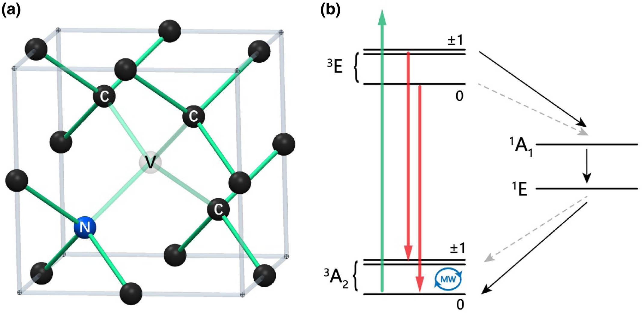
    Fig. 1. Properties of the nitrogen-vacancy center. (a) Illustration of the nitrogen-vacancy center and diamond lattice. Transparent, the vacancy; blue, the substitutional nitrogen atom; black, carbon atoms. (b) Relevant electronic energy levels of NV. The NV center is excited by 532 nm laser pulses off-resonantly (green arrow), and fluorescent photons from 600 to 800  nm are collected (red arrow). The strong (weak) intersystem crossings between spin-triplet states and spin-singlet states (E3A11, E1A23) are denoted by solid black (dashed gray) arrows. The spin states in the ground state (A23) can be manipulated by microwave (MW) excitation.
    Principle of spin to charge conversion readout. (a) High fidelity charge-state determination of NVs. During each readout, NV− statically emits far more photons than NV0 as shown by the blue histogram. The charge-state determination of NVs is realized by setting a threshold indicated by the red dashed line. The photon readout rate from NV0 becomes negligible above the threshold. Adapted from Ref. [55]. (b) Schematic of the spin-to-charge conversion readout protocol used in Ref. [38]. Adapted from Ref. [57].
    Fig. 2. Principle of spin to charge conversion readout. (a) High fidelity charge-state determination of NVs. During each readout, NV statically emits far more photons than NV0 as shown by the blue histogram. The charge-state determination of NVs is realized by setting a threshold indicated by the red dashed line. The photon readout rate from NV0 becomes negligible above the threshold. Adapted from Ref. [55]. (b) Schematic of the spin-to-charge conversion readout protocol used in Ref. [38]. Adapted from Ref. [57].
    Methods to improve photon collection rate. (a) Schematic of high efficiency side collection with coupling prisms on four sides of the diamond. Reprinted with permission from Ref. [55]. Copyright 2016 American Physical Society. (b) Schematic of the parabolic collector. 65% of the photons emitted from the NVs are coupled to the concentrator according to simulation. Adapted from Ref. [63]. (c) Illustration of an array of diamond circular bullseye gratings adjacent to a microwave (MW) strip line. Reprinted with permission from Ref. [65]. Copyright 2015 American Chemical Society. (d) SEM image of the nanopillar, consisting of parabolic tip and tapered waveguide. Reprinted with permission from Ref. [64]. Copyright 2020 American Physical Society.
    Fig. 3. Methods to improve photon collection rate. (a) Schematic of high efficiency side collection with coupling prisms on four sides of the diamond. Reprinted with permission from Ref. [55]. Copyright 2016 American Physical Society. (b) Schematic of the parabolic collector. 65% of the photons emitted from the NVs are coupled to the concentrator according to simulation. Adapted from Ref. [63]. (c) Illustration of an array of diamond circular bullseye gratings adjacent to a microwave (MW) strip line. Reprinted with permission from Ref. [65]. Copyright 2015 American Chemical Society. (d) SEM image of the nanopillar, consisting of parabolic tip and tapered waveguide. Reprinted with permission from Ref. [64]. Copyright 2020 American Physical Society.
    Super-resolution microscopy techniques in NV− magnetometry. (a) Schematic of the Spin-RESOLFT protocol used by Jaskula et al. The selective manipulation of the NV spin state is realized by a 532 nm doughnut beam. Reprinted with permission from Ref. [104]. Copyright 2017 Optical Society of America. (b) Schematic of the charge state depletion microscopy configuration. The 532 and 637 nm lasers were used to initialize and switch the charge state of NVs, and the 589 nm laser is for the charge state readout. The lasers and fluorescence emission were combined and split using three long-pass dichroic mirrors (DMs). The fluorescence of NV− was detected by avalanche photodiode (APD2) with a long-pass filter (LP), and the fluorescence of NV0 was detected by APD1 with a short-pass filter (SP). Two phase masks were used to produce the doughnut-shaped laser beams. Reprinted with permission from Ref. [106]. Copyright 2015 Macmillan Publishers Ltd. (c) Exemplary fluorescence time trace recorded with an APD. Three count levels indicate 0–2 NVs are excited during each CCD exposure. Only those frames with one excited NV were chosen to reconstruct the super-resolution image. Adapted from Ref. [107].
    Fig. 4. Super-resolution microscopy techniques in NV magnetometry. (a) Schematic of the Spin-RESOLFT protocol used by Jaskula et al. The selective manipulation of the NV spin state is realized by a 532 nm doughnut beam. Reprinted with permission from Ref. [104]. Copyright 2017 Optical Society of America. (b) Schematic of the charge state depletion microscopy configuration. The 532 and 637 nm lasers were used to initialize and switch the charge state of NVs, and the 589 nm laser is for the charge state readout. The lasers and fluorescence emission were combined and split using three long-pass dichroic mirrors (DMs). The fluorescence of NV was detected by avalanche photodiode (APD2) with a long-pass filter (LP), and the fluorescence of NV0 was detected by APD1 with a short-pass filter (SP). Two phase masks were used to produce the doughnut-shaped laser beams. Reprinted with permission from Ref. [106]. Copyright 2015 Macmillan Publishers Ltd. (c) Exemplary fluorescence time trace recorded with an APD. Three count levels indicate 0–2 NVs are excited during each CCD exposure. Only those frames with one excited NV were chosen to reconstruct the super-resolution image. Adapted from Ref. [107].
    Probing statistic magnetic structures in AFM/FM materials. (a) Determination of DW structure in ferromagnetic materials. Left, schematic side view of a DW in a perpendicularly magnetized film. The DW structure can be characterized by the angle Ψ of the internal magnetization indicated by the black arrows, while the stray field above the film represented by the gray arrows varies for different DW structures. Middle and right, calculated stray field components Bx and Bz at a distance d=120 nm above the magnetic layer for DW of width ∼20 nm, centered at x=0. Reprinted with permission from Ref. [81]. Copyright 2015 Macmillan Publishers Ltd. (b) Reconstruction of magnetization of a skyrmion in an FM thin film. The upper sheet represents Bz component of the stray field for a skyrmion nucleated at the center of the magnetic disc, while the lower sheet is the reconstructed mz component on the film. The black dashed lines represent the boundary of the disc. Scale bar, 300 nm. Reprinted with permission from Ref. [83]. Copyright 2018 Macmillan Publishers Ltd. (c) Real-space imaging of non-collinear antiferromagnetic order above the BiFeO3 film while operating the NV− magnetometer in dual-iso-B imaging mode. The dual-iso-B signal S=PL(v2)−PL(v1) corresponds to the difference in photoluminescence (PL) intensity for two fixed RF frequencies. The periodic variation of the magnetic stray field is caused by the cycloidal modulation of the spin order. The black dashed guidelines represent ferroelectric domain walls separating regions of different cycloidal propagation vector. Reprinted with permission from Ref. [76]. Copyright 2017 Macmillan Publishers Ltd.
    Fig. 5. Probing statistic magnetic structures in AFM/FM materials. (a) Determination of DW structure in ferromagnetic materials. Left, schematic side view of a DW in a perpendicularly magnetized film. The DW structure can be characterized by the angle Ψ of the internal magnetization indicated by the black arrows, while the stray field above the film represented by the gray arrows varies for different DW structures. Middle and right, calculated stray field components Bx and Bz at a distance d=120  nm above the magnetic layer for DW of width 20  nm, centered at x=0. Reprinted with permission from Ref. [81]. Copyright 2015 Macmillan Publishers Ltd. (b) Reconstruction of magnetization of a skyrmion in an FM thin film. The upper sheet represents Bz component of the stray field for a skyrmion nucleated at the center of the magnetic disc, while the lower sheet is the reconstructed mz component on the film. The black dashed lines represent the boundary of the disc. Scale bar, 300 nm. Reprinted with permission from Ref. [83]. Copyright 2018 Macmillan Publishers Ltd. (c) Real-space imaging of non-collinear antiferromagnetic order above the BiFeO3 film while operating the NV magnetometer in dual-iso-B imaging mode. The dual-iso-B signal S=PL(v2)PL(v1) corresponds to the difference in photoluminescence (PL) intensity for two fixed RF frequencies. The periodic variation of the magnetic stray field is caused by the cycloidal modulation of the spin order. The black dashed guidelines represent ferroelectric domain walls separating regions of different cycloidal propagation vector. Reprinted with permission from Ref. [76]. Copyright 2017 Macmillan Publishers Ltd.
    Probing magnetic excitations in magnetic insulators. (a) Imaging coherent spin-waves. The pattern is generated by the interference between the stray field and an external spatially homogeneous field BREF with the same frequency. Top, spatial ESR contrast at a bias field B0=25 mT when a spin-wave of frequency equal to ESR frequency ωSW=ω−=2π×2.17 GHz is excited by a microwave current in the stripline. Scale bar, 20 μm. Bottom, Rabi frequency ωRabi/2 versus distance from the stripline when ωSW=ω−=2π×2.11 GHz and B0=27 mT. Red line, fitted Rabi frequency according to a model including the field of the stripline, the bonding wire, and the spin-waves. Inset, measurement sequence. Reprinted with permission from Ref. [157]. Copyright 2020 AAAS. (b) The spin chemical potential (μ) in YIG as a function of drive power (BAC2) and external bias field (BEXT). μ saturates at the minimum of the magnon band set by the FMR frequency. Reprinted with permission from Ref. [168]. Copyright 2017 AAAS.
    Fig. 6. Probing magnetic excitations in magnetic insulators. (a) Imaging coherent spin-waves. The pattern is generated by the interference between the stray field and an external spatially homogeneous field BREF with the same frequency. Top, spatial ESR contrast at a bias field B0=25  mT when a spin-wave of frequency equal to ESR frequency ωSW=ω=2π×2.17  GHz is excited by a microwave current in the stripline. Scale bar, 20 μm. Bottom, Rabi frequency ωRabi/2 versus distance from the stripline when ωSW=ω=2π×2.11  GHz and B0=27  mT. Red line, fitted Rabi frequency according to a model including the field of the stripline, the bonding wire, and the spin-waves. Inset, measurement sequence. Reprinted with permission from Ref. [157]. Copyright 2020 AAAS. (b) The spin chemical potential (μ) in YIG as a function of drive power (BAC2) and external bias field (BEXT). μ saturates at the minimum of the magnon band set by the FMR frequency. Reprinted with permission from Ref. [168]. Copyright 2017 AAAS.
    Determination of superconductivity by NV− magnetometry. (a) Detection of ac Meissner effect on an ultrathin micron-size BSSCO film. The BSSCO flake was exfoliated on the diamond chip with NV− implanted at the surface. The yellow arrow represents the GHz current flowing in the central copper conductor. The orange arrows represent the direction of the microwave magnetic field. The 532 nm laser beam is normally incident. (b) Comparison of the measured (red dots) and calculated magnetic field (colored lines) expelled by the 33 nm thick BSSCO film versus temperature. The calculation is based on the two-fluid model, and the brown and blue curves show the results with λ assumed to be 230 and 250 nm, respectively. Resistance of the thin film versus temperature (black line) is shown for reference. (a), (b) Reprinted with permission from Ref. [52]. Copyright 2019 American Chemical Society.
    Fig. 7. Determination of superconductivity by NV magnetometry. (a) Detection of ac Meissner effect on an ultrathin micron-size BSSCO film. The BSSCO flake was exfoliated on the diamond chip with NV implanted at the surface. The yellow arrow represents the GHz current flowing in the central copper conductor. The orange arrows represent the direction of the microwave magnetic field. The 532 nm laser beam is normally incident. (b) Comparison of the measured (red dots) and calculated magnetic field (colored lines) expelled by the 33 nm thick BSSCO film versus temperature. The calculation is based on the two-fluid model, and the brown and blue curves show the results with λ assumed to be 230 and 250 nm, respectively. Resistance of the thin film versus temperature (black line) is shown for reference. (a), (b) Reprinted with permission from Ref. [52]. Copyright 2019 American Chemical Society.
    Determination of superconductivity at high pressure by NV− magnetometry. (a) Left, illustration of the diamond anvil cell (DAC) geometry. Two opposing anvils are compressed by a nonmagnetic steel cell and cubic boron nitride backing plates (gray). Top right, The DAC chamber loaded with the sample, a pressure-transmitting medium, and a single ruby microsphere for pressure calibration. A layer of NV− centers near the surface is embedded into the diamond anvil at the bottom. Bottom right, a representative ODMR spectrum of an ensemble of NV− centers. Four splitting groups are presented due to the four possible orientations of NV− axes that result in different magnetic field projection cases. Reprinted with permission from Ref. [176]. Copyright 2019 AAAS. (b) Maps of the ODMR frequency splitting above the MgB2 sample for different temperatures at a bias field B0≈1.8 mT. Below 30 K, expelling of the magnetic flux is observed and disappears above 30 K, indicating a transition from a superconducting state to a normal state. Top left, optical image of the sample. The red square marks the area where the ODMR splitting is mapped. Reprinted with permission from Ref. [31]. Copyright 2019 AAAS.
    Fig. 8. Determination of superconductivity at high pressure by NV magnetometry. (a) Left, illustration of the diamond anvil cell (DAC) geometry. Two opposing anvils are compressed by a nonmagnetic steel cell and cubic boron nitride backing plates (gray). Top right, The DAC chamber loaded with the sample, a pressure-transmitting medium, and a single ruby microsphere for pressure calibration. A layer of NV centers near the surface is embedded into the diamond anvil at the bottom. Bottom right, a representative ODMR spectrum of an ensemble of NV centers. Four splitting groups are presented due to the four possible orientations of NV axes that result in different magnetic field projection cases. Reprinted with permission from Ref. [176]. Copyright 2019 AAAS. (b) Maps of the ODMR frequency splitting above the MgB2 sample for different temperatures at a bias field B01.8  mT. Below 30 K, expelling of the magnetic flux is observed and disappears above 30 K, indicating a transition from a superconducting state to a normal state. Top left, optical image of the sample. The red square marks the area where the ODMR splitting is mapped. Reprinted with permission from Ref. [31]. Copyright 2019 AAAS.
    Characteristic of superconductors investigated by NV− magnetometry. (a) Measurements of the onset of the magnetic field penetration Hp on single crystal film of YBa2Cu3O7−δ. The inset shows the superconducting phase transition by measuring magnetic field screening in zero field cooling scheme, with transition temperature Tc≈88 K. Reprinted with permission from Ref. [175]. Copyright 2019 American Physical Society. (b) NV− magnetometry image of vortices in the superconductor BaFe2(As0.7P0.3)2 at T=6 K. The vortices were formed by field cooling the sample to temperature below its Tc (∼30 K) with an external field of 10 G. Dark areas in the image correspond to locations where the penetrated field has a magnitude of ∼5.9 G (resonant with a 2862 MHz RF field) along the axis of the NV center. Scale bar, 400 nm. Reprinted with permission from Ref. [26]. Copyright 2016 Macmillan Publishers Ltd. (c) Image of the magnetic stray field emanating from a single vortex in a YBCO film with a thickness of ∼100 nm, obtained with the scanning probe NV− magnetometer. (d) Line profile of the magnetic field magnitude along a horizontal line above the YBCO film with a thickness of 150 nm, as shown in the insets. Blue and green dashed lines represent the best fittings to a Pearl vortex and a magnetic monopole. The bulk London penetration depth λ=251±14 nm can be obtained from the fitting of Pearl vortex. (c) and (d) Reprinted with permission from Ref. [27]. Copyright 2016 Macmillan Publishers Ltd.
    Fig. 9. Characteristic of superconductors investigated by NV magnetometry. (a) Measurements of the onset of the magnetic field penetration Hp on single crystal film of YBa2Cu3O7δ. The inset shows the superconducting phase transition by measuring magnetic field screening in zero field cooling scheme, with transition temperature Tc88  K. Reprinted with permission from Ref. [175]. Copyright 2019 American Physical Society. (b) NV magnetometry image of vortices in the superconductor BaFe2(As0.7P0.3)2 at T=6  K. The vortices were formed by field cooling the sample to temperature below its Tc (30  K) with an external field of 10 G. Dark areas in the image correspond to locations where the penetrated field has a magnitude of 5.9  G (resonant with a 2862 MHz RF field) along the axis of the NV center. Scale bar, 400 nm. Reprinted with permission from Ref. [26]. Copyright 2016 Macmillan Publishers Ltd. (c) Image of the magnetic stray field emanating from a single vortex in a YBCO film with a thickness of 100  nm, obtained with the scanning probe NV magnetometer. (d) Line profile of the magnetic field magnitude along a horizontal line above the YBCO film with a thickness of 150 nm, as shown in the insets. Blue and green dashed lines represent the best fittings to a Pearl vortex and a magnetic monopole. The bulk London penetration depth λ=251±14  nm can be obtained from the fitting of Pearl vortex. (c) and (d) Reprinted with permission from Ref. [27]. Copyright 2016 Macmillan Publishers Ltd.
    Probing electron transport phenomena in metals/semimetals by NV− magnetometry. (a) Illustration of mapping current density in the carbon nanotubes with the scanning NV− magnetometer. A diamond nanoparticle hosting a single NV− center is grafted onto the scanning tip of an atomic force microscope. During the detection, the nanoparticle is positioned at a distance less than 100 nm from a current-carrying carbon nanotube. The ESR frequency of the NV− center is continuously monitored with the optical fluorescence collected by an objective (not shown). Reprinted with permission from Ref. [97]. Copyright 2017 American Chemical Society. (b) Mapping the viscous electron flow in graphene. The boundary of the graphene device is marked by red lines. Current is injected from the source (top), and the black arrows at the top and bottom left of the figure illustrate the current flow. 2D current density J=(Jx,Jy) reconstructed from the vector magnetic field detected by the wide-field NV− magnetometer is plotted, with the direction indicated by black arrows and the amplitude indicated by color. The reconstructed flow pattern is consistent with the injected current. The gray area is covered by a metallic top-gate contact that obstructs light. (c) Current profiles across the graphene device reconstructed from the stray field measured by the scanning NV− magnetometer. Current density Jy(x) is normalized by the average 2D current density, where I is the total current and W is the width of the channel (1 μm for the graphene devices and 800 nm for the palladium electrode). Red dots, graphene at the charge-neutrality point (CNP); gray dots, palladium electrode; orange dots, low-mobility graphene. Blue (green) lines are calculated current density for ideal viscous (uniform) flow with 5% error band. (b) and (c) Reprinted with permission from Ref. [207]. Copyright 2020 Macmillan Publishers Ltd. (d) Spatial mapping of the local magnetic noise at current density J=0.18 mA/μm and carrier density n=0.92×1012 cm−2. The spatial profile is consistent with the exponential growth of phonons due to Cerenkov amplification (cartoon, top). The dashed black curve shows the theoretically predicted excess phonon population (offset to account for background noise). a.u., arbitrary unit. Reprinted with permission from Ref. [208]. Copyright 2019 AAAS.
    Fig. 10. Probing electron transport phenomena in metals/semimetals by NV magnetometry. (a) Illustration of mapping current density in the carbon nanotubes with the scanning NV magnetometer. A diamond nanoparticle hosting a single NV center is grafted onto the scanning tip of an atomic force microscope. During the detection, the nanoparticle is positioned at a distance less than 100 nm from a current-carrying carbon nanotube. The ESR frequency of the NV center is continuously monitored with the optical fluorescence collected by an objective (not shown). Reprinted with permission from Ref. [97]. Copyright 2017 American Chemical Society. (b) Mapping the viscous electron flow in graphene. The boundary of the graphene device is marked by red lines. Current is injected from the source (top), and the black arrows at the top and bottom left of the figure illustrate the current flow. 2D current density J=(Jx,Jy) reconstructed from the vector magnetic field detected by the wide-field NV magnetometer is plotted, with the direction indicated by black arrows and the amplitude indicated by color. The reconstructed flow pattern is consistent with the injected current. The gray area is covered by a metallic top-gate contact that obstructs light. (c) Current profiles across the graphene device reconstructed from the stray field measured by the scanning NV magnetometer. Current density Jy(x) is normalized by the average 2D current density, where I is the total current and W is the width of the channel (1 μm for the graphene devices and 800 nm for the palladium electrode). Red dots, graphene at the charge-neutrality point (CNP); gray dots, palladium electrode; orange dots, low-mobility graphene. Blue (green) lines are calculated current density for ideal viscous (uniform) flow with 5% error band. (b) and (c) Reprinted with permission from Ref. [207]. Copyright 2020 Macmillan Publishers Ltd. (d) Spatial mapping of the local magnetic noise at current density J=0.18  mA/μm and carrier density n=0.92×10¹²  cm2. The spatial profile is consistent with the exponential growth of phonons due to Cerenkov amplification (cartoon, top). The dashed black curve shows the theoretically predicted excess phonon population (offset to account for background noise). a.u., arbitrary unit. Reprinted with permission from Ref. [208]. Copyright 2019 AAAS.
    Scheme (Resolution)Atomic Force Microscope (10–100 nm)Confocal (500  nm)Large Ensemble (mm)
    dc magnetometry310  μT/Hz1/2 [26,27,76,8186]0.033  μT/Hz1/2 [8789]15  pT/Hz1/2 [80]
    ac magnetometry50100  nT/Hz1/2 [23,74,90]4100  nT/Hz1/2 [91,92]1  pT/Hz1/2 [63]
    Table 1. Typical Spatial Resolution and Sensitivity of NV Magnetometry Available for Condensed Matter Systems Researcha
    Ying Xu, Weiye Zhang, Chuanshan Tian. Recent advances on applications of NV magnetometry in condensed matter physics[J]. Photonics Research, 2023, 11(3): 393
    Download Citation