Measuring magnetic response from spin and current is of fundamental interest in condensed matter physics. Negatively charged nitrogen-vacancy () centers in diamond are emerging as a robust and versatile quantum sensor owing to their high sensitivity, nanometer-scale spatial resolution, and noninvasive operation with access to static and dynamic magnetic and electron transport properties. In this review, we discuss the rapidly growing interest in the implementation of magnetometry to explore condensed matter physics, focusing on three topics: anti/ferromagnetic materials, superconductors, and metals/semimetals/semiconductors.
1. INTRODUCTION
Many new materials displaying exciting physical phenomena have been discovered and explored in the past decades. Examples include novel superconductors (SCs) [1–3], van der Waals materials [4,5], topological insulators [6,7], and multiferroic materials [8,9]. The emergence of these new systems challenges traditional measurement schemes in characterizing their magnetic properties in terms of sensitivity, spatial resolution, dynamic range, etc. Generally, the characterization of condensed matter materials with magnetometry [10,11] mainly focuses on probing four types of magnetic fields generated by spins and currents [11]: (1) static spin configuration of a magnetic system, such as domain wall (DW) and skyrmion; (2) dynamic field produced by the excitations of magnetic systems, e.g., spin-wave; (3) field generated by static current distributions; and (4) field noise created by current fluctuations. Various magnetic measurement schemes have been proposed for different needs. Spin-resolved magnetometric techniques, such as muon spectroscopy [12], nuclear magnetic resonance (NMR) [13,14], and neutron scattering [15], enable noninvasive wide-field measurement of the magnetic structure of a material. On the other hand, scanning probe-based approaches, such as magnetic force microscopy (MFM) [16,17] and scanning superconducting quantum interference devices (scanning SQUIDs) [10,18], allow real-space imaging of the magnetic fields emanating from nanoscale samples. However, the spin-resolved techniques offer a poor spatial resolution that cannot resolve nanoscale magnetic structure, while the scanning techniques either act as perturbative probes or can only work over a narrow temperature range. The electronic spin of the negatively charged nitrogen-vacancy () center in diamond is emerging as a robust and versatile quantum sensor for noninvasive detection of weak magnetic fields [19]. Since the pioneering works [20–22], magnetometry has demonstrated its unique advantages in comparison to other magnetic-sensing techniques: single-electron and individual-proton sensitivity [23,24], nanometer-scale spatial resolution [25], and high tolerance of working temperature [26–28] (from to above room temperature) and pressure [29–32] (from ultra-high vacuum to ).
In this review, we outline some recent advances in magnetometry and its applications in the study of magnetic and transport properties in condensed matter systems. We begin with a summary of the properties and experimental techniques. Next, we discuss the implementation of magnetometry to study magnetic phenomena in condensed matter materials with emphasis on anti/ferrimagnetism, SC, and metal/semimetal/semiconductors. In the case of antiferrimagnetic/ferrimagnetic materials, the high spatial resolution of the magnetometry was used to determine the nature of antiferromagnetic/ferromagnetic (AFM/FM) spin textures. Meanwhile, the high spectral resolution of magnetometry was employed in the study of spin-waves in FM materials. In the following section, we discuss the application of magnetometry in SCs. Owing to its merit of operation under a broad range of temperatures and pressures, magnetometry is a unique tool to determine the transition temperature and the critical field, and to map the spatial structure of magnetic responses in various superconducting materials. Finally, we focus on the dc and dynamic magnetic field created by current flow or fluctuations in metal/semimetal/semiconductor nanostructures and thin films. In this aspect, the noninvasive magnetometry with high-spatial resolution finds its unique advantage in mapping distribution of the local current density and its fluctuation.
2. PRINCIPLES OF MAGNETOMETRY
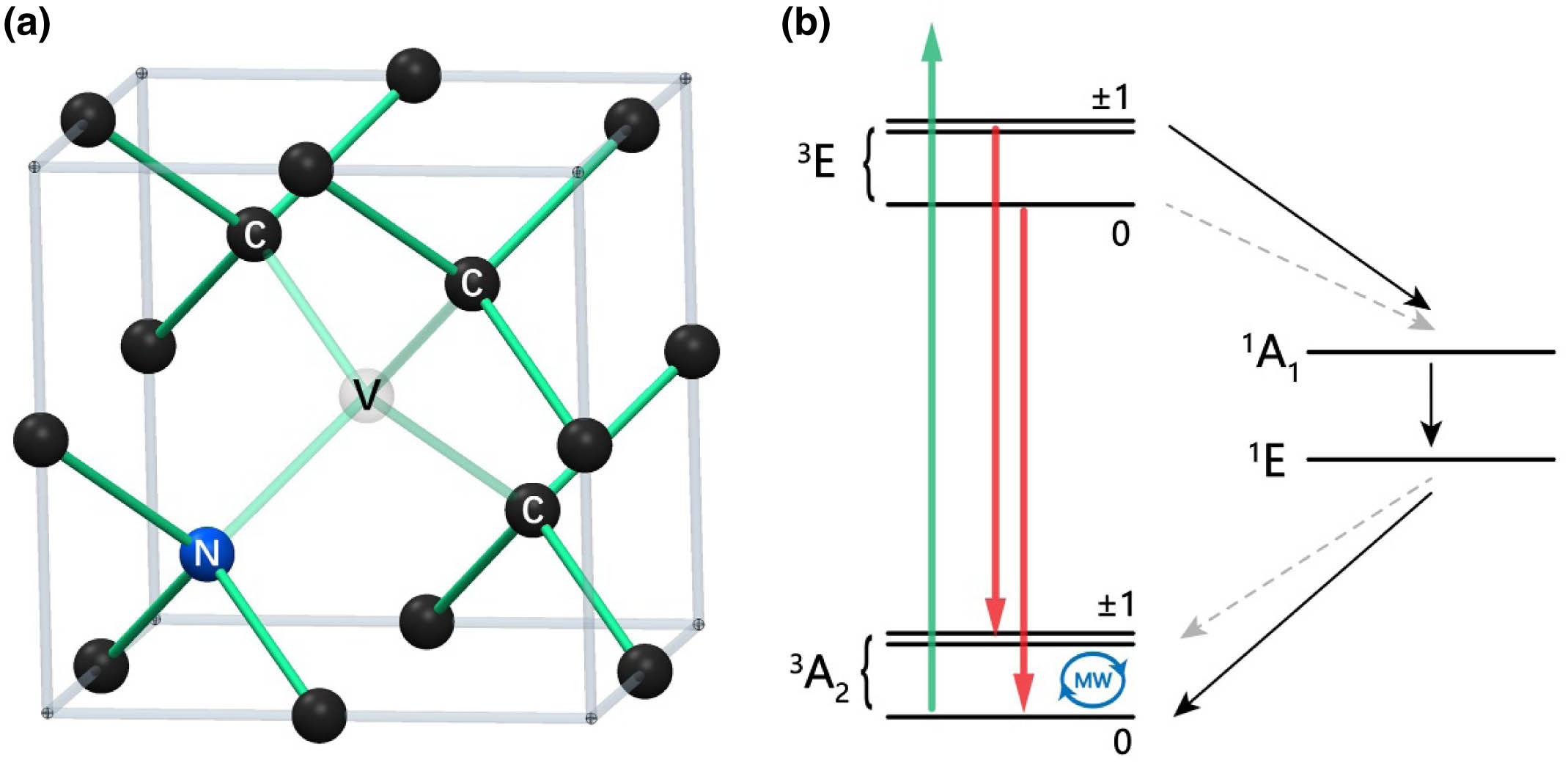
The properties and measurement schemes of centers have been summarized in some well-noted review papers [11,19,33–36]. Here we briefly outline the fundamental properties and some basic center measurement schemes to clarify nomenclatures in the following discussion. The center is a type of point defect in the diamond lattice [Fig. 1(a)] with its energy-level structure shown in Fig. 1(b). At present, most of the experiments on centers are carried out via manipulation and detection of electron spins in the ground state (GS) . The electron spins are first initialized to through off-resonant optical excitation. Then, the spins are actively controlled by resonant microwave pulses, and the environmental magnetic information is encoded into the spin states. Finally, the population of electrons in different spin states is read out by fluorescence difference because the photoluminescence efficiency of electrons in states is 30% lower than that of electrons in state [33,34]. The sensing ability of centers to the magnetic field comes from the Zeeman splitting between states when external magnetic field is applied along the NV axis, where is the gyromagnetic ratio and is the Planck constant.
Sign up for Photonics Research TOC. Get the latest issue of Photonics Research delivered right to you!Sign up now
Figure 1.Properties of the nitrogen-vacancy center. (a) Illustration of the nitrogen-vacancy center and diamond lattice. Transparent, the vacancy; blue, the substitutional nitrogen atom; black, carbon atoms. (b) Relevant electronic energy levels of . The center is excited by 532 nm laser pulses off-resonantly (green arrow), and fluorescent photons from to are collected (red arrow). The strong (weak) intersystem crossings between spin-triplet states and spin-singlet states (, ) are denoted by solid black (dashed gray) arrows. The spin states in the ground state () can be manipulated by microwave (MW) excitation.
In applying magnetometry to condensed matter materials, detection sensitivity and spatial resolution are two primary factors to be considered. In the following, we discuss the sensitivity and spatial resolution of magnetometry and introduce some techniques aiming at optimizing sensitivity and enhancing spatial resolution.
A. Sensitivity of NV Magnetometry
By adopting different magnetic-sensing protocols, the center can be used to measure both dc and ac magnetic responses. The sensitivity of dc and ac magnetometry is generalized with one equation, which consists of four contributions: spin projection limit, spin dephasing, readout, and overhead time [36]. The spin-projection-limited sensitivity was pointed out by Taylor et al. [22], where is the electron gyromagnetic ratio, is the number of centers in the ensemble, is the free-precession (i.e., interrogation) time per measurement, for dc magnetometry limited by the inhomogeneous dephasing time , and for ac magnetometry limited by the coherence time . The constant represents the difference of the effective field value between dc and ac signal, with for dc Ramsey magnetometry, and for ideal ac Hahn echo magnetometry [36]. Some pulsed magnetometry schemes such as Ramsey-based protocols can achieve sensitivities approaching the spin projection limit [22,37]. However, they still suffer from spin dephasing and experimental nonidealities including imperfect readout and overhead time, which deteriorate the achievable sensitivity [22,38].
First, the sensitivity is degraded for increased values of due to spin dephasing during precession. For instance, in dc Ramsey-type magnetometry, the dephasing occurs with inhomogeneous dephasing time so that is deteriorated by the following factor: Here , and the stretched exponential parameter is related to the spin bath surrounding the NV center [39–41].
Second, the conventional optical readout technique does not allow single-shot determination of the spin state, further degrading the sensitivity due to the spin projection limit as accounted for by the readout factor in Eq. (1). Following the work of Shields et al. [38], the readout factor is denoted by , and corresponds to readout at the spin projection limit. This parameter is the inverse of the measurement fidelity . For imperfect readout, the value of can be calculated as where and , respectively, denote the average numbers of photons detected when the is projected into or states per readout. Following Barry et al.’s discussion [36], is identified as the measurement contrast, and is the average number of photons collected per center per measurement.
Third, when certain readout techniques, such as spin-to-charge conversion (SCC) or super-resolution microscopy (SRM) techniques, are applied, the spin state initialization time and readout time can be significant compared to the interrogation time . This nonideality can be quantified by the fraction of time devoted to spin precession:
1. Improving Sensitivity
Currently, methods to enhance sensitivity can be divided into two categories: (1) extending the coherence time and (2) improving the readout fidelity.
Coherence time extension. The sensitivity of dc magnetometry is primarily limited by the inhomogeneous dephasing time , which can only be slightly extended by spin bath driving [42–44], transverse strain, and electric-field mitigation [45,46]. In comparison, the ac signal detection in the range of 10 kHz–10 MHz could take full advantage of Hahn echo or dynamical decoupling (DD) techniques that have been widely adopted in NMR [37,47], where superposition of the spin states is first prepared followed by a series of synchronized control pulses. The magnetic field can then be deduced from the accumulated phase during the spin manipulation processes. These ac protocols significantly reduce the dephasing and enhance the sensitivity to approach the intrinsic limitation set by the coherence time (Hahn echo) and , where is the number of pulses and is related to the noise spectrum of the decohering spin bath and is typically sublinear [22,36,48,49]. Magnetometry is also feasible in the MW frequency range (100 MHz–10 GHz) by measuring the Rabi oscillation (hereto denoted as the MW Rabi method) between the spin states [50–52]. Its sensitivity is generally limited by , but through the implementation of the DD technique, it can be improved to -limited boundary as demonstrated in recent works [53,54].
Readout fidelity enhancement. The readout fidelity of spin can benefit from optical methodologies. A seminal example is the SCC readout. Unlike the conventional readout approach, in SCC, the spin state of is mapped onto the charge state of the NV color defect, and , which can be detected more accurately by measuring the fluorescence differences at the optimal excitation wavelength. This technique can be applied to both single NV [38,55–57] and ensembles either in nanodiamonds [58] or bulk diamonds [59]. The key advantage of SCC readout over conventional spin-state-dependent fluorescence readout is that, unlike the spin state, the charge state is stable under 594 nm excitation and is much brighter than ; hence, by repeated excitation, the photon difference provides a sharp contrast to allow single-shot determination of the charge state. Under 594 nm excitation, is times brighter than , as the excitation wavelength is shorter than the zero-phonon line (ZPL) of (637 nm) but longer than the ZPL of (575 nm). In Fig. 2(a), a clear difference can be seen in the photon emission rate between and at an unsaturated excitation power, and charge-state determination with fidelity has been demonstrated by setting a photon detection threshold [55]. With the reliable charge state readout, the next step is to map the NVs’ spin states onto the charge states. In the protocol proposed by Shields et al. [38], a green light is used to transfer the single NV center preferentially to with 70%–75% probability [60] and to prepare the NV in the spin state. Next, with appropriate MWs, the is further prepared in a superposition of the or one of the states. After that, a 594 nm yellow “shelving” pulse with moderate power (145 μW, ) excites the spin population to the triplet excited state (ES). Due to the spin-dependent intersystem crossing rate from the triplet ES, the population is more likely to be shelved into the metastable singlet states, whereas population just decays back to the original state. The SCC is then realized with a high-intensity resonant 637 nm pulse (22.5 mW, ) immediately applied after the “shelving” pulse, which selectively ionizes (i.e., converts to ) the triplet GS population (corresponding to ) via absorption of two photons, while leaving the shelved metastable singlet population (corresponding to ) unaffected. To this end, the spin state is successfully mapped onto the charge state of the color center. Finally, the NV charge state is read out by applying weak 594 nm light (∼μ, ∼), as shown in Fig. 2(b). The total fidelity of SCC can reach , where the dominant limitation is set by the SCC efficiency (). Other SCC variants exploiting ionization of the singlet state [55] or with reduced experimental complexity [58] have also demonstrated similar sensitivity. However, all SCC schemes require significantly prolonged readout time , which is on the order of several hundreds of micro-seconds [38,58]. This would reduce the sensitivity enhancement when is smaller than . Hence, SCC is most suitable in magnetometry with a long sensing period, such as relaxometry and ac magnetic field sensing.
Figure 2.Principle of spin to charge conversion readout. (a) High fidelity charge-state determination of NVs. During each readout, statically emits far more photons than as shown by the blue histogram. The charge-state determination of NVs is realized by setting a threshold indicated by the red dashed line. The photon readout rate from becomes negligible above the threshold. Adapted from Ref. [55]. (b) Schematic of the spin-to-charge conversion readout protocol used in Ref. [38]. Adapted from Ref. [57].
Another approach to improve readout fidelity is increasing the photon collection efficiency . In the limit of low contrast, the readout fidelity is proportional to the square root of . Conventionally, an objective with a large numerical aperture (NA) is used to collect photons emitted from NVs in a bulk diamond. The photon collection efficiency is mainly hindered by the total reflection at the flat diamond interface. The effective NA of the objective is degraded by a factor equal to the refractive index of diamond (), resulting in a photon detection rate for a 0.8 NA objective [61].
2. Enhancing Photon Collection Efficiency
Proper optical techniques such as side collection [62] and parabolic concentrators [63,64] allow much higher photon collection efficiency. For the ensemble, one approach is to collect the photons exiting from the side of the diamond. According to the calculation of Le Sage et al. [61], of photons are confined by the total internal reflection between the polished top and bottom surfaces of the diamond chip. On the other hand, of photons could reach the four sides of the diamond chip on the first incidence at the edges of the diamond chip. Hence, a photon collection efficiency of for the side-collection technique can be expected. Experimentally, they demonstrated a collection efficiency of 39% by detecting photons exiting from the four sides of the diamond chip via four photodiodes deposited at the edges. Following the same approach, Ma et al. designed a simpler device that used coupling prisms to direct light exiting from the diamond’s four side faces to the detector and demonstrated a collection efficiency of 40% [62], as shown in Fig. 3(a). Figure 3(b) presents another approach using parabolic concentrators. In 2015, Wolf et al. employed a parabolic-shaped glass lens contacting with the top side of the diamond to improve collection efficiency [63]. The critical angle at the glass/diamond interface would be larger due to the higher refractive index of glass compared to that of air. Thus, it enhances the output coupling efficiency. The collected light is then collimated by the parabolic surface of the glass lens and directed to the detector. According to their simulation, the collection efficiency is about 65%. However, they did not perform a dedicated experiment to confirm this result. Furthermore, the two methods mentioned above can be combined, and the collection efficiency in bulk NV-diamond magnetometers may be improved to near 100%, limited only by losses due to absorption [36]. For example, one can first redirect the light to the bottom side of the diamond with dielectric or metallic reflectors [66] and use a parabolic concentrator to collect the light with high efficiency.
Figure 3.Methods to improve photon collection rate. (a) Schematic of high efficiency side collection with coupling prisms on four sides of the diamond. Reprinted with permission from Ref. [55]. Copyright 2016 American Physical Society. (b) Schematic of the parabolic collector. 65% of the photons emitted from the NVs are coupled to the concentrator according to simulation. Adapted from Ref. [63]. (c) Illustration of an array of diamond circular bullseye gratings adjacent to a microwave (MW) strip line. Reprinted with permission from Ref. [65]. Copyright 2015 American Chemical Society. (d) SEM image of the nanopillar, consisting of parabolic tip and tapered waveguide. Reprinted with permission from Ref. [64]. Copyright 2020 American Physical Society.
In the case of single NV, for bulk diamond, a common approach to minimizing oblique reflections at the diamond–air interface is to fabricate a hemispherical surface, known as a solid immersion lens (SIL), close to the NV center of interest [67–70]. In the experiment by Zhang et al., a photon detection rate of approximately 1 Mcps (cps, counts per second) with 0.9 NA objective was demonstrated [70]. An alternative approach is to attach a dielectric SIL with a refractive index even higher than diamond to the diamond surface. So far, gallium phosphide (GaP), with an index of 3.3, is the available SIL material showing a higher index than diamond and transparency over the NV emission spectrum [71,72]. Experimentally, Riedel et al. achieved a photon detection rate of 0.6 Mcps with 0.8 NA objective and a hemispherical GaP SIL [72]. Besides fabricating SILs, carving concentric slits whose period satisfies the second-order Bragg condition, known as bullseye grating [Fig. 3(c)], can also significantly improve photon collection efficiency. With the bullseye grating design, at each slit light scatters with equal phase, leading to constructive interference in the vertical direction. A photon detection rate as high as 4.56 Mcps with 1.3 NA objective was demonstrated [65]. These approaches are suitable for deeply embedded in the diamond () and are mainly targeted to quantum information as well as quantum computation.
For scanning probe applications, the improvement of photon collection is mainly due to the progress of the nanofabrication. The development of scanning probe fabrication can be divided into three phases. At first, cylindrical nanopillars were fabricated through reactive ion etching (RIE) on masks defined by electron beam lithography (EBI) [73,74]. The photon detection rate of cylindrical nanopillars is with 0.7 NA objective. Later, Zhou et al. demonstrated a simple procedure to create diamond probes for scanning probe applications [75]. In their procedure, minimum fabrication steps are implemented. With an optimized recipe, the fabricated nanopillars hold a slightly tapered shape working as a multimode waveguide, and thus offer better performance (0.2–0.5 Mcps photon detection rate) than cylindrical nanopillars. They also demonstrated the integration of a micro-antenna onto the AFM chip, which delivers RF excitation to the NV center located inside a nanophotonic waveguide structure. This enabled easy implementation of diamond probes to conventional AFM design. More recently, Hedrich et al. realized an adapted parabolic geometry suitable for magnetometry by developing a scalable fabrication procedure based on EBL and plasma-etching methods [64]. In their recipe, the key point is that, in the etching process, one will develop the tapered diamond waveguide using -based plasma and then the parabolic tip by adding in increasing amounts. Raising the concentration of etches the mask more quickly, leading to a steeper angle of the diamond wall. A finished device is shown in Fig. 3(d). The parabolic nanopillars offer a photon detection rate with 0.8 NA objective, meaning nearly an order of improvement over the cylindrical design.
B. Spatial Resolution of Magnetometry
One of the key advantages of magnetometry is the high spatial resolution. For example, using the scanning probe magnetometry, a spatial resolution of has been realized [27,74,76]. However, there is always a compromise between sensitivity and spatial resolution. In general, the better spatial resolution requires a smaller distance between centers and the under-investigation sample [11,74,77], while it is well known that, near the diamond surface (), poor coherence properties, or equivalently, shorter dephasing time and , occur [34,78,79]. Another restriction is the total number of defects involved in the detection. A single defect provides the best spatial resolution and better coherence, but the photon shot-noise-limited sensitivity would be sacrificed greatly compared with ensemble detection [36,63,80].
With these considerations, we summarize the current spatial resolution and sensitivity available for the study of condensed matter, as shown in Table 1. For μm to sub-μm resolution, a confocal microscope can nicely fit the need using an ensemble of defects. To achieve better coherent time, the depth of defects from the diamond surface can be tens of nm or even . In this case, can easily reach several μs, or even up to μ for purified diamond [91,93,94]. The main restriction on sensitivity is the limited photon collected due to the small quantity of defects within the focal volume. Increasing nitrogen impurity density beyond 1 ppm (parts per million) is not recommended since that would degrade considerably [22]. The longitudinal relaxation time also benefits from the relatively deep distribution and can reach in a cryogenic environment [95,96]. A detailed discussion can be found in previous excellent reviews [11,19,36].
Typical Spatial Resolution and Sensitivity of NV− Magnetometry Available for Condensed Matter Systems Researcha
Scheme (Resolution)
Atomic Force Microscope (10–100 nm)
Confocal ()
Large Ensemble ()
dc magnetometry
μ [26,27,76,81–86]
μ [87–89]
[80]
ac magnetometry
[23,74,90]
[91,92]
[63]
Also listed here is magnetometry on a large ensemble for comparison. The best record of sensitivity is shown in the table.
For spatial resolution beyond the optical diffraction limit, the scanning probe scheme was employed either by attaching a nanodiamond on the scanning tip of atomic force microscopy [81,97] or by fabricating a diamond tip containing a single [26,27,74,76]. In both cases, the distance between the center and the diamond surface should be around 10 nm or less to achieve a spatial resolution of . The shortcoming of such is that the coherence properties are poorer than those in the bulk diamond. Some recent scanning probe magnetometry applications have demonstrated detection sensitivity of the DC magnetic field around μ [27,76,81–83].
Besides employing scanning probes, nanometer-scale spatial resolution of magnetometry can also be achieved through SRM techniques. Conventionally, the SRM techniques fall into two categories, i.e., deterministic SRM and stochastic SRM, depending on the switching mechanism. Deterministic SRM, such as stimulated emission depletion (STED) microscopy [98–101], ground state depletion (GSD) microscopy [102], spin-reversible saturable optical fluorescence transitions (Spin-RESOLFT) [103,104], and charge state depletion (CSD) [105,106], relies on the nonlinear optical response, especially saturation of the fluorescence to the excitation laser. The sub-diffraction image is realized by a doughnut-shaped excitation light with zero intensity at the center generated by a phase plate.
In STED, an NV is first excited from the GS to the ES. Then it is either deexcited via spontaneous emission (600–800 nm wideband) or stimulated emission (775 nm) by applying a STED beam. In the work of Wildanger et al. [98], a 775 nm red excitation doughnut beam (STED beam) is applied to deplete the spontaneous emission efficiently. It keeps the NVs’ stimulated emission rate much faster than the spontaneous emission rate except for the NVs at the central region. Thus, only the NVs at the central region contribute to the spontaneous emission signal. The spatial resolution of STED is given by where is the wavelength of the STED beam, NA is the numerical aperture of the objective lens, is the maximum intensity of the STED beam, and is the stimulated emission saturation intensity of NV. In this work, the NV in an SIL fabricated directly in the bulk diamond was imaged with 2.4 nm accuracy.
Spin-RESOLFT [103,104] is a variant of STED. Unlike STED, which uses another light, Spin-RESOLFT requires a 532 nm laser only. In a Spin-RESOLFT measurement as sketched in Fig. 4(a), first, a Gaussian-shape light initializes the spin state of the NVs, and appropriate MWs prepare the spin states into a superposition. Then, a doughnut-shaped excitation laser is applied to erase all the information stored in the spin state of NVs but leaving the NVs in the central region unaffected. The spatial resolution of Spin-RESOLFT is given by where is the rate of optical excitation of the spin, and is the duration of the doughnut-shaped beam that is only limited by the spin state relaxation time , which is much longer than the electronic excited state lifetime . A sensitivity of for the ac magnetic field was achieved with a resolution of 50 nm using XY8-k DD pulse sequence (where the sensitivity is in confocal mode with a single NV) [104].
Figure 4.Super-resolution microscopy techniques in magnetometry. (a) Schematic of the Spin-RESOLFT protocol used by Jaskula et al. The selective manipulation of the NV spin state is realized by a 532 nm doughnut beam. Reprinted with permission from Ref. [104]. Copyright 2017 Optical Society of America. (b) Schematic of the charge state depletion microscopy configuration. The 532 and 637 nm lasers were used to initialize and switch the charge state of NVs, and the 589 nm laser is for the charge state readout. The lasers and fluorescence emission were combined and split using three long-pass dichroic mirrors (DMs). The fluorescence of was detected by avalanche photodiode (APD2) with a long-pass filter (LP), and the fluorescence of was detected by APD1 with a short-pass filter (SP). Two phase masks were used to produce the doughnut-shaped laser beams. Reprinted with permission from Ref. [106]. Copyright 2015 Macmillan Publishers Ltd. (c) Exemplary fluorescence time trace recorded with an APD. Three count levels indicate 0–2 NVs are excited during each CCD exposure. Only those frames with one excited NV were chosen to reconstruct the super-resolution image. Adapted from Ref. [107].
CSD utilized the transition between and under laser excitation [105,106]. In CSD microscopy, a 532 nm Gaussian beam is applied to initialize the charge states of the NVs by converting into . Then, a 637 nm (resonant with the ZPL of ) doughnut-shaped beam is used to ionize the NVs except for the central part. Last, a weak 0.1 mW 589 nm (lower than the ZPL of ) Gaussian beam, which selectively excites and leaves the charge state of NVs unaffected, is applied to readout the spin state of the NVs (this procedure is called rCSD) [106]; see Fig. 4(b). Switching the order and shape of 532 and 637 nm beams is also feasible (this procedure is called iCSD). In this case, the NV acts as a nanosized dark spot in the image, and better resolution can be achieved. In the work of Chen et al. [106], the authors realized a resolution of 4.1 nm with iCSD and 28.6 nm with rCSD, respectively.
In addition to those deterministic super-resolution microscopy methods mentioned above, stochastic super-resolution techniques such as single molecule location microscopy (SMLM) were also developed. The principle of SMLM is that, for a single emitter or few isolated emitters, it is possible to locate them with sub-100-nm precision using single emitter localization imaging reconstruction algorithms. In SMLM, 100–10,000 individual camera frames are taken, and in each frame, only a limited number of stochastically excited emitters are imaged. The image with sub-100-nm resolution is later reconstructed by determining the spatial positions of the individual emitters from their intensity intermittency in these camera frames. For NV in nanodiamonds, stochastic excitation was enabled by the blinking behavior of photoluminescence due to the surface defects and electron tunneling to near-surface defects, and SMLM was able to discern two NVs in a single nanodiamond 20 nm apart [108]. For NVs in bulk diamonds, a stochastic optical reconstruction microscopy (STORM) technique can be applied. In the work of Pfender et al. [107], a 594 nm laser enables stochastic switching of NVs’ charge state. The typical lifetimes of and are and , which allows them to randomly excite 0–2 NVs during each CCD exposure; see Fig. 4(c). Eventually, a super-resolution of 27 nm with the spin manipulation and dc magnetic field sensitivity of μ were achieved in their work.
3. PROBING AFM/FM MATERIALS
Several studies on FM and AFM materials using magnetometry have been conducted by measuring static stray fields or magnetic excitations, as shown in the following. In this subsection, we will discuss the technical development for the study of spin texture and magnetic excitations.
A. Spin Texture Characterization
Micro- and nanoscale spin textures, such as DWs [81] and skyrmions [83], have recently become more attractive. The novel properties discovered in these structures indicate new physics as well as new possibilities for application in spintronics. Thus, experimental probes with high spatial resolution and minimum perturbation to the system are needed. Several techniques, including MFM [109,110], spin-polarized scanning tunneling microscopy [111,112], and X-ray magnetic dichroism [113,114], have been successfully applied in the study of spin structures. On the other hand, scanning probe magnetometry is an alternative noninvasive scheme that can directly image the absolute value of the magnetic field distributing near the sample surface [21,74,84]. Enabled by the high sensitivity of , the stray field produced by nanoscale spin textures could be imaged quantitatively. By resolving the vector magnetic field distribution, accurate reconstruction of the underlying spin textures has also been demonstrated on various nanoscale spin structures [76,81,83].
For example, a magnetic DW is the interface separating two different magnetic domains and is a fundamental property of (anti-)ferromagnetism [115–117]. One of the exciting properties of the DW is the possibility of controlling its motion with current based on novel physical mechanisms, such as spin–transfer torque or spin–orbit torque [118–121]. These properties make it a potential candidate for non-volatile and high-speed memory devices [122–125]. However, the current-driven DW motion is highly related to the magnetic structure within DW and magnetic interactions [126,127]. Hence, characterization of the spin texture and investigation of the underlying interactions that stabilize DWs are of great importance. In many magnetic materials, the typical width of the DW is about 10–100 nm [81,128], depending mainly on the ratio of the exchange interaction and magnetic anisotropy energy [129]. The abrupt change of magnetization across DW results in a fairly large stray field, which is about , even at a distance of 100 nm above the sample surface [Fig. 5(a)] [81,82,128,130]. Scanning probe magnetometry with the sensor attached to the scanning tip can map the magnetic stray fields with high sensitivity and fine spatial resolution on magnetic thin films. Studies using scanning probe magnetometry carried out on tri-layer systems, such as or Ta/CoFeB/MgO [81,82], as well as bi-layer magnetic insulator films TmIG/Pt on SGGG (111-oriented) [85], have successfully resolved the DW structure and confirmed the presence of interfacial Dzyaloshinskii–Moriya interaction (DMI) in ultrathin magnetic films. It was found that in the metallic tri-layer films, DMI stabilizes chiral DW. Interestingly, DMI can vary locally at the interface of magnetic insulators, signifying the importance of local probes [81,82,85].
Figure 5.Probing statistic magnetic structures in AFM/FM materials. (a) Determination of DW structure in ferromagnetic materials. Left, schematic side view of a DW in a perpendicularly magnetized film. The DW structure can be characterized by the angle of the internal magnetization indicated by the black arrows, while the stray field above the film represented by the gray arrows varies for different DW structures. Middle and right, calculated stray field components and at a distance above the magnetic layer for DW of width , centered at . Reprinted with permission from Ref. [81]. Copyright 2015 Macmillan Publishers Ltd. (b) Reconstruction of magnetization of a skyrmion in an FM thin film. The upper sheet represents component of the stray field for a skyrmion nucleated at the center of the magnetic disc, while the lower sheet is the reconstructed component on the film. The black dashed lines represent the boundary of the disc. Scale bar, 300 nm. Reprinted with permission from Ref. [83]. Copyright 2018 Macmillan Publishers Ltd. (c) Real-space imaging of non-collinear antiferromagnetic order above the film while operating the magnetometer in dual-iso-B imaging mode. The dual-iso-B signal corresponds to the difference in photoluminescence (PL) intensity for two fixed RF frequencies. The periodic variation of the magnetic stray field is caused by the cycloidal modulation of the spin order. The black dashed guidelines represent ferroelectric domain walls separating regions of different cycloidal propagation vector. Reprinted with permission from Ref. [76]. Copyright 2017 Macmillan Publishers Ltd.
Another newly discovered spin texture that attracts growing attention is the magnetic skyrmion. A magnetic skyrmion is a topological defect (around tens of nm) with a swirling spin configuration [131,132]. A topological number characterizing the winding of magnetization is invariant under continuous spin texture deformation [133]. Similar to DWs, skyrmions can be driven by electric current [134]. Therefore, it was proposed as a promising candidate for data storage in memory devices [135,136]. Detection of skyrmions requires magnetic sensitivity of with spatial resolution with little magnetic perturbation [83,137]. Again, scanning probe magnetometry fits the needs for both conducting and insulating samples. Generally speaking, the reconstruction of spin texture from the stray field is an underconstrained inverse problem, which means the same field distribution can result from an infinite number of spin textures with different helicity and chirality [138]. However, one can uniquely deduce the spin texture with the a priori knowledge of the topological number. Dovzhenko et al. developed an algorithm to decompose the solution into superpositions of Néel-type and Bloch-type spin configuration and then calculated the topological number of these solutions [83]. By imposing the physical constraint that the topological number must be an integer, they managed to reconstruct the spin texture of a single skyrmion in multilayer magnetic films [Fig. 5(b)]. This result demonstrated the unique advantage of scanning probe magnetometry in identifying complex nanoscale spin textures. Another approach to solving this underconstrained problem is to measure both the magnetization and its resulting stray magnetic fields. This can be realized by an imaging modality that performs magnetometry and magneto-optic Kerr effect (MOKE) measurements at the same time [139].
The extension of scanning probe magnetometry to study AFM spin texture is another landmark of magnetometry. AFM materials are much more robust against magnetic field perturbations than FM counterparts and exhibit fast spin dynamics in the picosecond time scale [140–142]. Hence, they are considered promising candidates for next-generation ultrafast spintronics [143,144]. Imaging the spin textures of AFM materials would provide information about the local order parameters. However, there exists a fundamental difficulty in probing AFM compared to FM materials. The spin configurations in AFM materials are nearly compensated with one another on a mesoscopic scale, leaving an extremely weak stray field out of the sample. Fortunately, at a nanoscale distance, the local magnetic field is not completely compensated near a DW or surface/interface with some residual surface magnetization. The highly-sensitive magnetometry can sense the stray field with centers placed a few nanometers away from the sample surface. Attempts using scanning probe magnetometry to map AFM spin texture were first realized on non-collinear AFM materials, such as [76,86]. Later, it was also carried out on DWs/domain boundaries of thin films in AFM materials [145,146]. Being a multiferroic material, adopts a cycloidal spin configuration with a spatial period of , revealed by high-resolution neutron diffraction in bulk . Gross et al. succeeded in imaging the cycloidal spin texture in a thin film with scanning probe magnetometry, extracting the spatial period of about 70 nm [Fig. 5(c)] [76]. The slight difference between the thin film and bulk can be explained by the strain imposed by the substrate [147]. However, quantitative reconstruction of spin configurations, as well as underlying DMI, requires additional knowledge about the chirality of the spin cycloid, and further investigation is needed. Interestingly, it was revealed by the scanning probe magnetometry that non-collinear AFM features break the inversion symmetry, allowing real-time electric-field control with high efficiency [148–150].
A stray field close to the DW/domain boundary of collinear AFM materials is also within the detection limit of magnetometry. Studies on collinear AFM thin films, such as granular film [145,151] and van der Waals two-dimensional AFM material [146], have successfully demonstrated the capability of mapping domain boundaries using the scanning sensors. For instance, Hedrich et al. investigated the 180° DW in a film with scanning probe magnetometry and revealed the pinning of the DW in the film [151]. These results show that scanning probe magnetometry is a sensitive probe of static magnetic structures with high spatial resolution.
B. Magnetic Excitations
Magnetic excitations, such as spin-waves and magnetic noises, are one of the fundamental features in many correlated systems and serve as essential fingerprints for the understanding of material properties [152]. They also provide new degrees of freedom to actively control spins in data/information transfer or to offer alternative calculation resources for spintronics and quantum computing [153]. Probing magnetic excitations, as well as coherently manipulating these excitations and their interactions, is, thus, important to both fundamental interest and application.
As a quantum impurity, center could be used to detect magnetic noise or directly probe a coherent ac magnetic field, as discussed in Section 2. The former could provide information about the excitation spectrum by measuring the noise spectrum of the system, which is rooted in the fluctuation-dissipation theorem [154,155]. The latter, on the other hand, enables us to coherently drive magnetic excitations and study the interactions between such excitation and quantum impurity. It is worth noting that the noise-metrology using is particularly attractive in the study of novel low-dimensional systems as it provides local probes for various magnetic excitations that are difficult to measure directly with neutron scattering [15] or muon spectroscopy [12]. Regarding the interactions with magnetic excitations, coherent driving of qubit by magnetic excitations is widely used [156,157], providing inherent phase-sensitive detection. These studies pave the way for the future application of hybrid quantum devices.
For example, spin-wave, also known as magnon, is the bosonic magnetic excitation in ordered FM/AFM states [158], describing local disturbance, such as precession or nutation of spin, propagating across the lattice. Low dissipation spin transport can be achieved in magnetic insulators via spin-wave excitation. Thus, it is a promising candidate for the signal carrier in spintronics and hybrid quantum devices [153,159,160]. In FM materials, the excitation frequency of spin-wave lies in the range [158]. Thus, coherent excitation and control of spin-wave in FM systems can be realized using microwave electric circuits, which has stimulated research on interference-based logic circuits, such as interconnects, transistors, and interferometers [161–163]. Imaging spin-wave transportation, especially in a phase-sensitive fashion, would be beneficial in characterizing these devices. Leading techniques for imaging coherent spin-waves include transmission X-ray microscopy [164,165], Brillouin light scattering [166], and Kerr microscopy [167]. All of these techniques rely on probing the spin-dependent optical response of the magnetic material. In comparison, magnetometry images the microwave magnetic stray fields generated by coherent spin-waves. Specifically, the transition frequency of the qubit is naturally in the GHz range and can be tuned continuously by an external bias magnetic field. Hence, one could adjust the qubit transition frequency to match the spin-wave frequency. And then, the coherently excited spin-wave can be used to drive the Rabi oscillation of the qubit. To achieve phase-sensitive detection, another background microwave is usually applied to interfere with the oscillating magnetic field generated by spin-wave. The variation of interference across the sample gives rise to the difference in Rabi frequency that can be directly mapped in experiment. This method was first demonstrated on FM metal [156] and later on magnetic insulators, such as yttrium iron garnet (YIG) [Fig. 6(a)] [157]. Recent advances in fabricating high-quality magnetic insulator films have made these systems ideal platforms for studying magnon’s propagation, interference, and scattering [157].
Figure 6.Probing magnetic excitations in magnetic insulators. (a) Imaging coherent spin-waves. The pattern is generated by the interference between the stray field and an external spatially homogeneous field with the same frequency. Top, spatial ESR contrast at a bias field when a spin-wave of frequency equal to ESR frequency is excited by a microwave current in the stripline. Scale bar, 20 μm. Bottom, Rabi frequency versus distance from the stripline when and . Red line, fitted Rabi frequency according to a model including the field of the stripline, the bonding wire, and the spin-waves. Inset, measurement sequence. Reprinted with permission from Ref. [157]. Copyright 2020 AAAS. (b) The spin chemical potential () in YIG as a function of drive power () and external bias field (). saturates at the minimum of the magnon band set by the FMR frequency. Reprinted with permission from Ref. [168]. Copyright 2017 AAAS.
Besides coherent transport of spin-wave, novel magnon condensate emerging from interactions of magnons has also attracted much attention in the past decades. For example, with long-lived magnon and efficient magnon–magnon interaction, it is possible to realize Bose–Einstein condensate in high-quality magnetic insulators [169,170]. These novel states have distinct features in the magnetic excitation spectrum, and the relaxometry of qubit, as mentioned in Section 2, can provide the spectrum by measuring the magnetic noise spectrum close to the sample [170–173]. Pioneering work carried out by Du et al. succeeded in tuning the chemical potential of YIG film and detecting the abrupt change of magnon chemical potential [Fig. 6(b)] via relaxometry of in a diamond nano-rod on the surface of YIG [168]. Later, theoretical proposals have predicted relaxometry as a powerful sensor to detect two-magnon scattering, hydrodynamics mode of magnon fluid, and chiral magnon–quantum impurity interactions [170–172,174].
4. PROBING SUPERCONDUCTORS
The application of magnetometry in studying SCs has been mainly focused on the Meissner effect, as well as measuring the SC properties such as London penetration depth, superfluid density, and lower critical field [27,32,52,175–177].
Zero resistance and expelling of the magnetic flux (the Meissner effect) are known as concrete evidence of superconductivity in a material. The former relies on transport measurements, while the latter is characterized by diamagnetic responses. The traditional detection schemes for the Meissner effect, however, encounter difficulties in studying some novel SCs. Some of these samples have limited size or are highly non-uniform in the mesoscopic scale [52,178]. Another category of SC samples is synthesized under high pressure [31,32]. Clearly, the techniques, including mutual inductance, superconducting quantum interference device, and microwave perturbation cavity, are difficult to implement. -based magnetometry, on the other hand, could provide alternative methods for the study of superconductivity.
As mentioned in Section 2, the spatial resolution of magnetometry could easily reach the optical diffraction limit and sensitivity of μ, which is sufficient for measuring the Meissner effect of micrometer-scale SCs. Mapping of the Meissner effect using magnetometry has been conducted on thin-film SCs, such as yttrium barium copper oxide (YBCO) [178], niobium [179], and (BSCCO) [52]. The magnetic field near the sample surface can, therefore, be spatially resolved to circumvent difficulties imposed by limited sample sizes. For example, Xu et al. prepared their sample by exfoliating BSCCO film directly on the diamond surface with an -enriched layer near the surface [52]. In their work, measurements on a micrometer-sized 33 nm film and a 125 nm bulk-like film of optimally doped BSCCO () showed that the ac Meissner effect (or repulsion of ac magnetic field) sets in at 78 and 91 K, respectively [Figs. 7(a) and 7(b)], indicating that KT-like transition appears in the thin BSCCO film [52]. In addition, magnetometry with wide-field imaging can resolve the vortices in type-II SCs and allows relatively high-speed imaging, which can be used for the study of flux pinning or as a universal tool to precisely measure the magnetic structures of thin films [180]. These studies established basic schemes for studying SCs using bulk diamond under cryogenic conditions and demonstrated that magnetometry was a convenient tool for studying the magnetic response of SC from dc to the GHz regime on a scale of a few micrometers.
Figure 7.Determination of superconductivity by magnetometry. (a) Detection of ac Meissner effect on an ultrathin micron-size BSSCO film. The BSSCO flake was exfoliated on the diamond chip with implanted at the surface. The yellow arrow represents the GHz current flowing in the central copper conductor. The orange arrows represent the direction of the microwave magnetic field. The 532 nm laser beam is normally incident. (b) Comparison of the measured (red dots) and calculated magnetic field (colored lines) expelled by the 33 nm thick BSSCO film versus temperature. The calculation is based on the two-fluid model, and the brown and blue curves show the results with assumed to be 230 and 250 nm, respectively. Resistance of the thin film versus temperature (black line) is shown for reference. (a), (b) Reprinted with permission from Ref. [52]. Copyright 2019 American Chemical Society.
Another unique application of sensors is to investigate superconductivity under high pressure. Here, can be directly implanted near the surface of the diamond anvil cell and measure the local vector magnetic field [Fig. 8(a)] for pressures up to 60 GPa [29,30]. Attempts using magnetometry to measure SC transition temperature were first demonstrated on at 7 GPa [31] and at a few GPa [32] under a cryogenic environment. The repulsion of the magnetic field in at 7 GPa disappears at a temperature [Fig. 8(b)], consistent with determined by transport measurement [181]. Meanwhile, in the studies of the , the apparent change of the Zeeman splitting of the centers reflects that the superconducting phase transition happens near 20 K. It would be challenging but worthwhile to investigate how to implement magnetometry at pressure , which, if possible, would shed new light on the investigation of high-temperature superconductivity in various hydride compounds such as [182], [183,184], [185], and C–S–H systems [186].
Figure 8.Determination of superconductivity at high pressure by magnetometry. (a) Left, illustration of the diamond anvil cell (DAC) geometry. Two opposing anvils are compressed by a nonmagnetic steel cell and cubic boron nitride backing plates (gray). Top right, The DAC chamber loaded with the sample, a pressure-transmitting medium, and a single ruby microsphere for pressure calibration. A layer of centers near the surface is embedded into the diamond anvil at the bottom. Bottom right, a representative ODMR spectrum of an ensemble of centers. Four splitting groups are presented due to the four possible orientations of axes that result in different magnetic field projection cases. Reprinted with permission from Ref. [176]. Copyright 2019 AAAS. (b) Maps of the ODMR frequency splitting above the sample for different temperatures at a bias field . Below 30 K, expelling of the magnetic flux is observed and disappears above 30 K, indicating a transition from a superconducting state to a normal state. Top left, optical image of the sample. The red square marks the area where the ODMR splitting is mapped. Reprinted with permission from Ref. [31]. Copyright 2019 AAAS.
In addition to determination of the onset of SC, is a powerful tool to characterize SCs by measuring the London penetration depth () [27,175,187]. The London penetration depth is related to the superfluid density (), which is one of the fundamental characteristics of an SC, through the well-known equation [188]. could measure in two ways. The first one is based on measurement of the lower critical field , beyond which the magnetic field starts to penetrate. is related to the London penetration depth and the coherence length () through the relation [189], where is the magnetic flux quantum. can be determined independently by measuring the upper critical field . However, in practice, measurement of in the thin film or micro-sized sample is severely affected by extrinsic parameters, including variation of surface barriers and sample geometry [190–192]. The surface barrier prohibits vortices from entering the internal volume of SCs [190]. Hence, the vortex would be pinned at the edge of the thin film after field penetration. Therefore, by probing the field penetration near the edge and considering the geometric conversion factor, one can deduce with better accuracy. This technique was applied to several SC films, such as optimally doped , , stoichiometric , and the high- YBCO [Fig. 9(a)] [175]. The London penetration depths evaluated from the values obtained are in good agreement with values in the literature.
Figure 9.Characteristic of superconductors investigated by magnetometry. (a) Measurements of the onset of the magnetic field penetration on single crystal film of . The inset shows the superconducting phase transition by measuring magnetic field screening in zero field cooling scheme, with transition temperature . Reprinted with permission from Ref. [175]. Copyright 2019 American Physical Society. (b) magnetometry image of vortices in the superconductor at . The vortices were formed by field cooling the sample to temperature below its () with an external field of 10 G. Dark areas in the image correspond to locations where the penetrated field has a magnitude of (resonant with a 2862 MHz RF field) along the axis of the NV center. Scale bar, 400 nm. Reprinted with permission from Ref. [26]. Copyright 2016 Macmillan Publishers Ltd. (c) Image of the magnetic stray field emanating from a single vortex in a YBCO film with a thickness of , obtained with the scanning probe magnetometer. (d) Line profile of the magnetic field magnitude along a horizontal line above the YBCO film with a thickness of 150 nm, as shown in the insets. Blue and green dashed lines represent the best fittings to a Pearl vortex and a magnetic monopole. The bulk London penetration depth can be obtained from the fitting of Pearl vortex. (c) and (d) Reprinted with permission from Ref. [27]. Copyright 2016 Macmillan Publishers Ltd.
The second approach is based on imaging vortices in SCs. Scanning probe magnetometry with spatial resolution and μ DC sensitivity can fit the need [26,27,187]. Knowing the thickness of the SC film, the distance between NV and the sample, and the magnetic stray field generated by a vortex at a fixed height, one can deduce through fitting [193,194]. Vortices in film [Fig. 9(b)] [26] and film [Figs. 9(c) and 9(d)] [27,187] were measured using scanning probe magnetometry, and the penetration depth obtained agrees with previously reported values. These results demonstrate that scanning probe magnetometry is a powerful tool to address complex electronic systems through nanoscale magnetic field imaging.
5. PROBING METALS/SEMIMETALS/SEMICONDUCTORS
magnetometry has also been applied to study metals/semimetals/semiconductors, focusing mainly on the properties of electron conductivity below GHz. As the size of various modern devices approaches sub-micrometers or smaller, the contribution of edges or local defects becomes increasingly important [195–198]. Transport measurement is the most popular probe but cannot reveal the spatial variation of the electric response [199,200]. Current distribution can be resolved by measuring the local magnetic field generated by the current. Scanning Hall probes [201], magneto-optical imaging [202], and scanning SQUIDs [203] have shown the capability of mapping electric current with a spatial resolution varying from millimeter to sub-micrometer. Alternatively, magnetometry has the advantage of its nanoscale spatial resolution, high sensitivity, and tolerance of working temperature, as mentioned in Section 1. Imaging current flow in monolayer graphene [204,205], monolayer [206], Pt nanowire, and carbon nanotube [Fig. 10(a)] [97] has demonstrated the uniqueness of magnetometry. For instance, by attaching a diamond nanoparticle to the tip of an atomic force microscope with a single spin embedded, Chang et al. obtained a two-dimensional image of dc current density with sub-30-nm spatial resolution and μ sensitivity [97]. The nanoscale resolution of the current density profile further enables the study of many other exotic transport phenomena, such as the hydrodynamics of viscous electron flow in graphene [Figs. 10(b) and 10(c)] [207]. In this work, current density with parabolic Poiseuille profile in a high-quality graphene sheet was observed for the first time by both a high-resolution scanning probe and a wide-field optical microscope with a bulk diamond chip. With improved magnetic field detection sensitivity as developed in literature [26,27,48,76,209–211], it is conceivable that magnetometry would soon be applied to the studies of electron transport in correlated materials [97].
Figure 10.Probing electron transport phenomena in metals/semimetals by magnetometry. (a) Illustration of mapping current density in the carbon nanotubes with the scanning magnetometer. A diamond nanoparticle hosting a single center is grafted onto the scanning tip of an atomic force microscope. During the detection, the nanoparticle is positioned at a distance less than 100 nm from a current-carrying carbon nanotube. The ESR frequency of the center is continuously monitored with the optical fluorescence collected by an objective (not shown). Reprinted with permission from Ref. [97]. Copyright 2017 American Chemical Society. (b) Mapping the viscous electron flow in graphene. The boundary of the graphene device is marked by red lines. Current is injected from the source (top), and the black arrows at the top and bottom left of the figure illustrate the current flow. 2D current density reconstructed from the vector magnetic field detected by the wide-field magnetometer is plotted, with the direction indicated by black arrows and the amplitude indicated by color. The reconstructed flow pattern is consistent with the injected current. The gray area is covered by a metallic top-gate contact that obstructs light. (c) Current profiles across the graphene device reconstructed from the stray field measured by the scanning magnetometer. Current density is normalized by the average 2D current density, where is the total current and is the width of the channel (1 μm for the graphene devices and 800 nm for the palladium electrode). Red dots, graphene at the charge-neutrality point (CNP); gray dots, palladium electrode; orange dots, low-mobility graphene. Blue (green) lines are calculated current density for ideal viscous (uniform) flow with 5% error band. (b) and (c) Reprinted with permission from Ref. [207]. Copyright 2020 Macmillan Publishers Ltd. (d) Spatial mapping of the local magnetic noise at current density μ and carrier density . The spatial profile is consistent with the exponential growth of phonons due to Cerenkov amplification (cartoon, top). The dashed black curve shows the theoretically predicted excess phonon population (offset to account for background noise). a.u., arbitrary unit. Reprinted with permission from Ref. [208]. Copyright 2019 AAAS.
Besides mapping of dc current distribution, the ability of to detect magnetic fluctuations can be used to measure thermally induced electrical currents or even non-equilibrium electronic phenomena. Thermally induced current fluctuations in metals, known as Johnson noise, are intrinsically related to the local conductivity. As mentioned in Section 2, current fluctuation generates broadband magnetic noise that can be sensed by the lifetime of spins in the GHz frequency window. In the work of Kolkowitz et al. [212], relaxometry showed that the current fluctuation in polycrystalline silver films can be well described by the Drude model but is markedly suppressed in single crystal films where the ballistic motion of electrons dominates at a length scale below the electron mean free path [213]. Current fluctuation generated in a non-equilibrium system can also be probed by relaxometry. For example, suppression of conductivity and exponential growth of current fluctuations along the carrier-flow direction were observed in ultraclean graphene devices [Fig. 10(d)] [208]. These observations can be well explained by the emergence of electron–phonon Cerenkov instability at supersonic drift velocities, also known as Cerenkov amplification [214,215], which has long been theoretically explored as a method to produce high-frequency acoustic waves [216,217].
6. SUMMARY AND OUTLOOK
In this review, we have discussed the applications of magnetometry in probing condensed matter materials. Being point-like defects with remarkable coherent properties in diamond, centers are suitable sensors with high magnetic field sensitivity and high spatial resolution required to characterize materials under various working conditions. magnetometry has become a versatile and powerful tool in the studies of spin texture, magnetic excitation, the Meissner effect, and the noninvasive characterization of electron transport. It can provide unique information that is hardly accessible by conventional techniques.
Many opportunities lie beyond the applications described in this review. We argue that ac magnetic responses ranging from to 10 GHz would benefit the characterization of the low dimensional quantum materials. Similar to the work of Xu et al., by measuring the magnetic field distribution near the sample in ac driving magnetic field, one can deduce the magnetic susceptibility for magnetic samples or conductivity for nonmagnetic samples, such as SC film or graphene sheet. In particular, if combined with a phase-sensitive detection scheme, for instance, heterodyne detection of ac magnetic field [54,218,219], such a technique would be useful in the investigation of phase transition of magnetic materials and SCs, as the imaginary part of μ or would become significant near phase transition because of divergence of the relaxation time near [188,220]. Meanwhile, one can take advantage of the long coherence of in these detections with the DD method [22,221]. Also, theoretical proposals predict that vortex current distribution due to the hydrodynamics of electron flow would occur in, e.g., graphene if connected to ac current sources [222,223]. Such current patterns can also be resolved by measuring the ac magnetic field distribution near the sample surface, providing unique information for the understanding of electron hydrodynamics at low dimensions.
Exploring the relaxometry of would also provide new opportunities for studying novel materials. As mentioned in Section 3.B, relaxometry is predicted to be able to detect two-magnon scattering, hydrodynamics of magnon fluid, and chiral magnon– interactions. Flebus et al. proposed that the DW motion in AFM materials could be characterized with relaxometry [224]. Besides magnetic materials, Chatterjee et al. recently calculated the noise spectrum of superconducting films. They showed that measuring the noise spectrum would be a powerful noninvasive method to study KT-transition in two-dimensional superconducting thin films [225]. For low-dimensional materials, such as carbon nanotubes, relaxometry would provide unique information about the spin-charge separation as predicted in Ref. [226].
We also noticed another interesting detection scheme proposed by Jiang and Wilczek [227]. They calculated the electromagnetic fluctuation-induced energy level splitting near the surface of a material and showed that such splitting is directly determined by, e.g., inversion and time-reversal symmetry of the underlying material. Therefore, detecting the spin level splitting near novel materials would provide crucial evidence to determine, for instance, magnetic topological insulators and time-reversal broken superconducting films [227].
In summary, with continuous technological advances in the fabrication of centers and the development of new sensing protocols and readout schemes, magnetometry will find more exciting applications to condensed matter physics.
[40] R. de Sousa, M. Fanciulli. Electron spin as a spectrometer of nuclear-spin noise and other fluctuations. Electron Spin Resonance and Related Phenomena in Low-Dimensional Structures, 183-220(2009).