• Advanced Photonics
  • Vol. 1, Issue 1, 014002 (2019)
Cun-Zheng Ning1、2、3、*
Author Affiliations
  • 1Tsinghua University, Department of Electronic Engineering, Beijing, China
  • 2Tsinghua University, International Center for Nano-Optoelectronics, Beijing, China
  • 3Arizona State University, School of Electrical, Computer, and Energy Engineering, Tempe, Arizona, United States
  • show less
    DOI: 10.1117/1.AP.1.1.014002 Cite this Article Set citation alerts
    Cun-Zheng Ning. Semiconductor nanolasers and the size-energy-efficiency challenge: a review[J]. Advanced Photonics, 2019, 1(1): 014002 Copy Citation Text show less
    Comparison of (a) first electrical computer with (b) today’s supercomputer. The similarity in volume and power consumption as well as the dramatic size reduction and improvement in computation power of the electrical computers over the last 70 years naturally raise an interesting question: would we ever be able to achieve similar volume reduction of today’s supercomputers through miniaturization and integration?
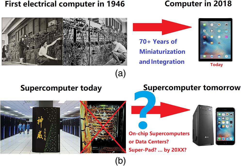
    Fig. 1. Comparison of (a) first electrical computer with (b) today’s supercomputer. The similarity in volume and power consumption as well as the dramatic size reduction and improvement in computation power of the electrical computers over the last 70 years naturally raise an interesting question: would we ever be able to achieve similar volume reduction of today’s supercomputers through miniaturization and integration?
    (a) Schematic of a laser-based optical interconnect in a present-day supercomputer based on VCSELs and optical fiber and (b) future on-chip interconnect based on a nanolaser array and a waveguide array.
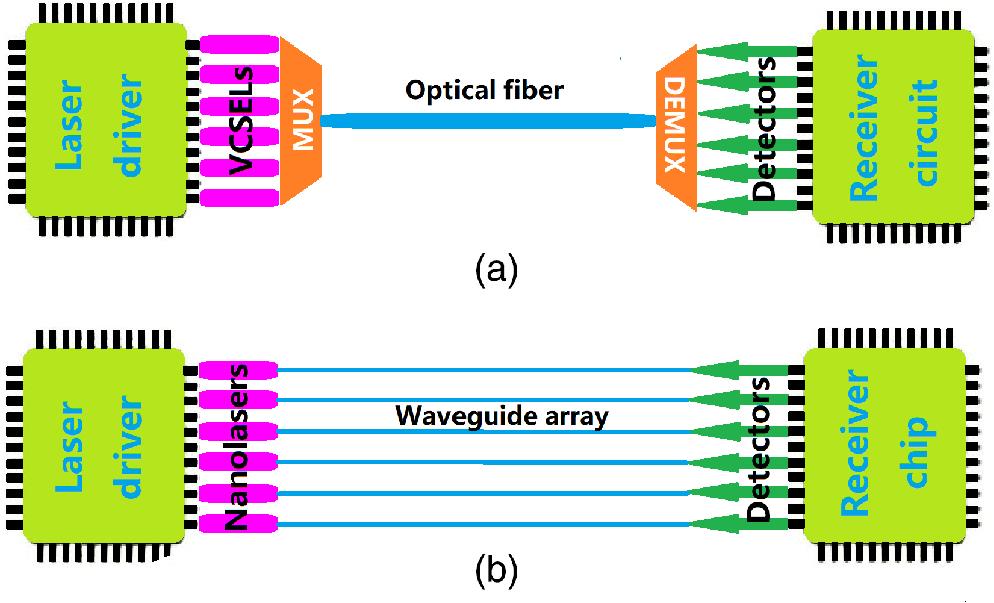
    Fig. 2. (a) Schematic of a laser-based optical interconnect in a present-day supercomputer based on VCSELs and optical fiber and (b) future on-chip interconnect based on a nanolaser array and a waveguide array.
    Relationship between energy efficiency (EDR, in fJ/bit) and modulation bandwidth for various values of diameter for a cylindrical laser (adapted from Ref. 22).
    Fig. 3. Relationship between energy efficiency (EDR, in fJ/bit) and modulation bandwidth for various values of diameter for a cylindrical laser (adapted from Ref. 22).
    Device volume normalized by the wavelength cubed for several types of semiconductor lasers: EEL, edge emitting lasers; MD, microdisk; P-laser, plasmonic lasers. Symbols represent typical values for these lasers; colored bars indicate the ranges of values found in the literature. Red marks along the x axis indicate the years when the type of laser was first experimentally demonstrated. The yellow bar is extended intentionally downward beyond the data symbols to indicate the potential for further size reduction for plasmonic laser and spaser.
    Fig. 4. Device volume normalized by the wavelength cubed for several types of semiconductor lasers: EEL, edge emitting lasers; MD, microdisk; P-laser, plasmonic lasers. Symbols represent typical values for these lasers; colored bars indicate the ranges of values found in the literature. Red marks along the x axis indicate the years when the type of laser was first experimentally demonstrated. The yellow bar is extended intentionally downward beyond the data symbols to indicate the potential for further size reduction for plasmonic laser and spaser.
    Comparison of a dielectric cavity and a metallic cavity. (a) The dependence of the cavity Q factor on its diameter for two cavities: a pure dielectric cavity and a dielectric cylinder with a metal shell (adapted from Ref. 84). (b) Laser performance comparison of a semiconductor pillar cavity [denoted with (D)] and a semiconductor pillar cavity with metal shell [denoted with (M)] (from the supporting information of Ref. 22): the laser output power (P) and temperature (T) are shown.
    Fig. 5. Comparison of a dielectric cavity and a metallic cavity. (a) The dependence of the cavity Q factor on its diameter for two cavities: a pure dielectric cavity and a dielectric cylinder with a metal shell (adapted from Ref. 84). (b) Laser performance comparison of a semiconductor pillar cavity [denoted with (D)] and a semiconductor pillar cavity with metal shell [denoted with (M)] (from the supporting information of Ref. 22): the laser output power (P) and temperature (T) are shown.
    Contributions of the photonic and electronic densities of states to the size reduction and energy efficiency of semiconductor nanolasers.
    Fig. 6. Contributions of the photonic and electronic densities of states to the size reduction and energy efficiency of semiconductor nanolasers.
    Cun-Zheng Ning. Semiconductor nanolasers and the size-energy-efficiency challenge: a review[J]. Advanced Photonics, 2019, 1(1): 014002
    Download Citation