Abstract
Semiconductor lasers, an important subfield of semiconductor photonics, have fundamentally changed many aspects of our lives and enabled many technologies since their creation in the 1960s. As in other semiconductor-based fields, such as microelectronics, miniaturization has been a constant theme, with nanolasers being an important frontier of research over the last decade. We review the progress, existing issues, and future prospects of nanolasers, especially in relation to their potential application in chip-scale optical interconnects. One of the important challenges in this application is minimizing the size and energy consumption of nanolasers. We begin with the application background of this challenge and then compare basic features of various semiconductor lasers. We present existing issues with nanolasers and discuss potential solutions to meet the size and energy-efficiency challenge. Our discussions cover a broad range of miniaturized lasers, including plasmonic nanolasers and lasers with two-dimensional monolayer gain materials, with focus on near-infrared wavelengths.1 Introduction
The research field of semiconductor lasers is at the very core of the larger field of semiconductor photonics (also known as optoelectronics). This is a field encompassing both fundamental science and a wide range of important technologies. From the scientific perspective, light–semiconductor interaction plays a foundational role in understanding semiconductors as gain media. The development of semiconductor lasers since the early 1960s has played an important role in our understanding of the basic optical properties of semiconductors and has revealed a wealth of important physical phenomena over the last five decades or so. From a technological perspective, semiconductor lasers have fundamentally altered the technology landscape and contributed greatly to our modern lifestyle—from miniature semiconductor lasers that are ubiquitous in many tech gadgets (such as CD/DVD players, sensors in our smartphones, and bar-code scanners) to the lasers that serve as workhorses within the modern communication systems that drive our internet, supercomputers, and data centers. As we stand at the beginning of the second half-century of semiconductor lasers, it is important to review the frontiers of the field, to foresee and analyze any potential challenges, and to develop strategies to meet such challenges. As with the larger field of semiconductor photonics, semiconductor laser research faces three major challenges: device size and energy efficiency, wavelength or bandgap diversity, and system integration. These challenges are explored in the following sections.
1.1 Device Size and Energy-Efficiency Challenge
The sizes of photonic devices are generally limited by the wavelengths involved. Thus, it becomes an important challenge to overcome wavelength limits or diffraction limits. The important questions to ask are whether, how, and to what degree we can break the diffraction limit to create ever smaller and better optoelectronic devices such as lasers. An important related issue is the energy efficiency of photonic devices (such as lasers, modulators, and switches) when used for information transmission,1 in terms of joule per bit of information transmitted. These questions and their related challenges are important for realizing future integrated nanophotonic on-chip circuits.
1.2 Wavelength or Bandgap Diversity Challenge
All semiconductor photonic devices, including lasers, are based on light–semiconductor interaction involving either absorption or emission of photons by semiconductors. Important spectral response (emission, refraction, or absorption) of any semiconductor is ultimately determined by its electronic bandgap and bandstructure. Many applications require (or can significantly benefit from) bandgaps that can be controllably tuned in a wide range, allowing bandgap diversity or flexibility, preferably on a single substrate or monolithically.2 However, our ability to achieve the required diversity of bandgap is rather limited, primarily because of the lattice-matching required in typical planar epitaxial growth of high-quality semiconductors. Such lack of ability to produce the requisite bandgaps severely impedes technological progress in many applications, including displays, solid-state lighting, solar cells, detectors, and widely tunable lasers. Nanoscale semiconductors, such as nanowires,2–4 perovskite platelets,5 and quantum dots, offer many potential benefits and have enabled many exciting developments, such as widely tunable emission in the entire visible spectrum, or white lasers from a single substrate, or a single monolithic semiconductor. Such nanomaterials must be fully and systematically explored to develop more mature devices.
Sign up for Advanced Photonics TOC. Get the latest issue of Advanced Photonics delivered right to you!Sign up now
1.3 Integration Challenge
A well-recognized long-term challenge is the achievement of integrated photonics on a silicon platform. While most passive devices can be fabricated directly on an Si platform, light sources are still almost exclusively made of III-V materials. Thus, heterogeneous integration of III-V-based lasers, or gain materials onto Si-waveguides, has become a prevailing approach.6–9 Although mismatch of the material properties between typical III-V semiconductors and Si has prevented direct growth of high quality III-V semiconductor films on Si using the typical planar growth techniques, recent work in nanomaterials has shown promise for direct monolithic growth of various nanomaterials on Si, such as III-V quantum dots10–12 and nanowires.13–21 Such a nanomaterials approach could be widely applied in the long run. However, achieving efficient lasers on a silicon substrate remains an important challenge.
This paper presents an analysis and summary of the aforementioned challenges in semiconductor laser research, with focus on one of the frontiers of the field, namely, semiconductor nanolasers. We focus on the long-term issues and fundamental challenges that are likely to remain unresolved for the foreseeable future, and those that will impact the field in profound ways. In particular, the size-energy-efficiency challenge is emphasized because of its importance and potential impact on the other two challenges and on the entire field of semiconductor photonics. In the following sections, the background of the size-energy-efficiency challenge is introduced, and the relevant progress made in the last decade or so is highlighted. The potential and shortcomings of each approach are analyzed. Finally, we present future perspectives in the resolution of these challenges and the possible impact on the field of semiconductor lasers and photonics.
2 Size and Energy-Efficiency Challenge
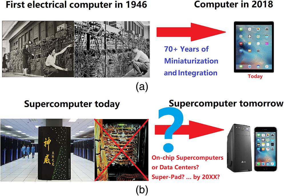
To motivate the need for ever-smaller lasers, we recall one of the greatest technological revolutions of our times, namely, the computer revolution. The transformation of the first electrical computers to the present-day laptop or iPad [see Fig. 1(a)] represents the best of miniaturization and integration in electronics through Moore’s law. There are certain “superficial” similarities between the first electrical computers and the present-day supercomputers or data center server computers [see Fig. 1(b)], in terms of size (floor space occupied), overall power consumption, and even cables (albeit electrical cables versus optical fiber cables). The superficial similarities raise an obvious question: could the current supercomputers or data center servers be made much more compact (and to what degree) through miniaturization and integration in a way similar to that achieved in transforming the first electrical computer in to present-day PCs or iPads? Presently, the answer to this question is not completely clear, including when, in what form, or to what degree such size/volume reduction is possible. However, it is certain that miniaturization and integration of all types of photonic devices are indispensable. And the large number and volumes of optical cables must be largely replaced, similar to the replacement of electrical cables and wires that connected all the electrical devices in the original electrical computers through transistor-based integrated circuits. To achieve such replacement, optical communications (interconnects) need to be conducted largely on-chip or on-board, as schematically shown in Fig. 2; such replacement involves a mixed optical and electronic (OE) integration. Therefore, instead of transistors, a large variety of optical elements (devices), such as modulators, beam splitters, amplifiers, and light sources (lasers), must be developed for this second round of integration, or OE integration. It is hoped that this second integration would also lead to the second computer revolution, i.e., miniaturization of supercomputers and data center servers.

Figure 1.Comparison of (a) first electrical computer with (b) today’s supercomputer. The similarity in volume and power consumption as well as the dramatic size reduction and improvement in computation power of the electrical computers over the last 70 years naturally raise an interesting question: would we ever be able to achieve similar volume reduction of today’s supercomputers through miniaturization and integration?
Figure 2.(a) Schematic of a laser-based optical interconnect in a present-day supercomputer based on VCSELs and optical fiber and (b) future on-chip interconnect based on a nanolaser array and a waveguide array.
For such OE integration, it is important to significantly reduce the sizes of the optical devices and reduce the size mismatch between optical devices and electronic devices. Currently, typical optical devices, such as lasers, are two- to three-orders of magnitude larger than electrical devices. It is typically argued that the size mismatch between photonic and electronic devices is due to the much longer wavelengths of photons than electrons. Although it is true that wavelengths of photons are ultimately limited to the sizes of photonic devices, the wavelengths are presently not the limiting factor. Far more important at this stage is the “functionality” determined size limit. For example, the size of a modulator is determined by the length required to achieve a given amount of phase change (functionality length limit); this length is typically much larger than the wavelength of laser light. The functionality limit in a semiconductor laser is the gain length required to overcome the threshold and achieve lasing.2 Presently, the functionality limit is much larger than the wavelengths involved in typical photonic devices; thus, reducing this functionality limit is of highest priority to address size miniaturization.
Miniaturization of photonic devices is not merely required for the sake of size parity with electronic devices. Such miniaturization is more importantly related to energy efficiency, or the amount of energy an optical device consumes for each bit of information it transmits, also known as the energy-data rate (EDR), often expressed in the unit of femtojoule per bit.2,22 According to various system level analyses, photonic devices used for on-chip communications require the energy efficiency to be better than 10 fJ/bit and less than 1 fJ/bit in the near future, to be competitive with electronic interconnects.2 Presently, semiconductor lasers consume typically more than 1 pJ/bit (or milliwatt per Gbs). According to IBM’s estimate,23 exascale computers would require 800 million optical channels of 25 Gbs each for interconnects, representing a total power consumption of 20 MW for optical interconnects alone if an energy efficiency of 1 pJ/bit is assumed. Such a level of power consumption is obviously too high to tolerate. Thus, it is important to reduce the energy consumption of an optical transmitter, i.e., a semiconductor laser in the case of a directly modulated transmitter.
There is a close relationship between size, speed, and energy efficiency, as we demonstrated recently.22 A special case of this study22 is shown in Fig. 3 for a semiconductor laser of a cylindrical shape with diameter varying from microns to hundreds of nanometers. We see that device sizes on the orders of a few hundred nanometers in diameter are required for energy efficiency on the order of 1 fJ/bit. This analysis clearly demonstrates why nanolasers are required for such applications. Figure 3 also shows that there is an optimum modulation bandwidth corresponding to the smallest EDR for each device size. The initial decrease of the EDR is a result of increasing bandwidth with a relatively small increase of energy consumption. The second stage increase of EDR is primarily caused by the significant energy increase due to increased driving current beyond CW current. As lasers become smaller, the minimum of EDR moves to higher bandwidth via the Purcell effects with smaller lasers. Both for reducing the size mismatch with electronic devices and for improving the energy efficiency, we need photonic devices (especially lasers) with sizes as small as hundreds of nanometers in diameter. Presently, it is not entirely clear how to make lasers of such small sizes without the use of plasmonic or photonic crystal structures. Thus, realizing lasers of small size and high energy efficiency is the major challenge faced by the semiconductor photonics community. Note that, in general, smaller devices, higher bandwidth, and more efficient operation are all mutually related and compatible, as indicated by the orange arrow pointing toward the lower right of Fig. 3, indicating the future direction of nanolaser research. For EDR below 1 fJ/bit, i.e., in the attojoule per bit range, Fig. 3 indicates that the devices need be on the order of 100 nm. This requirement clearly illustrates the importance of nanolasers and represents a significant challenge for laser design and fabrication. An additional trade-off with the miniaturization is the increased bit-error rate due to the reduction of total photon number.22
Figure 3.Relationship between energy efficiency (EDR, in fJ/bit) and modulation bandwidth for various values of diameter for a cylindrical laser (adapted from Ref. 22).
3 Miniaturization of Semiconductor Lasers
Semiconductor lasers are the smallest and most energy efficient lasers among all types of lasers. They are best suited for applications involving on-chip or onboard integration because of their compact sizes and energy efficiency, and the possibility of operation under the convenient electrical bias. Such intrinsic advantages are, however, not sufficient to meet the much more stringent requirements of future optoelectronic-integrated chips. For these and many other reasons, constant size reduction has been one of the most recognizable features in the development of optoelectronics via constant inventions of paradigms of laser cavities over the past five decades. Figure 4 shows typical ranges of the volumes of various semiconductor lasers along with the year of the first demonstration of each type of laser. We see over five order-of-magnitude reductions in the volume of semiconductor lasers have been achieved over the last five decades since the demonstration of the first semiconductor lasers, via continuous innovations in design and improvements of fabrication techniques. Despite having the best power efficiency from electrical to optical watts, typical edge-emitting lasers (EELs) are too large for on-chip interconnects with high EDR. Typical EELs have dimensions in the range of several in width, hundreds of in length, and a total device volume from 100 to 1000 times the wavelength cubed (see Fig. 4). Some of the other potential candidates are described in the following sections.
Figure 4.Device volume normalized by the wavelength cubed for several types of semiconductor lasers: EEL, edge emitting lasers; MD, microdisk; P-laser, plasmonic lasers. Symbols represent typical values for these lasers; colored bars indicate the ranges of values found in the literature. Red marks along the axis indicate the years when the type of laser was first experimentally demonstrated. The yellow bar is extended intentionally downward beyond the data symbols to indicate the potential for further size reduction for plasmonic laser and spaser.
3.1 Vertical Cavity Surface Emitting Lasers
VCSELs, which are one of the most important types of microsize lasers, were invented24 many years after the initial demonstration of conventional EELs. VCSELs offer a size reduction of at least an order of magnitude in total device volume compared to EELs (see Fig. 4). Currently, VCSELs are one of the most energy-efficient types of lasers that are deployed in practical applications. Even though VCSELs as energy efficient as 50 fJ/bit have been demonstrated in research laboratories,25–27 those deployed in practice are much less energy-efficient. Typical VCSELs have diameters of to with a total DBR thickness of to , resulting in a total device volume of 10 to 100 times the wavelength cubed, although the modal volumes are much smaller. Further significant reduction in sizes and energy usage are difficult to achieve because of the poor heat dissipation through thick DBR mirrors and the poor lateral confinement of the VCSEL structures. Thus, it is very difficult for VCSELs to meet the long-term requirements of the size and energy-efficiency challenge for on-chip applications, despite great improvements in recent years.27
3.2 Microdisk Lasers
Microdisk lasers were initially developed28–30 in attempts to miniaturize semiconductor lasers for integrated photonics applications using a free-standing piece of semiconductor based on whispering-galley modes due to the high contrast of refractive indices between semiconductor and air. Such index contrast provides the strongest mode confinement realistically possible without the use of metals or thick DBRs. The unique structures allowed much smaller lasers than possible at the time. The initial devices had diameters between and with a thickness of approximately one micron, resulting in a total device volume of several times the wavelength cubed. Recent work30 combining the photonic crystal (PC) structure with a microdisk allowed a total device volume of only a small fraction of a wavelength cubed, one of the smallest total volumes achieved (see Fig. 4). Significant progress has also been made recently in demonstrating micro- or nano-disk lasers using perovskites.5,31 Even though perovskites show remarkable optoelectronic properties and may find many interesting applications elsewhere, their use for on-chip interconnects is hindered by several issues such as incompatibility with traditional microfabrication and the lack of perovskites that emit at near-infrared communication wavelengths (e.g., ).
3.3 Photonic Crystal Lasers
Photonic crystal lasers30,32–38 are promising candidates for use in energy-efficient applications because they have very small volumes of optical modes and represent a type of laser based on a very fruitful wave-analogy between electrons and photons.39,40 These lasers can have very low thresholds as a result. Recently, direct modulation at 5.5 GHz at room temperature via optical pumping has been demonstrated.33,37 The energy efficiency was estimated to be 13 fJ, with one of the lowest threshold pumping powers, estimated at . Although the defect modes that define the cavity in a PC laser can be extremely small, the overall sizes of PC structures can have diameter or side length on the order of , resulting in a total device volume that ranges from several to 100 times the wavelength cubed, as shown in Fig. 4. Such lasers are of great importance both for studying basic quantum optics of nanolasers and for potential use in integrated photonic applications because of the ability to achieve unprecedented tight three-dimensional (3-D) mode confinement. The total device sizes including the large periodic dielectric structures are very large, however.
3.4 Nanowire or Nanopillar Lasers
Semiconductor nanowires or nanopillars in air provide one of the best semiconductor optical cavities via the large index contrast (similar to that of microdisk lasers). As with the microdisk lasers, the mode confinement is much better than in typical double-heterostructures, with the possibility of achieving a confinement factor of . Such nanowires with the two ends exposed to air provide a unique structure both for high-reflective laser cavity and a gain medium at the same time, an ideal combination for laser miniaturization.41 After the initial wave of laser demonstration in the UV and visible wavelength regime,42–44 the first near IR lasing45 was demonstrated using a single GaSb nanowire at the telecom wavelengths. Recently, several realizations of lasing were demonstrated in the short wavelength NIR regime.13,46,47 To date, almost all of these demonstrations of nanowire lasing were achieved under optical pumping, with only one exception.44 The ranges of volumes of nanowire lasers are currently comparable to those of microdisk lasers and PC lasers (see Fig. 4), with the total size as small as twice the wavelength cubed in the IR range.45 However, further miniaturization of nanowires is possible. One additional advantage of nanowire lasers is the combined material and bandgap flexibility,2 which allows realization of lasers at wavelengths that are difficult to achieve using either the microdisk approach or the PC approach. Many recent review articles3,4,48–53 are available on nanowires and the nanowire-based lasers.
3.5 Two-Dimensional Material Nanolasers
With the reduction of laser cavity size or volume, the cavity quality factor decreases. This decrease in cavity quality factor occurs for both pure dielectric cavities and metallic or plasmonic (see Sec. 4) cavities, albeit according to different scaling laws.54 Therefore, it is important to constantly search for better gain materials that provide high optical gain within a small volume. In this regard, the newly emerging 2-D materials, such as transition metal dichalcogenides (TMDCs), show great promise. One of the key features of these 2-D materials is the extremely large exciton binding energy (generally one or two orders of magnitude larger than conventional semiconductors). This feature allows 2-D-based materials to provide high optical gain at room temperature or higher through exciton-related emissions before the Mott transition, rather than through the typical quasifree electron-hole plasma used in conventional semiconductor lasers. The possibility of excitonic gain is extremely appealing for low power applications since it requires much lower levels of carrier density than electron-hole plasma. Even for plasma gain, strong excitonic enhancement of optical gain will also be beneficial. Another advantage is the monolayer thickness of the 2-D materials, thereby providing the necessary flexibility for integration with different substrates, especially Si substrates, to address the integration challenge. The much larger tolerance to strain and other mismatched mechanical properties could be very valuable compared to conventional III-V materials for Si integration. The monolayer also provides the thinnest gain materials with an overall small volume, important for low input energy. Lasing demonstrations using 2-D materials have been reported in a microdisk cavity,55 and in 2-D56 and 1-D57 PC cavities; such demonstrations have been achieved at low temperatures55,56 and at room temperature for IR wavelengths that are Si transparent.57 Strong and weak coupling to cavity modes58–60 has also been studied. As mentioned, the monolayer thickness combined with a nanoscale cavity57 leads to a small overall laser with a mode volume smaller than and a gain medium volume . All these characteristic parameters are quite attractive for energy efficient applications.
4 Plasmonic Nanolasers and Spasers
4.1 Progress Overview
Plasmonic lasers or spasers61–65 are the newest member of the laser family; such lasers can realize the smallest sizes of any lasers and thus can be potentially energy-efficient lasers when small size is essential. Plasmonic lasers utilize the coupling between photons and plasmon excitation at metal–dielectric interfaces to confine photons to the smallest possible spatial volumes. The pioneering proposal of spasers by Bergman and Stockman61 was to create a stimulated plasmonic source; it soon became clear that the unavoidable far-field coupling could be utilized to allow the stimulated plasmonic source to emit coherent laser light to serve as an ultrasmall laser. Plasmon polariton propagation was earlier studied for the purpose of prolonging the propagation length.64,66,67 A plasmonic nanolaser design with the explicit purpose of achieving a miniaturized laser was proposed in the form of a semiconductor core in a silver metal shell.62 The design and simulation showed that, despite the expected high plasmonic loss, the high level of optical gain in the semiconductor core could overcome the associated high threshold loss. Afterward, a similar core–shell-structured laser was soon demonstrated using a traditional top-down lithographical fabrication based on InP, demonstrating the first metallic cavity core–shell nanolaser.68 Although this demonstration was impressive in terms of fabrication quality down to such a small size, the operation modes were not plasmonic, but conventional dielectric modes.
One of the first demonstrations of plasmonic mode lasing63 was reported soon afterward; such lasing, which is closer to the original proposal,62 involved the use of an InP/InGaP/InP core and silver shell, with the core having a rectangular cross section etched from an InP-InGaAs wafer with thickness varying between 80 and 340 nm. The device operated in the so-called plasmonic-gap mode, with a semiconductor core as thin as 80–90 nm. The entire optical thickness of the device, including the SiN insulating layer and the metal penetration, is , which is much smaller than the half-wavelength (670 nm) of the operating laser emission. This work represents the first laser with at least one dimension below the “diffraction limit,” a result that is impossible to achieve using a pure dielectric mode. Simultaneously, other forms of spaser or plasmonic nanolaser operation were demonstrated using an Au core coated by a dye-doped dielectric outer shell,69 or a CdSe nanowire placed on a silver screen separated by a thin dielectric film.65 Note that both Refs. 63 and 65 are based on the same plasmonic gap modes, even though the gap in Ref. 65 is much smaller. After these initial demonstrations of plasmonic nanolasers or spasers, the field has flourished, with a wide array of designs reported,70–82 for which the plasmonic or metallic structures feature prominently as the mechanism for light confinement. Such a fundamental change, from the traditional dielectric/semiconductor cavities to metallic or plasmonic cavities, represents a potential paradigm shift in laser cavity design. These plasmonic cavity designs include metallic co-axial structures,71,81 metallic nanopan structures,80 metallic structures combined with VCSELs, metallic trench FP cavity, and metal-grating DFB structures.74,75 Although plasmonic laser operation under optical pumping dominates the research literature, electrical injection devices54,63,68,77,83,84 have been studied from the very beginning, based on semiconductor wafer structures that are more compatible with the standard III-V fabrication technologies. Room temperature operation of metallic cavity lasers under electrical injection has also been demonstrated,77,83 indicating potential applicability of such lasers for practical applications. Linewidth of plasmonic nanolaser is an interesting issue and has been studied recently.85 Many good review articles in the literature provide more complete perspectives on plasmonic nanolasers from the perspectives of various groups.49,54,84,86–91
4.2 Benefits of Plasmonic Nanolasers
Several important advantages of plasmonic nanolasers that are relevant to size and energy efficiency are worth mentioning here. One advantage is the size or volume. When comparing the sizes or volumes of various lasers, it is important to note that there are three types of volume that are relevant: the volume of the active region, the modal volume, and the total volume of devices. The volume of the active region determines the total number of electron-hole pairs that need to be injected. For a given transparency carrier density, the smaller the volume of the active region is, the smaller the threshold current, and thus, the smaller the total electrical energy input (I-V product). For low energy operation, a small active region is preferred. The small modal volume often results in a large confinement factor if the optical modes enclose the active region. A large confinement factor corresponds to a large modal gain. The total device volume is often limited by the precious availability of real estate on chip for integrated photonics applications and is also related to the heat dissipation efficiency. Thus, all three volumes must be small for lasers to be used as on-chip light sources. An efficient small laser will preferably have all three volumes as small and as closely equal as possible. Plasmonic lasers can be designed to have the smallest values of all three volumes among all the proposed types of nanolaser.92 For example, PC lasers, which have small modal volumes, often have large volumes of the active region and large total device volumes. Currently, most of the plasmonic lasers demonstrated have not been miniaturized in all three dimensions and can be further optimized to further reduce sizes in one or two more dimensions.92
Because energy efficiency is defined as the energy consumed per bit of information transmitted, energy efficiency benefits greatly from high-speed operation. Purcell enhancement (see Fig. 6) in plasmonic devices is the strongest among all the proposed structures. Such enhancement leads to higher laser modulation speed. Extremely high speed of operation was predicted (up to THz) theoretically.90,93 Ultrafast experiments indicate enhanced gain switch and recover times.82 The realistically achievable speed is, however, much lower.22,93–96 Modulation at hundreds of GHz appears to be realizable;22,95 such modulation speed is already much higher than that of typical semiconductor lasers. Significant improvement in modulation speed is expected with further improvements in plasmonic laser design and fabrication.
Low lasing threshold is generally desired for low power consumption. This might lead people to believe that plasmonic or metallic cavity lasers are unsuited for energy-efficient applications. However, low threshold alone does not always translate into high energy efficiency. Many conventional lasers, such as VCSELs, have extremely low thresholds; however, their energy efficiency is too low for future integrated photonics applications, as mentioned earlier. Figure 3 shows that small sizes are important for low energy operation. However, when we demand both small size and low threshold, the situation is somewhat more complicated. Figure 5(b) shows a comparison of the -factor for modes with wavelength of for two modal laser cavities:84 dielectric disk cavities with and without metallic shell. Clearly, a dielectric cavity without a metal shell displays a much more rapid decrease of with the decrease of diameter than that with a metal shell; this difference is caused by the rapid increase of far-field radiative loss with a decrease in diameter, as mode confinement deteriorates. In contrast, the cavity with metal shell shows a much slower decrease compared to the cavity without a metal shell. The two curves cross over near 1000 nm, indicating an overall benefit in using a metallic shell cavity for smaller (submicron) devices, due to reduction of far-field radiative loss, despite the large metal loss. A trade-off clearly exists between far-field radiative loss and internal absorption loss. For a smaller device, the metallic cavity is an overall better choice for lower threshold and higher energy efficiency (Fig. 3), contrary to the intuitive arguments.
Figure 5.Comparison of a dielectric cavity and a metallic cavity. (a) The dependence of the cavity factor on its diameter for two cavities: a pure dielectric cavity and a dielectric cylinder with a metal shell (adapted from Ref. 84). (b) Laser performance comparison of a semiconductor pillar cavity [denoted with (D)] and a semiconductor pillar cavity with metal shell [denoted with (M)] (from the supporting information of Ref. 22): the laser output power (P) and temperature (T) are shown.
Heat dissipation is another important factor for high-density on-chip integration and thus must be considered when comparing various lasers. Many of the other proposed laser miniaturization solutions suffer from poor heat dissipation, such as nanowire lasers, PC lasers, and microdisk lasers, because of the long or poor heat conduction channels involved in these lasers. For example, the airgaps involved in most of the PC lasers prevent a more efficient downward heat dissipation to the substrate. Plasmonic lasers provide potential advantages in this respect via the close proximity of metal shell to active region22,63 and much improved heat conduction by the metal. These advantages are illustrated in Fig. 5(b). As discussed in detail in Ref. 22 (see Supporting Information there), two semiconductor lasers of cylindrical pillar shape with and without the metallic shell were considered in numerical simulation. The two lasers have the same diameter of 920 nm. The -factor considered is 280 and 421 for nanolaser with and without metal shell, respectively. Note that intentional choice of somewhat larger size favors the nanolaser without metal shell because it has higher and thus lower threshold. As seen in Fig. 5(b), the laser without the metal shell indeed turns on at lower pumping. However, at higher pumping levels, the poor heat dissipation leads to significant heating, with a temperature increase as high as 100 K above the substrate temperature. Overheating eventually leads to device shut off. In contrast, the laser with a metal shell shows only a modest temperature increase; as a result, it has much higher output power at high pumping levels. Ability to operate at high driving current is indeed an important advantage of plasmonic lasers compared to conventional semiconductor lasers.
Another counterintuitive result is the plasmonic enhancement of optical gain due to an unusual feature of confinement factor near plasmonic resonance,97 resulting in slowing down of energy propagation. This slow energy propagation leads to a giant enhancement of optical gain,98 leading to much higher optical gain than material gain. Such giant optical gain could lead to a significant decrease of laser threshold. However, the slowed-down energy propagation may affect the modulation speed when extreme high speed is desired. A detailed optimization of the trade-off between low threshold and high modulation speed is required to achieve optimal performance.
5 Issues and Perspectives
Although VCSELs are deployed widely in many applications, including optical interconnects in supercomputers and datacenters, their applications for on-chip interconnects in the long run are hindered by the relatively large volume, which limits the energy efficiency to above tens to hundreds of fJ/bit. Significant reduction below this level is not likely. Furthermore, thick DBRs in VCSELs result in very high profile and inefficient heat dissipation, a significant disadvantage for on-chip integration.
To date, microdisk lasers are among the smallest lasers, as shown in Fig. 3; however, without incorporation of mode confinement mechanisms (such as plasmonic confinement), they have nearly reached their size limit. Furthermore, such lasers are often pumped optically; operation under electrical injection remains a significant challenge to achieve. Microdisks often must be suspended or supported by a smaller stem, leading to poor heat dissipation and mechanical stability. Significant research is required to fabricate electrical injection disk lasers. Research on high-speed modulation and energy efficiency remains to be performed for microdisk lasers.
PC lasers are among the best developed nanoscale lasers to date, with high-speed modulation, reasonable energy efficiency, and electrical injection pumping demonstrated; however, their current power efficiency is well below that of typical EELs or VCSELs. Significant research is still required to improve electrical injection efficiency and device wall plug efficiency. Similar to microdisk lasers, PCs typically involve under-etching to increase mode confinement vertical to the PC plane, making heat dissipation inefficient and the mechanical stability quite poor. In addition, the total sizes of typical PC lasers are still on the order of 10s of microns, even though the modal volumes are much smaller. One major advantage of PC lasers compared to plasmonic nanolasers is the low threshold. PC lasers are quite strong candidates for use as on-chip lasers for interconnects, especially where the large total volume can be accepted.
There is still significant room for size reduction of semiconductor nanowire or nanopillar lasers. The great advantages of such lasers are their 1-D morphology and high index contrast (allowing them to serve as natural waveguides and cavities) and their material flexibility in energy bandgaps (via the larger tolerance to lattice mismatch). However, nanowire lasers are not yet mature enough for systematic examination in terms of high-speed modulation and low-power applications. Electrical injection remains difficult based on the bottom-up manufacturing approach. The full potential of nanowire lasers is difficult to estimate accurately, leaving more research opportunities for device engineers.
Plasmonic nanolasers promise to provide high-speed operation. However, systematic experimental work on high-speed modulation is lacking. Demonstration of electrical injection plasmonic nanolasers remains a significant challenge, especially at high temperature. The demonstrated electrical injection operation at higher operation temperature is usually based on dielectric modes. Innovative designs of plasmonic nanolasers are required that take full consideration of low loss, high injection efficiency, high speed, and low energy consumption.
Most of the discussions of this article have focused on the cavity or mode confinement mechanism. In the long run, the ultimate solutions to the size-energy-efficiency challenge require design and fabrication from both the photon aspect (i.e., cavity design or mode confinement) and the charge carrier aspect (i.e., gain medium). As shown in Fig. 6, optoelectronic devices such as lasers require a gain medium with an efficient radiative process, the efficiency of which is determined by two densities of states: the density of photonic states and the density of electronic states. These two densities of states must be considered simultaneously. The direct consequence of cavity size reduction is a Purcell-enhanced radiative process, which uses photons in an increasingly efficient manner as the size of the devices decreases and the Purcell enhancement increases. From the electronic aspect, the reduction of dimensionality of gain materials from bulk, quantum wells, and quantum wires, to quantum dots makes the population of electrons and holes in the energy space more efficient by putting them where they will be used for emission into cavity modes. Only when we use both photons and electrons/holes in their respective spectral domains more efficiently (or economically) can we hope to have the most efficient photon–semiconductor interaction and ultimately produce the smallest and most efficient optoelectronic devices and nanolasers. There remains room for further optimization from both sides to improve device efficiency. In this regard, quantum dot materials and 2-D TMDC materials are of great long-term interest, due to their potential for providing the smallest volume of gain materials. Operation of 2-D-materials-based nanolasers under electrical injection has not been demonstrated and appears to be challenging. Two-dimensional materials such as TMDCs as optical gain materials are largely unexplored with a few very recent exceptions,99–102 and a great deal of research effort is required in the near future to fully assess their suitability as optical gain materials to meet the size-energy-efficiency challenge.
Figure 6.Contributions of the photonic and electronic densities of states to the size reduction and energy efficiency of semiconductor nanolasers.
References
[1] D. A. B. Miller. Device requirements for optical interconnects to silicon chips. Proc. IEEE, 97, 1166-1185(2009).
[2] C. Z. Ning, L. T. Dou, P. D. Yang. Nanoscale bandgap engineering: semiconductor alloy nanomaterials with widely tunable compositions. Nat. Rev. Mater., 2, 17070(2017).
[3] C. Z. Ning. Semiconductor nanolasers (Tutorial). Phys. Status Solidi B, 247, 774-788(2010).
[4] J. J. Coleman, C. Z. Ning, A. C. Bryce, C. Jagadish. Semiconductor nanowire lasers. Semiconductors and Semimetals, 86, 455-486(2012).
[5] Q. Zhang et al. High quality whispering gallery mode lasing from cesium lead halide perovskite nanoplatelets. Adv. Funct. Mater., 26, 6238-6245(2016).
[6] D. Liang, J. E. Bowers. Recent progress in lasers on silicon. Nat. Photonics, 4, 511-517(2010).
[7] K. Ohashi et al. On-chip optical interconnect. Proc. IEEE, 97, 1186-1198(2009).
[8] Z. Wang et al. Novel light source integration approaches for silicon photonics. Laser Photonics Rev., 11, 1700063(2017).
[9] D. Liang et al. Heterogeneous silicon light sources for datacom applications. Opt. Fiber Technol., 44, 43-52(2018).
[10] A. Y. Liu et al. High performance continuous wave 1.3 μm quantum dot lasers on silicon. Appl. Phys. Lett., 104, 041104(2014). https://doi.org/10.1063/1.4863223
[11] T. Wang et al. 1.3-μm InAs/GaAs quantum-dot lasers monolithically grown on Si substrates. Opt. Express, 19, 11381-11386(2011). https://doi.org/10.1364/OE.19.011381
[12] S. Chen et al. Electrically pumped long lifetime continuous-wave III-V quantum-dot lasers directly grown on silicon substrates. Nat. Photonics, 10, 307-311(2016).
[13] R. Chen et al. Nanolasers grown on silicon. Nat. Photonics, 5, 170-175(2011).
[14] A. T. Martensson et al. Epitaxial III-V nanowires on silicon. Nano Lett., 4, 1987-1990(2004).
[15] K. Tomioka, M. Yoshimura, T. Fukui. A III–V nanowire channel on silicon for high-performance vertical transistors. Nature, 488, 189-192(2012).
[16] M. Borg et al. Vertical III-V nanowire device integration on Si(100). Nano Lett., 14, 1914-1920(2014).
[17] Y. Cohin et al. Growth of vertical GaAs nanowires on an amorphous substrate via a fiber-textured Si platform. Nano Lett., 13, 2743-2747(2013).
[18] B. Mayer et al. Monolithically integrated high-β nanowire lasers on silicon. Nano Lett., 16, 152-156(2016).
[19] F. Schuster et al. Site-controlled growth of monolithic InGaAs/InP quantum well nanopillar lasers on silicon. Nano Lett., 17, 2697-2702(2017).
[20] H. Kim et al. Monolithically integrated InGaAs nanowires on 3D structured silicon-on-insulator as a new platform for full optical links. Nano Lett., 16, 1833-1839(2016).
[21] H. T. Nguyen et al. p-Type modulation doped InGaN/GaN dot-in-a-wire white-light-emitting diodes monolithically grown on Si(111). Nano Lett., 11, 1919-1924(2011).
[22] K. Ding et al. Modulation bandwidth and energy efficiency of metallic cavity semiconductor nanolasers with inclusion of noise effects. Laser Photonics Rev., 9, 488-497(2015).
[23] A. Benner. Optical interconnect opportunities in supercomputers and high end computing, OTu2B.4(2012).
[24] H. Soda et al. GaInAsP/InP surface emitting injection lasers. Jpn. J. Appl. Phys., 18, 2329-2330(1979).
[25] P. Moser et al. 56 fJ dissipated energy per bit of oxide-confined 850 nm VCSELs operating at 25 Gbit/s. Electron. Lett., 48, 1292-1294(2012).
[26] P. Moser et al. Energy efficient 40 Gbit/s transmission with 850 nm VCSELs at 108 fJ/bit dissipated heat. Electron. Lett., 49, 666-667(2013).
[27] D. Bimberg, A. Larsson, A. Joel. Faster, more frugal, greener VCSELs. Compd. Semicond., 22, 34-39(2014).
[28] S. L. McCall et al. Whispering-gallery mode microdisk lasers. Appt. Phys. Lett., 60, 289-291(1992).
[29] R. E. Slusher et al. Threshold characteristics of semiconductor microdisk lasers. Appl. Phys. Lett., 63, 1310-1312(1993).
[30] Y. Zhang et al. Photonic crystal disk lasers. Opt. Lett., 36, 2704-2706(2011).
[31] Q. Zhang et al. Room-temperature near-infrared high-Q perovskite whispering gallery planar nanolasers. Nano Lett., 14, 5995-6001(2014).
[32] O. Painter et al. Two-dimensional photonic band-gap defect mode laser. Science, 284, 1819-1821(1999).
[33] M. Nomura et al. Room temperature continuous-wave lasing in photonic crystal nanocavity. Opt. Express, 14, 6308-6315(2006).
[34] K. Nozaki, S. Kita, T. Baba. Room temperature continuous wave operation and controlled spontaneous emission in ultrasmall photonic crystal nanolaser. Opt. Express, 15, 7506-7514(2007).
[35] H.-G. Park et al. Electrically driven single-cell photonic crystal laser. Science, 305, 1444-1447(2004).
[36] H. Altug, D. Englund, J. Vuckovic. Ultrafast photonic crystal nanocavity laser. Nat. Phys., 2, 484-488(2006).
[37] S. Matsuo et al. High-speed ultracompact buried heterostructure photonic-crystal laser with 13 fJ of energy consumed per bit transmitted. Nat. Photonics, 4, 648-654(2010).
[38] K.-Y. Jeong et al. Electrically driven nanobeam laser. Nat. Commun., 4, 2822(2013).
[39] E. Yablonovitch. Inhibited spontaneous emission in solid-state physics and electronics. Phys. Rev. Lett., 58, 2059-2062(1987).
[40] S. John. Strong localization of photons in certain disordered dielectric superlattices. Phys. Rev. Lett., 58, 2486-2489(1987).
[41] A. V. Maslov, C. Z. Ning. Reflection of guided modes in a semiconductor nanowire laser. Appl. Phys. Lett., 83, 1237-1239(2003).
[42] M. H. Huang et al. Room-temperature ultraviolet nanowire nanolasers. Science, 292, 1897-1899(2001).
[43] J. C. Johnson et al. Single gallium nitride nanowire lasers. Nat. Mater., 1, 106-110(2002).
[44] X. F. Duan et al. Single-nanowire electrically driven lasers. Nature, 421, 241-245(2003).
[45] A. H. Chin. Near-infrared semiconductor subwavelength-wire lasers. Appl. Phys. Lett., 88, 163115(2006).
[46] D. Saxena et al. Optically pumped room-temperature GaAs nanowire lasers. Nat. Photonics, 7, 963-968(2013).
[47] B. Mayer et al. Lasing from individual GaAs-AlGaAs core-shell nanowires up to room temperature. Nat. Commun., 4, 2931(2013).
[48] S. Eaton et al. Semiconductor nanowire lasers. Nat. Rev. Mater., 1, 16028(2016).
[49] C. Z. Ning, A. Pelster, G. Wunner. Nanolasers: current status of the trailblazer of synergetics. Self-Organization in Complex Systems: The Past, Present, and Future of Synergetics, 109-128(2016).
[50] C. Couteau et al. Nanowire lasers. Nanophotonics, 4, 90-107(2015).
[51] M. A Zimmler et al. Optically pumped nanowire lasers. Semicond. Sci. Technol., 25, 024001(2010).
[52] R. Yan, D. Gargas, P. D. Yang. Nanowire photonics. Nat. Photonics, 3, 569-576(2009).
[53] Y. Ma et al. Semiconductor nanowire lasers. Adv. Opt. Photonics, 5, 216-273(2013).
[54] K. Ding, C. Z. Ning. Metallic subwavelength-cavity semiconductor nanolaser. Light Sci. Appl., 1, e20(2012).
[55] Y. Ye et al. Monolayer excitonic laser. Nat. Photonics, 9, 733-737(2015).
[56] S. Wu et al. Monolayer semiconductor nanocavity lasers with ultralow thresholds. Nature, 520, 69-72(2015).
[57] Y. Li et al. Room-temperature continuous-wave lasing from monolayer molybdenum ditelluride integrated with a silicon nanobeam cavity. Nat. Nanotechnol., 12, 987-992(2017).
[58] X. Liu et al. Strong light-matter coupling in two-dimensional atomic crystals. Nat. Photonics, 9, 30-34(2015).
[59] O. Salehzadeh et al. Optically pumped two-dimensional MoS2 lasers operating at room-temperature. Nano Lett., 15, 5302-5306(2015).
[60] J. C. Reed et al. Wavelength tunable microdisk cavity light source with a chemically enhanced MoS2 emitter. Nano Lett., 15, 1967-1971(2015).
[61] D. J. Bergman, M. I. Stockman. Surface plasmon amplification by stimulated emission of radiation: quantum generation of coherent surface plasmons in nanosystems. Phys. Rev. Lett., 90, 027402(2003).
[62] A. V. Maslov, C. Z. Ning. Size reduction of a semiconductor nanowire laser by using metal coating. Proc. SPIE, 6468, 646801(2007).
[63] M. T. Hill et al. Lasing in metal-insulator-metal sub-wavelength plasmonic waveguides. Opt. Express, 17, 11107-11112(2009).
[64] M. A. Noginov et al. Compensation of loss in propagating surface plasmon polariton by gain in adjacent dielectric medium. Opt. Express, 16, 1385-1392(2008).
[65] R. F. Oulton et al. Plasmon lasers at deep subwavelength scale. Nature, 461, 629-632(2009).
[66] M. P. Nezhad, K. Tetz, Y. Fainman. Gain assisted propagation of surface plasmon polaritons on planar metallic waveguides. Opt. Express, 12, 4072-4079(2004).
[67] S. Maier. Gain-assisted propagation of electromagnetic energy in subwavelength surface plasmon polariton gap waveguides. Opt. Commun., 258, 295-299(2006).
[68] M. T. Hill et al. Lasing in metallic-coated nanocavities. Nat. Photonics, 1, 589-594(2007).
[69] M. A. Noginov et al. Demonstration of a spaser-based nanolaser. Nature, 460, 1110-1112(2009).
[70] N. I. Zheludev et al. Lasing spaser. Nat. Photonics, 2, 351-354(2008).
[71] M. P. Nezhad et al. Room-temperature subwavelength metallo-dielectric lasers. Nat. Photonics, 4, 395-399(2010).
[72] I. De Leon, P. Berini. Amplification of long-range surface plasmons by a dipolar gain medium. Nat. Photonics, 4, 382-387(2010).
[73] Y. J. Lu et al. Pasmonic nanolaser using epitaxially grown silver film. Science, 337, 450-453(2012).
[74] W. Zhu et al. Surface plasmon polariton laser based on a metallic trench Fabry-Perot resonator. Sci. Adv., 3, e1700909(2017).
[75] M. J. Marell et al. Plasmonic distributed feedback lasers at telecommunications wavelengths. Opt. Express, 19, 15109-15118(2011).
[76] E. K. Keshmarzi, R. Tait, P. Berini. Single-mode surface plasmon distributed feedback lasers. Nanoscale, 10, 5914-5922(2018).
[77] K. Ding et al. Room temperature continuous wave lasing in deep-subwavelength metallic-cavities under electrical injection. Phys. Rev. B, 85, 041301(R)(2012).
[78] K. Yu, A. Lakhani, M. C. Wu. Subwavelength metal-optic semiconductor nanopatch lasers. Opt. Express, 18, 8790-8799(2010).
[79] R. Perahia et al. Suface-plasmon mode hybridization in subwavelength microdisk lasers. Appl. Phys. Lett., 95, 201114(2009).
[80] S. H. Kwon et al. Subwavelength plasmonic lasing from a semiconductor nanodisk with silver nanopan cavity. Nano Lett., 10, 3679-3683(2010).
[81] M. Khajavikhan et al. Thresholdless nanoscale coaxial lasers. Nature, 482, 204-207(2012).
[82] T. P. H. Sidiropoulos et al. Ultrafast plasmonic nanowire lasers near the surface plasmon frequency. Nat. Phys., 10, 870-876(2014).
[83] K. Ding et al. Record performance of electrical injection subwavelength metallic-cavity semiconductor lasers at room temperature. Opt. Express, 21, 4728-4733(2013).
[84] K. Ding, C. Z. Ning. Fabrication challenges of electrical injection metallic cavity semiconductor nanolasers. Semicond. Sci. Technol., 28, 124002(2013).
[85] P. Ginzburg, A. V. Zayats. Linewidth enhancement in spasers and plasmonic nanolasers. Opt. Express, 21, 2147-2153(2013).
[86] S. Gwo, C. K. Shih. Semiconductor plasmonic nanolasers: current status and perspectives. Rep. Prog. Phys., 79, 086501(2016).
[87] R. Ma et al. Plasmon lasers: coherent light source at molecular scales. Laser Photonics Rev., 7, 1-21(2013).
[88] Q. Gu, Y. Fainman. Semiconductor Nanolasers(2017).
[89] M. T. Hill, M. C. Gather. Advances in small lasers. Nat. Photonics, 8, 908-918(2014).
[90] M. I. Stockman. The spaser as a nanoscale quantum generator and ultrafast amplifier. J. Opt., 12, 024004(2010).
[91] P. Berini, I. De Leon. Surface plasmon–polariton amplifiers and lasers. Nat. Photonics, 6, 16-24(2012).
[92] D. Li, C. Z. Ning. Interplay of various loss mechanisms and ultimate size limit of a surface plasmon polariton semiconductor nanolaser. Opt. Express, 20, 16348-16357(2012).
[93] E. K. Lau et al. Enhanced modulation bandwidth of nanocavity light emitting devices. Opt. Express, 17, 7790-7799(2009).
[94] K. A. Shore. Modulation bandwidth of metal-clad semiconductor nanolasers with cavity-enhanced spontaneous emission. Electron. Lett., 46, 1688-1689(2010).
[95] T. Suhr et al. Modulation response of nanoLEDs and nanolasers exploiting Purcell enhanced spontaneous emission. Opt. Express, 18, 11230-11241(2010).
[96] C.-Y. A. Ni, S. L. Chuang. Theory of high-speed nanolasers and nanoLEDs. Opt. Express, 20, 16450-16470(2012).
[97] D. B. Li, C. Z. Ning. Peculiar features of confinement factors in a metal-semiconductor waveguide. Appl. Phys. Lett., 96, 181109(2010).
[98] D. Li, C. Z. Ning. Giant modal gain, amplified surface plasmon polariton propagation, and slowing down of energy velocity in a metal-semiconductor metal structure. Phys. Rev., B80, 153304(2009).
[99] A. Chernikov et al. Population inversion and giant bandgap renormalization in atomically thin WS2 layers. Nat. Photonics, 9, 466-470(2015).
[100] L. Meckbach, T. Stroucken, S. W. Koch. Giant excitation induced bandgap renormalization in TMDC monolayers. Appl. Phys. Lett., 112, 061104(2018).
[101] F. Lohof et al. Prospects and limitations of transition-metal dichalcogenide laser gain materials.
[102] Z. Wang. Excitonic complexes and optical gain in two-dimensional molybdenum ditelluride well below Mott transition.