• Chinese Optics Letters
  • Vol. 22, Issue 1, 012502 (2024)
Peng Cao1、2, Tiancai Wang1、3, Hongling Peng1、4, Zhanguo Li5, Qiandong Zhuang6, and Wanhua Zheng1、2、3、4、*
Author Affiliations
  • 1Laboratory of Solid-State Optoelectronics Information Technology, Institute of Semiconductors, Chinese Academy of Sciences, Beijing 100083, China
  • 2Center of Materials Science and Optoelectronics Engineering, University of Chinese Academy of Sciences, Beijing 100049, China
  • 3College of Electronic and Communication Engineering, University of Chinese Academy of Sciences, Beijing 100049, China
  • 4State Key Laboratory on Integrated Optoelectronics, Institute of Semiconductors, Chinese Academy of Sciences, Beijing 100083, China
  • 5School of Physics, Changchun Normal University, Changchun 130022, China
  • 6Physics Department, Lancaster University, Lancaster LA1 4YB, UK
  • show less
    DOI: 10.3788/COL202422.012502 Cite this Article Set citation alerts
    Peng Cao, Tiancai Wang, Hongling Peng, Zhanguo Li, Qiandong Zhuang, Wanhua Zheng. Mid-wavelength nBn photodetector with high operating temperature and low dark current based on InAs/InAsSb superlattice absorber[J]. Chinese Optics Letters, 2024, 22(1): 012502 Copy Citation Text show less
    HRXRD curve of InAs/InAsSb superlattice grown on GaSb substrate.
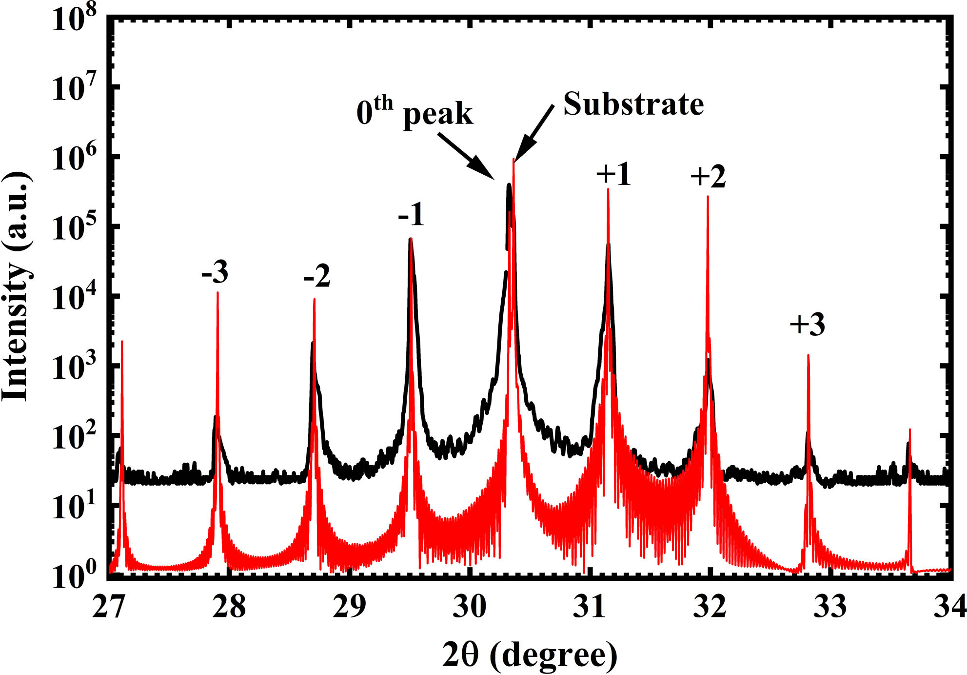
    Fig. 1. HRXRD curve of InAs/InAsSb superlattice grown on GaSb substrate.
    (a) Band diagram of InAs/InAsSb superlattice; (b) schematic of fabricated InAs/InAsSb nBn device; (c) SEM image of passivated mesa sidewall of the device; (d) microscope image of the InAs/InAsSb nBn device.
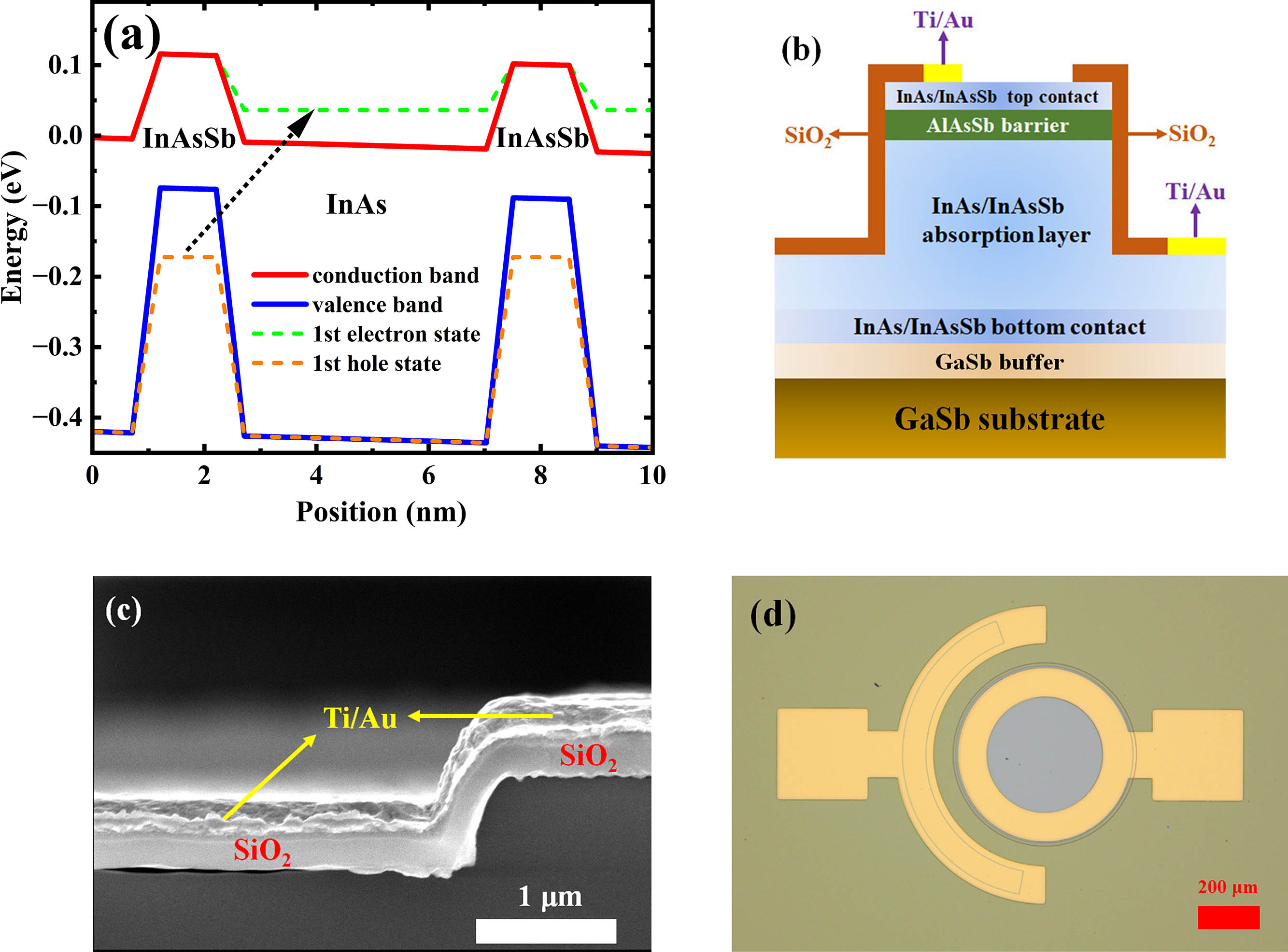
    Fig. 2. (a) Band diagram of InAs/InAsSb superlattice; (b) schematic of fabricated InAs/InAsSb nBn device; (c) SEM image of passivated mesa sidewall of the device; (d) microscope image of the InAs/InAsSb nBn device.
    Temperature dependent (a) dark current and (b) RA characteristic of 200 µm diameter InAs/InAsSb nBn device. The inset of (a) is the dark current density as a function of perimeter-to-area ratio (P/A). (c) Arrhenius plot of 200 µm diameter InAs/InAsSb nBn device under reverse bias of −600 mV.
    Fig. 3. Temperature dependent (a) dark current and (b) RA characteristic of 200 µm diameter InAs/InAsSb nBn device. The inset of (a) is the dark current density as a function of perimeter-to-area ratio (P/A). (c) Arrhenius plot of 200 µm diameter InAs/InAsSb nBn device under reverse bias of −600 mV.
    Photoresponse varying with reverse bias voltage at 237 K.
    Fig. 4. Photoresponse varying with reverse bias voltage at 237 K.
    Detectivity of nBn InAs/InAsSb device at 97 and 237 K.
    Fig. 5. Detectivity of nBn InAs/InAsSb device at 97 and 237 K.
    Ref.Dpixel (µm)Dark Current Density at High Temperature (A/cm2)
    [15]100–4000.44 (−50 mV, 300 K)
    [17]5000.50 (−130 mV, 300 K)
    [24]500.865 (−100 mV, 300 K)
    [25]N/A0.39 (−120 mV, 300 K)
    [26]203.94 (−1 V, 300 K)
    This work2000.31 (−600 mV, 297 K)
    Table 1. Dark Current Characteristics of Different Reported InAs/InAsSb MWIR Photodetectors
    Peng Cao, Tiancai Wang, Hongling Peng, Zhanguo Li, Qiandong Zhuang, Wanhua Zheng. Mid-wavelength nBn photodetector with high operating temperature and low dark current based on InAs/InAsSb superlattice absorber[J]. Chinese Optics Letters, 2024, 22(1): 012502
    Download Citation