
Peng Cao, Tiancai Wang, Hongling Peng, Zhanguo Li, Qiandong Zhuang, Wanhua Zheng. Mid-wavelength nBn photodetector with high operating temperature and low dark current based on InAs/InAsSb superlattice absorber[J]. Chinese Optics Letters, 2024, 22(1): 012502
- Chinese Optics Letters
- Vol. 22, Issue 1, 012502 (2024)
Abstract
Keywords
1. Introduction
Mid-wavelength infrared (MWIR) photodetectors play a crucial role in a wide range of applications, including gas detection, imaging, astronomy, science, and environmental monitoring[1–4]. However, the operating temperature is limited by significantly increasing dark current as the operating temperature rises, which is associated with the nature of the narrow bandgap the materials used. The dark current, typically due to the thermal excitation process, will rise exponentially as the temperature increases.
Over the past decades, many material systems have been exploited to work on MWIR spectra. Bulk narrowband gap InSb-based MWIR photodetectors are currently commercially mature, representing a dark current density of under bias at 77 K[5]. Another commercially matured material option is HgCdTe (MCT). Simulation models were established[6,7] and experimental nBn type MCT devices have subsequently been realized with a saturation dark current about under at 180 K[8]. Moreover, narrow bandgap material InAs is also a candidate for MWIR detection. At room temperature, a dark current density of under and a peak responsivity of 1.47 A/W were obtained from InAs-based devices[9]. A type II superlattice (T2SL) material system based on 6.1 Å (1 Å = 0.1 nm) lattice constant family (i.e. InAs/GaSb/AlSb) has also been utilized on the MWIR spectra. Interband cascade MWIR photodetectors based on InAs/GaSb superlattices have demonstrated a dark current of and under bias at 77 and 295 K, respectively, with a responsivity of 0.167 A/W at 4 µm[10].
However, there are several drawbacks for the material system above that limit the optoelectronic performance of the devices. Less flexibility of tuning the bandgap for a wide spectral response is the main issue for the bulk materials InAs or InSb, while the performance of HgCdTe-based MWIR photodetector devices is restricted by the nonuniform growth of large array and high cost CdZnTe substrate[11]. The T2SL InAs/GaSb system is a good candidate for MWIR detection, but the InAs/GaSb interfaces bring a strong scattering effect that shortens the photon-generated carriers’ lifetime and increases dark current, resulting in a limitation on its operating temperature[12]. Thus, T2SL Ga-free InAs/InAsSb has been investigated since 2012 due to the potential long carrier lifetime of 412 ns[13]. Several attempts on improving the growth quality of InAs/InAsSb have been made to enhance the structural and optical properties of the InAs/InAsSb absorption layer[14]. As for the optoelectronic performance of InAs/InAsSb-based MWIR photodetectors, researchers at Northwestern University have optimized InAs/InAsSb-based MWIR photodetectors with an AlAsSb barrier in both planar and mesa configurations. These detectors demonstrated a dark current density of under at 300 K and at 150 K[15,16]. Jiang et al. demonstrated an InAs/InAsSb-based photodetector with a cutoff wavelength of 3.5 µm, presenting a peak responsivity of 0.56 A/W under a reverse bias voltage of [17]. Huang et al. proposed an MWIR photodetector using an InAs/InAsSb absorption layer and obtained a peak responsivity of 2.16 A/W at a temperature of 160 K[18]. Also, high-speed MWIR photodetectors exploiting higher p-doped InAs/InAsSb absorbers have been reported by Huang et al. that provide a large 3-dB bandwidth[19].
Sign up for Chinese Optics Letters TOC. Get the latest issue of Chinese Optics Letters delivered right to you!Sign up now
In this paper, we reported photodetectors with reduced dark current at higher temperatures using nBn type T2SL InAs/InAsSb MWIR photodetectors. This was achieved through the use of a lattice-matched AlAsSb layer as the electron barrier, which provides a large conduction band offset (CBO) between the InAs/InAsSb absorption layer and the barrier layer, employing an Sb soaking technique to improve the T2SL interfaces, which lowers the Shockley–Read–Hall (SRH)-related recombination current, and using a layer for passivation to suppress the surface leakage current that is related to dangling bonds.
2. Growth and Fabrication
To target MWIR photodetection, we employed a strain-balanced structure of T2SL (n is the thickness of InAsSb, while 3n is the thickness of InAs)[20]. The structure was grown on an n-GaSb substrate by molecular beam epitaxy (MBE). After the deposition of a 200 nm n-GaSb buffer layer, a 200 nm thick heavily n-doped InAs/InAsSb bottom contact layer was deposited, followed by a 1 µm thick unintentionally doped InAs/InAsSb T2SL layer. Then an undoped 10 nm-AlAsSb lattice matched to GaSb was grown, followed by a top contact layer of heavily n-doped InAs/InAsSb T2SL with narrower period thickness, which has wider bandgap energy acting as a window layer as well. The growth condition was set at a pre-optimized temperature of 400°C–430°C with a growth rate of 1 µm/h and a beam equivalent pressure (BEP) of for Sb. An Sb soaking technique that we developed previously was applied to improve the interfaces of the T2SL[21]. After the growth of InAs, both In and As shutters closed for 20 s to purge residual As; then 3 s later, Sb was deposited and followed by immediate growth of InAsSb. The mesa was dry-etched by an inductive coupled plasma (ICP) instrument, and then a 400 nm thick passivation layer was deposited over the sidewall by plasma-enhanced chemical vapor deposition (PECVD).
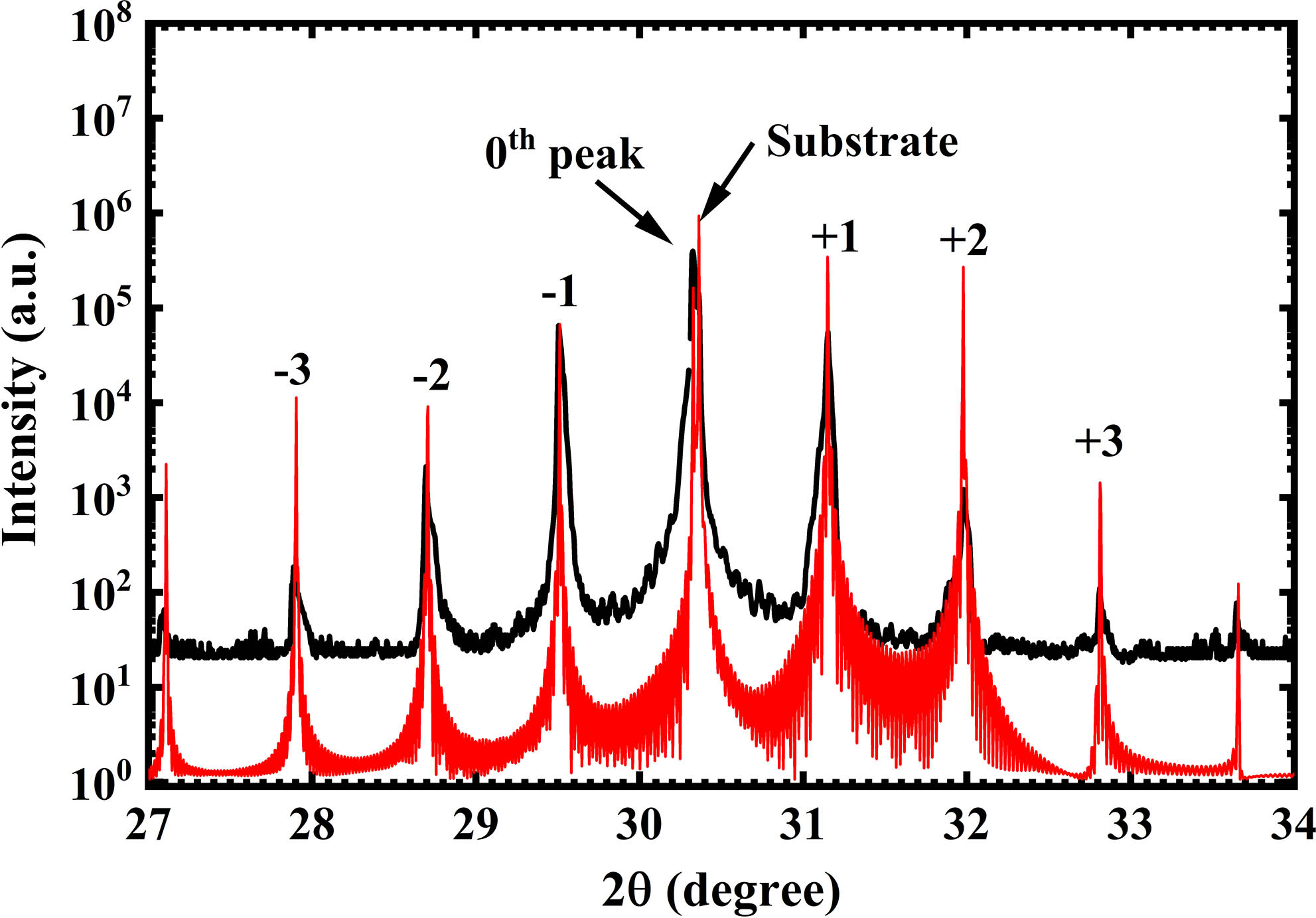
Figure 1 shows the high-resolution X-ray diffraction (HRXRD) pattern, which indicates the crystalline quality of the epilayer materials. The narrow superlattice 0th peak with a full width at half-maximum (FWHM) of 62 arcsec indicates an extremely high crystalline quality of InAs/InAsSb superlattice and abrupt interfaces.
![]()
Figure 1.HRXRD curve of InAs/InAsSb superlattice grown on GaSb substrate.
Furthermore, the small angular separation between the superlattice 0th peak and the GaSb substrate reflects the well strain-balanced InAs/InAsSb superlattice with respect to the GaSb substrate. As shown in Fig. 1, this angular separation value is found to be about 126 arcsec, which leads to a lattice mismatch of 0.10% according to Eq. (1)[22]. This indicates the InAs/InAsSb absorption layer is closely lattice matched to GaSb,
The simulation result reveals the T2SL has a structure of .
Figure 2(a) shows the simulation results of the T2SL band diagram using SILVACO TCAD 2022 software. It reveals a cutoff wavelength at about 5.9 µm at 300 K, which covers the important atmospheric window of 3–5 µm and a spectral range that gives strong absorption to most molecules.
![]()
Figure 2.(a) Band diagram of InAs/InAsSb superlattice; (b) schematic of fabricated InAs/InAsSb nBn device; (c) SEM image of passivated mesa sidewall of the device; (d) microscope image of the InAs/InAsSb nBn device.
The schematic configuration of the fabricated mesa type nBn InAs/InAsSb device is shown in Fig. 2(b). The scanning electron microscope (SEM) image of the passivated mesa sidewall and the microscope image of the device are shown in Figs. 2(c) and 2(d), respectively.
3. Device Characteristic and Discussion
Temperature-dependent dark current characteristics and the differential resistance area product (RA) of a 200 µm diameter InAs/InAsSb nBn device are shown in Figs. 3(a) and 3(b). At 97 K, the device shows a dark current density of and an RA of under a bias of . At 297 K, under , the dark current density increased to and a reduced RA of was obtained under similar bias. The inset of Fig. 3(a) represents the dark current density under as a function of perimeter to area ratio (P/A) according to Ref. [23]. The dark current density shows an ultraweak dependence on the detector size, leading to an ultralow extracted surface current density. This is associated with the precisely controlled ICP etching process and the high quality of the densely deposited passivation layer over the mesa sidewall. Figure 3(c) shows the Arrhenius plot of the photodetector under a reverse bias of . The extracted activation energy Ea of 239 meV can be concluded in the temperature range of 157 to 297 K. This is close to the energy bandgap of the designed InAs/InAsSb superlattice structure, which reveals that diffusion current dominates the whole dark current in the temperature range. At lower operating temperatures, e.g. from 157 to 97 K, Ea reduces to 53 meV, indicating a tunneling dark current component dominates in this temperature range. This suggests that the generation-recombination (G-R) current is eliminated due to the nBn structure.
![]()
Figure 3.Temperature dependent (a) dark current and (b) RA characteristic of 200 µm diameter InAs/InAsSb nBn device. The inset of (a) is the dark current density as a function of perimeter-to-area ratio (P/A). (c) Arrhenius plot of 200 µm diameter InAs/InAsSb nBn device under reverse bias of −600 mV.
Table 1 summarizes the dark current characteristics of InAs/InAsSb MWIR devices from several research works; our InAs/InAsSb nBn MWIR photodetectors demonstrate an ultralow dark current density compared to that of other groups.
| Ref. | Dpixel (µm) | Dark Current Density at High Temperature (A/cm2) |
|---|---|---|
| [ | 100–400 | 0.44 (−50 mV, 300 K) |
| [ | 500 | 0.50 (−130 mV, 300 K) |
| [ | 50 | 0.865 (−100 mV, 300 K) |
| [ | N/A | 0.39 (−120 mV, 300 K) |
| [ | 20 | 3.94 (−1 V, 300 K) |
| This work | 200 | 0.31 (−600 mV, 297 K) |
Table 1. Dark Current Characteristics of Different Reported InAs/InAsSb MWIR Photodetectors
Figure 4 shows the spectral photoresponse under different reverse biases at 237 K. A cutoff wavelength of 5.5 µm that is consistent with the bandgap simulation was obtained for this nBn InAs/InAsSb device. With the increasing reverse bias, the photoresponse increases simultaneously and nearly saturates at a reverse bias voltage of around . A peak responsivity of 0.39 A/W was obtained at 237 K.
![]()
Figure 4.Photoresponse varying with reverse bias voltage at 237 K.
Figure 5 shows the calculated detectivity of this nBn InAs/InAsSb photodetector device under reverse bias voltage of at an operating temperature of 97 and 237 K, respectively. At 97 K, the peak detectivity is about , while peak detectivity decreases to as the temperature rises up to 237 K.
![]()
Figure 5.Detectivity of nBn InAs/InAsSb device at 97 and 237 K.
4. Conclusion
In summary, we demonstrated nBn T2SL InAs/InAsSb MWIR photodetectors containing an AlAsSb electron barrier with several attempts to suppress dark current density and increase operating temperature. An ultralow dark current density of and was obtained under reverse bias at 97 and 297 K, respectively. This dark current density level is lower than that of the reported InAs/InAsSb MWIR photodetectors, to the best of our knowledge. The device under study showed a cutoff wavelength of 5.5 µm. Also, peak responsivity of 0.39 A/W and peak detectivity of were obtained of this nBn InAs/InAsSb device at a high operating temperature of up to 237 K.
References
[22] P. Christol, F. de Anda, V. Compean et al. Antimonide-based superlattice infrared barrier photodetectors. Proceedings of the 8th International Conference on Photonics, Optics and Laser Technology, 45(2020).

Set citation alerts for the article
Please enter your email address
© Copyright 2018-2021 | Chinese Laser Press. All Rights Reserved 沪ICP备15018463号-20