
Fengyou Yang, Haoran Zhang, Huimin Feng, Jianjie Dong, Chuang Wang, Qian Liu, "Bionic SERS chip with super-hydrophobic and plasmonic micro/nano dual structure," Photonics Res. 6, 77 (2018)
- Photonics Research
- Vol. 6, Issue 2, 77 (2018)
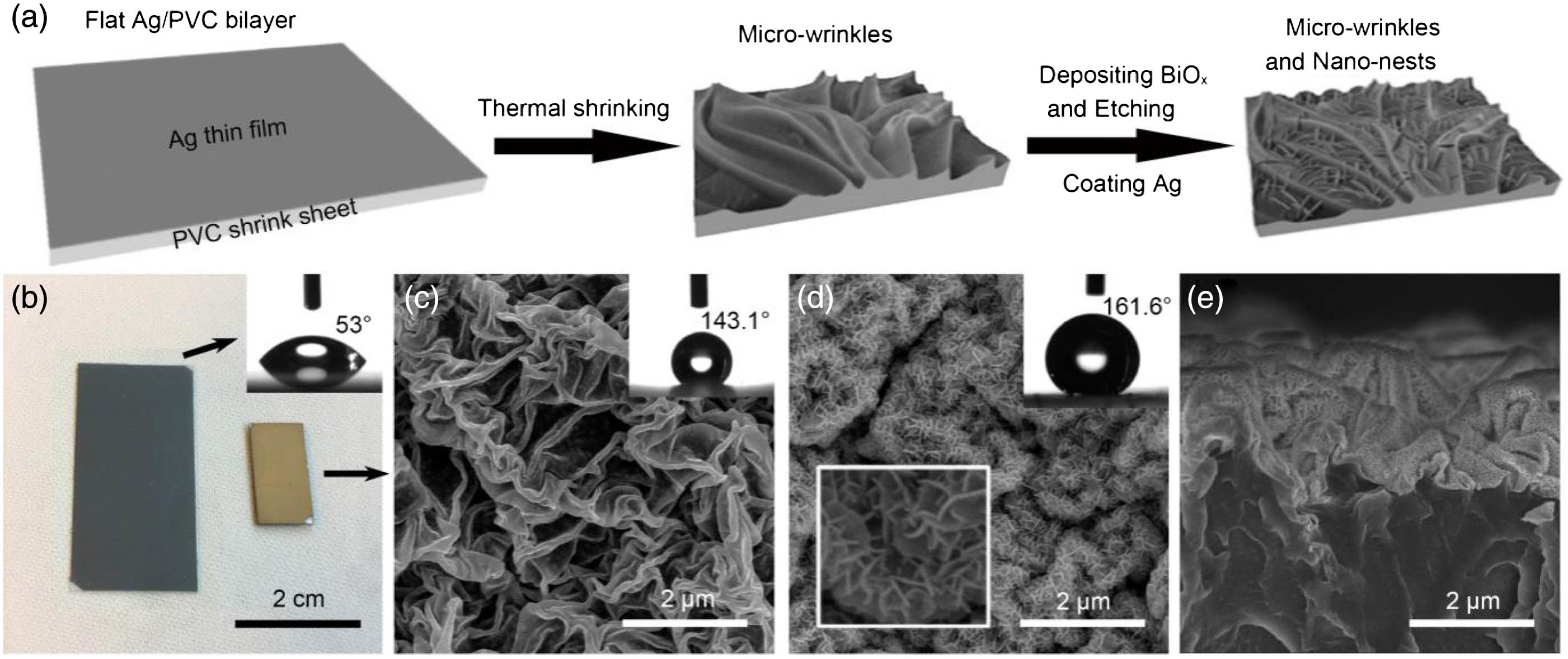
Fig. 1. (a) Fabrication procedure of the bionic SERS chip with micro-wrinkles and nano-nests dual structure. (b) Optical photograph of Ag/PVC bilayers before (left) and after (right) thermal shrinking. Inset: CA of the flat sample. (c) SEM image of the micro-wrinkled structure. Inset: CA of the sample with micro-wrinkles. (d) SEM image of the dual structure with micro-wrinkles and nano-nests. Inset (top right): CA of the sample with dual structure. Inset (down left): magnified SEM image of nano-nests. (e) Cross-sectional SEM image of the bionic SERS chip with dual structure.
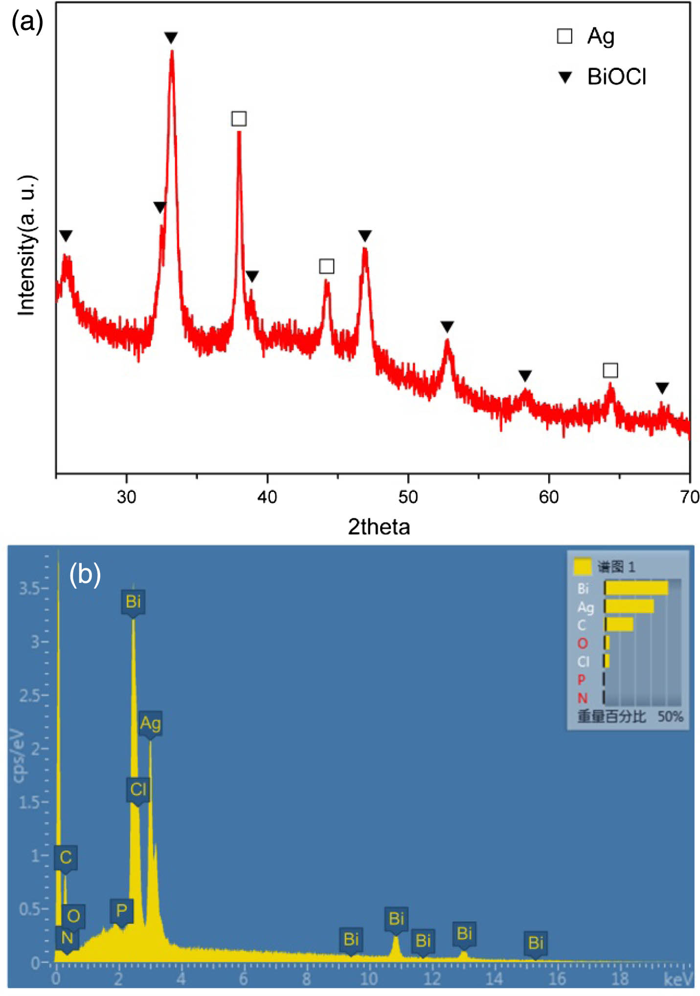
Fig. 2. Component analyses via (a) XRD and (b) EDS of the bionic SERS chip.
Fig. 3. (a)–(e) SEM images and corresponding CAs of Ag/PVC micro-wrinkle structures with Ag thickness of 10, 20, 30, 40, and 50 nm, respectively. (f)–(j) SEM images and corresponding CAs of the bionic dual-structure chips with micro-wrinkles and nano-nests. (k) The experimental and theoretical results of wrinkle period for the five Ag/PVC samples with different Ag film thickness in (a)–(e). (l) CA curves of the samples only with micro-wrinkle [black, (a)–(e)] and with dual structure [red, (f)–(j)], respectively. (m) Raman signal intensity of 10 − 6 M
Fig. 4. (a) SERS spectra for different R6G concentrations (10 − 6 10 − 7 10 − 8 10 − 9 M 10 − 8 M 10 − 9 M
Fig. 5. (a) SEM image of chip surface with micro-wrinkle and nano-nest. (b) SEM image of chip surface with only the micro-wrinkle. (c) SEM image of chip surface with only nano-nest. (d) R6G Raman spectra for the chip with micro/nano dual structure, only micro-wrinkle and only nano-nest, respectively.
Fig. 6. (a) SEM image of the silver nano-nest structure on the bionic chip. (b) Simulation structure of the nano-nest consisting of several Y-shaped nanostructures for FDTD. (c)–(f) The normalized electric field | E | / | E 0 |


Set citation alerts for the article
Please enter your email address

© Copyright 2018-2021 | Chinese Laser Press. All Rights Reserved 沪ICP备15018463号-20