• Chinese Optics Letters
  • Vol. 19, Issue 11, 114001 (2021)
Zhaojing Hu, Yunxiang Zhang, Shuping Lin, Shiqing Cheng, Zhichao He, Chaojie Wang, Zhiqiang Zhou, Fangfang Liu, Yun Sun, and Wei Liu*
Author Affiliations
  • Institute of Photoelectronic Thin Film Devices and Technology of Nankai University, Key Laboratory of Photoelectronic Thin Film Devices and Technology of Tianjin, Engineering Research Center of Thin Film Photoelectronic Technology, Ministry of Education, Tianjin 300350, China
  • show less
    DOI: 10.3788/COL202119.114001 Cite this Article Set citation alerts
    Zhaojing Hu, Yunxiang Zhang, Shuping Lin, Shiqing Cheng, Zhichao He, Chaojie Wang, Zhiqiang Zhou, Fangfang Liu, Yun Sun, Wei Liu. Incorporation of Ag into Cu(In,Ga)Se2 films in low-temperature process[J]. Chinese Optics Letters, 2021, 19(11): 114001 Copy Citation Text show less

    Abstract

    Chalcopyrite Cu(In,Ga)Se2 (CIGS) thin films deposited in a low-temperature process (450°C) usually produce fine grains and poor crystallinity. Herein, different Ag treatment processes, which can decrease the melting temperature and enlarge band gap of the CIGS films, were employed to enhance the quality of thin films in a low-temperature deposition process. It is demonstrated that both the Ag precursor and Ag surface treatment process can heighten the crystallinity of CIGS films and the device efficiency. The former is more obvious than the latter. Furthermore, the Urbach energy is also reduced with Ag doping. This work aims to provide a feasible Ag-doping process for the high-quality CIGS films in a low-temperature process.

    1. Introduction

    Nowadays, the fascinating thin films for photovoltaic generation are Cu(In,Ga)Se2 (CIGS) thin film[1,2], perovskite thin film[3,4], GaAs thin film[5], and so on. Compared with other films, polycrystalline CIGS thin film is more attractive because of its high-power conversion efficiency[1,2], high stability of heat and damp[6,7], and low cost of manufacturing process[8,9]. Typical efficient CIGS thin films are usually prepared at a substrate temperature of over 550°C[2,10], but the deformation of the soda-lime glass (SLG) substrate and high cost of the manufacturing process can restrict the process of industrial production of CIGS thin film solar cells[11]. A low-temperature deposition process, which is growing CIGS films at temperatures below 450°C, provides feasibility for the reduction of energy consumption and the application of flexible CIGS solar cells on a non-heat-resistance substrate, such as polyimide foil (PI)[9,12].

    However, a low-temperature deposition process often produces an inferior device performance due to the poor crystallinity of CIGS films with the absence of the Cu2xSe liquid phases during the deposition process[1315]. When the substrate temperature is below 523°C, the excess Cu2xSe phases during the second stage will be transformed to the solid phases[16], which cannot assist the CIGS grain growth and yield fine grains[17]. The fine grains of CIGS film contain a large amount of grain boundaries, increasing the recombination losses and resulting in lower conversion efficiency[11,18]. Recently, the incorporation of silver (Ag) into CIGS films has become the hot topic to address the poor crystallinity issue because the incorporation of silver into CIGS films to form (Ag,Cu)(In,Ga)Se2 (ACIGS) can lower the melting temperature and enlarge the band gap of absorber layers[19,20]. Usually, there are many methods used to deposit the Ag-based compounds on the substrate, such as the evaporation process[18], sputtering process[1], spin-coating process[21], ligand mediated colloidal sol-gel method[22], and laser ablation[23,24]. According to the deposition process of the absorber layer, the appropriate method can be selected to add the Ag element into the CIGS films. Many researches have improved the device performance of CIGS solar cell by Ag doping with suitable deposition methods. Zhao et al. achieved high-efficiency CIGS solar cells through Ag passivating the bulk defect by the spin-coating process[21]. Both Kihwan Kim and Gayeon Kim deposited the thin Ag precursor layer to assist the growth of CIGS thin film in a low-temperature co-evaporation process and improved the device efficiency[18,25]. In addition, our previous work used Ag surface-treated CIGS thin films to passivate bulk defects of the CIGS/CdS heterojunction interface and realized a device efficiency of 17.4%[26]. To further improve the device performance of low-temperature deposited CIGS solar cells, it is very useful to research the diffusion mechanism of Ag in CIGS thin films at this process.

    In this work, we investigate the effects of different Ag treatment processes (the Ag precursor and the Ag surface treatment process) on the material and the corresponding device properties during low-temperature processes. First, the material properties of different Ag treatment processes are investigated. Subsequently, the correlation with device performance, such as short-circuit current density (JSC) and open-circuit voltage (VOC), is also addressed systematically. Finally, combining the analysis of the material properties and the device measurement data, the comprehension of the growth mechanism of different Ag treatment processes is obtained. Herein, we aim at providing a simple and effective way to deposit high-quality CIGS film at low temperature.

    2. Experimental Methods

    2.1. Preparation of CIGS films and solar cells

    In this study, the solar cell has a Ni-Al/Al-ZnO/i-ZnO/CdS/CIGS/Mo/SLG structure with the active area of 0.34cm2[2729]. First, the molybdenum (Mo) layer (about 800 nm) was grown onto the SLG substrate with a direct current (DC) sputtering. Afterwards, we brought the Mo-coated SLG substrate into a vacuum chamber to deposit absorber layers in a low-temperature deposition process (450°C). As depicted in Fig. 1, to form the Ag–Se precursor films, Ag was evaporated at a evaporator temperature of 1000°C with a high Se ambient condition of 3.5×10³Pa. The growth rate of the Ag–Se precursor films was 25nm·min1. Then, three-stage deposition process was applied to growing high-quality CIGS films. In the first stage, the precursor layer (In0.7,Ga0.3)2Se3 with a thickness of 1.2 µm was deposited by co-evaporating In, Ga, and Se elements at the substrate temperature of 450°C for 20 min. In the second stage, keeping the substrate temperature constant, the CIGS film was formed by evaporating Cu and Se on the precursor layer. The second stage was ended until the film had a transition to a Cu-rich composition, and it took 25 min. In the third stage, In, Ga, and Se elements were again evaporated for 15 min to make the CIGS film convert from Cu-poor to Cu-rich and obtain CIGS film with a stoichiometric ratio. In addition, the Ag surface treatment process was carried on the surface of CIGS films, which was the same as the deposition process of the precursor films. More details about the deposition of absorber layers can be observed in Fig. 1. After the CIGS deposition process, a 50 nm n-type CdS was prepared by a chemical bath deposition (CBD) process. Subsequently, the ZnO (50 nm) and Al-doped ZnO (400 nm) were grown by a radio frequency (RF) sputtering method. Lastly, the Ni–Al grids were evaporated with a mask by the electron beam evaporation process.

    Sketch diagram of the absorber layer deposition process. The PRE-Ag process is referring to the Ag–Se precursor deposition process, which was prepared before the CIGS deposition process. In addition, the Ag surface treatment process carried out on the surface of CIGS films is denoted as the PDT-Ag process.

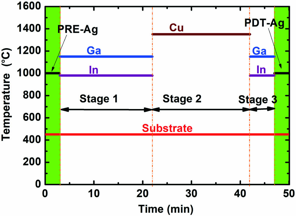
    Figure 1.Sketch diagram of the absorber layer deposition process. The PRE-Ag process is referring to the Ag–Se precursor deposition process, which was prepared before the CIGS deposition process. In addition, the Ag surface treatment process carried out on the surface of CIGS films is denoted as the PDT-Ag process.

    In this work, three group samples were prepared to study the characteristics of Ag-doped CIGS films in a low-temperature deposition process. The detailed deposition conditions of different samples are supplied in Table 1. Here, the CIGS sample without any treatment was used as the reference sample. Then, the influence of Ag on CIGS material properties was compared by the samples, A, B, and C. For all samples, the molar ratio of Ga and In + Ga (GGI) is in the range of 0.32–0.33. In addition, the thickness of all films ranges from 2.0 to 2.2 µm.

    SamplePRE-Ag (50 nm)PDT-Ag (50 nm)
    ANoNo
    BYesNo
    CNoYes

    Table 1. Deposition Conditions of Different Samples with Aga

    Ag-Treated SampleΔEU (meV)ΔVOC (mV)
    B13.512
    C14.712

    Table 2. Statistics of Different CIGS Samples in the ΔEU and ΔVOCa

    2.2. Characterization

    The integral compositions of CIGS films with Ag were determined by X-ray fluorescence spectroscopy (XRF), which was calibrated by inductively coupled plasma (ICP). A scanning electron microscope (SEM) was used to show the cross sections of Ag-treated films. The crystallinities of absorber layers were characterized by a Philips X-pert pro X-ray diffractometer (XRD) with a CuKα. A 2420 source meter under air mass (AM) 1.5 illumination (100mW·cm2) was employed to determine the current-voltage (J-V) curves of solar cells. An HP 4284A inductance, capacitance, resistance (LCR) meter was applied on ACIGS films to determine defect concentrations and its distributions (capacitance-voltage, CV; admittance spectroscopy characterizations, AS). Furthermore, the external quantum efficiency (EQE) of different samples was measured in the range of 350–1300 nm.

    3. Result and Discussion

    3.1. Independently controlling material properties of CIGS films with Ag

    Figure 2(a) shows the XRD patterns of CIGS films to explore the phase transition of Ag-treated CIGS films. Except for the Mo peak (about 40°), all XRD patterns of the three samples (A, B, and C) are consistent with chalcopyrite CIGS phases[21], which means that Ag was well synthesized into the CIGS films. The reference CIGS sample (A) exhibits an obvious (220/204) preferred orientation, while Ag-treated samples (B and C) have a strong (112) preferred orientation. In fact, the (112) peak in chalcopyrite film has the lowest surface energy[18]. When Ag is incorporated into CIGS film, the melting temperature of the absorber layer is reduced obviously, leading to the enhanced element diffusion. As a result, the film has a lower surface energy. Therefore, ACIGS films show different preferred orientation (112) in contrast with the reference CIGS sample. The corresponding grazing incident X-ray diffraction (GIXRD) patterns of CIGS films with the incident angle of 0.3° are presented in Fig. 2(b). The significant shift to a lower degree in ACIGS films indicates the successful substitution of Ag for Cu. In addition, the peak of sample C [post deposition treatment (PDT)-Ag process] is slightly lower than that of the sample B [precursor deposition treatment (PRE)-Ag process], which suggests that the Ag content of the sample C is a little higher on the CIGS surface. It is known that the diffusion of the Ag element in CIGS films deposited at the high substrate temperature is uniform, which is not affected by the different Ag treatment processes. Therefore, the Ag content on the surface of CIGS thin films with different Ag treatment processes should be equivalent at the high substrate temperature. In this low-temperature deposition process, the Ag content of sample C (PDT-Ag process) is a little higher on the CIGS surface than that of sample B (PRE-Ag process), although they possesses almost the same Ag content as sample C. Therefore, it is likely that the low substrate temperature limits the diffusion of the Ag element in CIGS films. According to the standard equation of the tetragonal lattice (1d2=h2+k2a2+l2c2)[26], the lattice constants of CIGS films can be calculated: sample A, 5.7120 (1 Å = 10−10 m) for a and 11.3315 for c; sample B, 5.7398 for a and 11.4235 for c; and sample C, 5.7319 for a and 11.5409 for c. These results indicate that substituting Ag for Cu can increase the lattice constants of CIGS films. Besides, the corresponding values of c/2a of different samples (A, B, and C) are 0.9919, 0.9951, and 1.0006, respectively. Considering that the CIGS film is chalcopyrite structure, the ideal lattice constant c/2a is one[30]. It is found that the incorporation of Ag into CIGS film could address lattice distortions, which also verifies our previous work[26].

    (a) XRD patterns of the CIGS films with Ag. (b) The corresponding grazing incident X-ray diffraction (GIXRD) patterns of absorber layers.

    Figure 2.(a) XRD patterns of the CIGS films with Ag. (b) The corresponding grazing incident X-ray diffraction (GIXRD) patterns of absorber layers.

    Cross-sectional SEM images of CIGS films are given in Fig. 3. Clearly, the crystallinity of the reference CIGS film, grown in a low-temperature process, is poor in Fig. 3(a). The grain sizes in the upper part of the film are larger than that near the Mo layer owing to the Ga distribution in the absorber layer. For the Ag precursor-treated sample B, its crystallinity is improved obviously, and the fine grain layer near the Mo layer disappears. In addition, the grains in the upper part of sample B also become better. Currently, two possible explanations can be considered for this phenomenon. First, the melting temperature of the whole films is decreased after the incorporation of Ag, which can enhance the recrystallization. In addition, it has been demonstrated that the Cu–Se phases are also observed in the Cu-poor condition during the second stage[31]. Given the fact that the bond dissociation energy of the Ag–Se phases is lower than that of the Cu–Se phases[25,32,33], we can deduce that more Ag atoms of sample C with the PDT-Ag process can be separated to the lattice of Cu to improve the quality of CIGS films. Compared with the reference CIGS sample A, sample C possesses similar crystal quality (the poor microstructure near the Mo layer). The increased grain size in the upper part of sample C means that the Ag surface process in a low-temperature process mainly improves the upper CIGS crystallization, which agrees with the XRD results in Fig. 2(b). In combination with the result of sample C, it is obvious that both the Ag precursor and the Ag surface process can heighten the crystallinity of CIGS film, and the former is more obvious than the latter. Therefore, incorporating Ag into CIGS films can contribute to improving the crystallization of the absorber layers.

    Cross-sectional SEM images of CIGS films of (a) A, (b) B, and (c) C.

    Figure 3.Cross-sectional SEM images of CIGS films of (a) A, (b) B, and (c) C.

    3.2. Device performance of Ag-treated CIGS solar cells

    The photovoltaic parameters of Ag-treated CIGS films are shown in Fig. 4. It can be observed that the conversion efficiency of Ag-treated CIGS samples increases from 14.0% to 15.1%, mostly because of the enhanced short-circuit current density (JSC). In order to give an explanation for the changed JSC, EQE results are exhibited in Fig. 5(a). Compared with the reference CIGS sample, the Ag-treated samples have a blue shift of the band-edge wavelength, leading to the reduction of JSC. This is related to the enlarged band gap caused by Ag doping. The band gap values of different samples were obtained by EQE curve fitting. As shown in Fig. 5(b), after adding Ag into CIGS films, values of the band gap increase slightly. Besides, the improved spectral response of the near-infrared wavelengths (600–900 nm) of Ag-treated CIGS films indicates that Ag can improve the minority carrier collection of the bulk of CIGS films due to the enhanced recrystallization[18]. Therefore, the improved JSC mainly benefits from the increased minority carrier collection.

    (a) J-V curves of the best CIGS solar cells fabricated from the different absorber samples. Statistic boxes for the (b) VOC, (c) JSC, and (d) FF and each box contains over 10 solar cells.

    Figure 4.(a) J-V curves of the best CIGS solar cells fabricated from the different absorber samples. Statistic boxes for the (b) VOC, (c) JSC, and (d) FF and each box contains over 10 solar cells.

    (a) External quantum efficiency (EQE) spectrum. (b) The band gap value obtained by EQE fitting curve. (c) Doping concentration (Na) of different samples. (d) ln(EQE) as a function of photon energy to determine the Urbach energy (EU) values.

    Figure 5.(a) External quantum efficiency (EQE) spectrum. (b) The band gap value obtained by EQE fitting curve. (c) Doping concentration (Na) of different samples. (d) ln(EQE) as a function of photon energy to determine the Urbach energy (EU) values.

    In addition, adding Ag into CIGS films also increases the VOC slightly, as shown in Figure 4(b). This result can be attributed to the enlarged band gap, the reduced defect concentration, and the enhanced CdS/CIGS heterojunction, which have been discussed in detail in our previous work[27,34]. It is well known that the Urbach energy (EU) of CIGS films, which is calculated by the EQE results in the long-wavelength edge, can be used to measure the change in VOC,def (VOC,def=Eg/qVOC). Here, a decreased VOC,def corresponds to an improved VOC. In order to further explore the reason for the changed VOC, the EU of different samples should be calculated by the following equation: ln(EQE)=c+hvEU,where hv and c are photon energy and constant, respectively. The corresponding EU results are shown in Fig. 5(d). Clearly, with the Ag precursor layers, the EU values of CIGS thin films are decreased from 36.2 to 22.7 meV, mainly due to the enlargement of grain sizes, as shown in Figs. 3(a) and 3(b). It is evident that the Ag surface treatment process also induces the reduction of the EU value (21.5 meV), which does not seem to be related to the crystallinity of CIGS films in Figs. 3(a) and 3(c). According to the result of Kim et al. and our previous work, Ag surface treatment can passivate the defect at the CIGS/CdS heterojunction effectively[18,23]. This result manifests that the EU of solar cells also can be used to reflect the quality of the CIGS/CdS heterojunction.

    From previous work[35], the decrease in the EU value of the CIGS films by 1 meV corresponds to the reduction of VOC,def by 8.6 mV. This result indicates that when the EU value reduces 1 meV, the VOC of solar cells should increase about 8.6 mV. As shown in Table 2, to get clearer comparison, we calculated the ΔEU (the reduced Urbach energy) and ΔVOC (the increased VOC) of different samples. The ΔEU for samples B and C is 13.5 and 14.7 meV, respectively, while their ΔVOC are both 12 mV. It suggests that the reduced EU does not contribute sufficiently to the increased VOC.

    Exploring the reason for the slightly improved VOC, CV results of different samples are provided in Fig. 5(c). The doping concentrations (Na) are 2.14×10¹⁵, 4.02×10¹⁴, and 1.32×1015cm3 for samples A, B, and C, respectively. From the previous studies[30,36,37], the relationship between the VOC and Na can be expressed as follows: ΔVOC=VOC2VOC1=kTqln(Na2Na1),where k, T, and q are the Boltzmann constant, temperature, and elementary charge, respectively. A higher Na brings a higher VOC[30]. However, when Ag was incorporated into CIGS thin film, the carrier concentration decreased significantly. We attribute the slightly improved VOC to the low p-type conductivity of the absorber layers. It can be observed that the series resistance (RS) of different samples is sample A > sample C > sample B at the same test temperature (from 120 K to 300 K). This difference determines the fill factor of solar cells. The larger RS of solar cells is often determined by the contact and bulk resistances of the stack layers, and it obviously affects the transport of the carrier. Furthermore, the charge barrier height Φb of each sample is also calculated in Fig. 6. It shows that the values of barrier height of samples A, B, and C are 80, 74, and 78 meV, respectively. The hole concentrations of all samples from CV results are found to be 2.14×10¹⁵, 4.02×10¹⁴, and 1.32×1015cm3, respectively. These results are in accordance with the investigation of Zhang et al., where the back-contact barrier may be attributed to the carrier density[38]. For reference sample A, the crystallinity is poor, and many fine grains are carried throughout the film in Fig. 3(a). The grain boundary recombination is serious. When it comes to sample C, the Ag surface treatment improves the surface quality of CIGS films in Fig. 3(c) and promotes the carrier transport at the front surface. However, the crystallinity of sample C near the Mo layer is still poor. Thus, the decreased barrier height is not obvious. When Ag was introduced before the CIGS process (sample B), the enhanced crystallinity further induces the barrier height from 78 meV to 74 meV. This phenomenon indicates that the incorporation of Ag enhances CIGS films’ crystallinity, which is the reason for the varied carrier concentration and the changed carrier transport from the active layer to the back electrode in Figs. 5(c) and 6. Therefore, the enlarged VOC of Ag-treated CIGS solar cell is largely thanks to the improvement of the qualities of CIGS films and the CIGS/CdS heterojunction. However, the low carrier concentration of the absorber layers limits the increase of VOC. To enhance the p-type conductivity of the CIGS films, PDT for Na should be a simple method, which deserves further investigation.

    Charge barrier height Φb of different samples.

    Figure 6.Charge barrier height Φb of different samples.

    4. Conclusion

    In this paper, different Ag treatment processes were utilized to improve the CIGS material properties and the corresponding device performance in a low-temperature process. The incorporation of Ag into CIGS films can not only reduce the melting temperature of the absorber layer but also enhance the element diffusion. Simultaneously, it leads to a lower surface energy and generates a strong (112) preferred orientation. Furthermore, according to the XRD results, we can observe the larger lattice constant of the CIGS films compared with the reference sample, which suggests that the addition of Ag can increase the lattice constant of CIGS films. In contrast to the reference film, the values of c/2a of Ag-doping CIGS films are closer to one (the ideal lattice constant of CIGS film). It is demonstrated that both the Ag precursor and the Ag surface process can heighten the crystallinity of CIGS film, and the former is more obvious than the latter. The enhanced crystallinity of CIGS films is beneficial to the collection of minority carriers and the improvement of JSC. Furthermore, EU is also reduced with Ag doping: the Ag precursor process decreases the EU value from 36.2 to 22.7 meV because of the enhanced crystallinity, and, for sample C, the EU value decreases from 36.2 to 21.5 meV, which attributes to the passivation of the defect at the CIGS/CdS heterojunction. However, the reduced EU does not make sufficient contributions to the increased VOC for the CIGS thin films with Ag doping, which is ascribed to the decreased carrier concentration. Besides, compared with the reference CIGS films, the values of charge barrier height Φb from the absorber layers to Mo back electrodes of Ag-treated CIGS films decrease slightly, which may be attributed to the carrier density and affect the transport of the carrier. Therefore, additional Na, not in the SLG substrate, can be introduced into CIGS thin films to improve the carrier concentration. Herein, we expect to provide a simple and effective Ag treatment process for the CIGS film in a low-temperature process.

    References

    [1] M. Nakamura, K. Yamaguchi, Y. Kimoto, Y. Yasaki, T. Kato, H. Sugimoto. Cd-free Cu(In,Ga)(Se,S)2 thin-film solar cell with record efficiency of 23.35%. IEEE J. Photovoltaics, 9, 1863(2019).

    [2] Y. Wang, S. Lv, Z. Li. Review on incorporation of alkali elements and their effects in Cu(In,Ga)Se2 solar cells. J. Mater. Sci. Technol., 96, 179(2021).

    [3] H. Fan, Y. Mu, C. Liu, Y. Zhu, G. Liu, S. Wang, Y. Li, P. Du. Random lasing of CsPbBr3 perovskite thin films pumped by modulated electron beam. Chin. Opt. Lett., 18, 011403(2020).

    [4] P. Liang, C. Chueh, T. S. Williams, K.-Y. Alex. Roles of fullerene-based interlayers in enhancing the performance of organometal perovskite thin-film solar cells. Adv. Energy Mater., 5, 1402321(2015).

    [5] Z. Zhang, Z. Lü, X. Yang, H. Chai, L. Meng, T. Yang. 25 Gb/s directly modulated ground-state operation of 1.3 µm InAs/GaAs quantum dot lasers up to 75°C. Chin. Opt. Lett., 18, 071401(2020).

    [6] B. S. Tosun, R. Feist, A. Gunawan, K. Mkhoyan, S. A. Campbell, E. Aydil. Improving the damp-heat stability of copper indium gallium diselenide solar cells with a semicrystalline tin dioxide overlayer. Sol. Energy Mater. Sol. Cells, 101, 270(2012).

    [7] M. Schmidt, D. Braunger, R. Schäffler, H. W. Schock, U. Rau. Influence of damp heat on the electrical properties of Cu(In,Ga)Se2 solar cells. Thin Solid Films, 361–362, 283(2000).

    [8] H. Y. Sun, P. H. Li, Y. M. Xue, Z. X. Qiao, S. Liu. Effect of MoSe2 on the performance of CIGS solar cells. Optoelectron. Lett., 15, 428(2019).

    [9] Y. Zhang, S. Lin, Z. Hu, S. Cheng, Z. He, Z. Zhou, W. Liu, Y. Sun. Towards an optimized gallium gradient for Cu(In,Ga)Se2 thin film via an improved constant low-temperature deposition process. Sol. Energy Mater. Sol. Cells, 209, 110425(2020).

    [10] P. Jackson, D. Hariskos, R. Wuerz, O. Kiowski, A. Bauer, T. M. Friedlmeier, M. Powalla. Properties of Cu(In,Ga)Se2 solar cells with new record efficiencies up to 21.7%. Rapid Res. Lett., 9, 28(2015).

    [11] L. Zhang, Q. He, W. L. Jiang, F. F. Liu, C. J. Li, Y. Sun. Effects of substrate temperature on the structural and electrical properties of Cu(In,Ga)Se2 thin films. Sol. Energy Mater. Sol. Cells, 93, 114(2009).

    [12] W. Li, L. Yao, K. Li, X. Li, B. Yang, S. Xu, S. Shi, C. Yi, M. Chen, Y. Feng, W. Li, Z. Lu, C. Yang. Enabling low-temperature deposition of high-efficiency CIGS solar cells with a modified three-stage co-evaporation process. ACS Appl. Energy Mater., 3, 4201(2020).

    [13] A. Chirila, D. Guettler, D. Brémaud, S. Buecheler, R. Verma, S. Seyrling, S. Nishiwaki, S. Haenni, G. Bilger, A. N. Tiwari. CIGS solar cells grown by a three-stage process with different evaporation rates. 2009 34th IEEE Photovoltaic Specialists Conference (PVSC), 11152452(2009).

    [14] V. Achard, M. Balestrieri, S. Béchu, M. Jubault, M. Bouttemy, L. Lombez, T. Hildebrandt, N. Naghavi, A. Etcheberry, D. Lincot, F. Donsanti. Effect of Ga introduction during the second stage of a coevaporation process of Cu(In,Ga)Se2 layers at low temperature on polyimide substrates. Thin Solid Films, 669, 494(2019).

    [15] X. Liang, H. Zhu, J. Chen, D. Zhou, C. Zhang, Y. Guo, X. Niu, Z. Li, Y. Mai. Substrate temperature optimization for Cu(In,Ga)Se2 solar cells on flexible stainless steels. Appl. Surf. Sci., 368, 464(2016).

    [16] V. Glazov, A. Pashinkin, V. Fedorov. Phase equilibria in the Cu-Se system, inorganic materials. Inorg. Mater., 36, 641(2000).

    [17] W. N. Shafarman, J. Zhu. Effect of substrate temperature and deposition profile on evaporated Cu(InGa)Se2 films and devices. Thin Solid Films, 361–362, 473(2000).

    [18] K. Kim, J. W. Park, J. S. Yoo, J.-S. Cho, H.-D. Lee, J. H. Yun. Ag incorporation in low-temperature grown Cu(In,Ga)Se2 solar cells using Ag precursor layers. Sol. Energy Mater. Sol. Cells, 146, 114(2016).

    [19] N. Valdes, J. Lee, W. Shafarman. Comparison of Ag and Ga alloying in low bandgap CuInSe2-based solar cells. Sol. Energy Mater. Sol. Cells, 195, 155(2019).

    [20] J. Zhai, H. Cao, M. Zhao, C. Wang, Y. Li, H. Tong, Z. Li, S. Yin, D. Zhuang. Smooth and highly-crystalline Ag-doped CIGS films sputtered from quaternary ceramic targets. Ceram. Int., 47, 2288(2021).

    [21] Y. Zhao, S. Yuan, D. Kou, Z. Zhou, X. Wang, H. Xiao, Y. Deng, C. Cui, Q. Chang, S. Wu. High efficiency CIGS solar cells by bulk defect passivation through Ag substituting strategy. ACS Appl. Energy Mater., 12, 12717(2020).

    [22] T. Adhikari, D. Pathak, T. Wagner, R. Jambor, U. Jabeen, M. Aamir, J. M. Nunzi. Structural, optical, electrochemical and photovoltaic studies of spider web like silver indium diselenide quantum dots synthesized by ligand mediated colloidal sol-gel approach. Opt. Mater., 73, 70(2017).

    [23] D. Pathak, R. K. Bedi, D. Kaur. Growth of AgInSe2 on Si(100) substrate by pulse laser ablation. Surf. Rev. Lett., 16, 917(2010).

    [24] X. Xu, J. Li, X. Yang, S. Pan, Y. Bi. Introduction of Ag nanoparticles by picosecond LIFT to improve the photoelectric property of AZO films. Chin. Opt. Lett., 18, 043101(2020).

    [25] G. Kim, W. M. Kim, J. K. Park, D. Kim, H. Yu, J. H. Jeong. Thin Ag precursor layer-assisted co-evaporation process for low-temperature growth of Cu(In,Ga)Se2 thin film. ACS Appl. Mater. Interfaces, 11, 31923(2019).

    [26] Y. Zhang, Z. Hu, S. Lin, C. Wang, S. Cheng, Z. He, Z. Zhou, Y. Sun, W. Liu. Silver surface treatment of Cu(In,Ga)Se2 (CIGS) thin film: a new passivation process for the CdS/CIGS heterojunction. Solar RRL, 4, 2000290(2020).

    [27] B. Guo, Y. Wang, X. Zhu, M. Qin, D. Wan, A. F. Huang. Molybdenum thin films fabricated by RF and dc sputtering for Cu(In,Ga)Se2 solar cell applications. Chin. Opt. Lett., 14, 043101(2016).

    [28] Z. Wang, D. Wan, F. Huang, F. Xu. Highly surface-textured and conducting ZnO:Al films fabricated from oxygen-deficient target for Cu(In, Ga)Se2 solar cell application. Chin. Opt. Lett., 12, 093101(2014).

    [29] S. Lin, W. Liu, Y. Zhang, S. Cheng, Y. Fan, Z. Zhou, Q. He, Y. Zhang, Y. Sun. Adjustment of alkali element incorporations in Cu(In,Ga)Se2 thin films with wet chemistry Mo oxide as a hosting reservoir. Sol. Energy Mater. Sol. Cells, 174, 16(2018).

    [30] J. H. Boyle, B. E. McCandless, W. N. Shafarman, R. W. Birkmire. Structural and optical properties of (Ag,Cu)(In,Ga)Se2 polycrystalline thin film alloys. J. Appl. Phys., 115, 223504(2014).

    [31] V. Achard, M. Balestrieri, M. Jubault, J. Posada, T. Hildebrandt, N. Naghavi, L. Lombez, D. Lincot, F. Donsanti. Study of Cu(In,Ga)Se2 thin film growth at low temperature on polyimide substrate in a multi-stage coevaporation process for photovoltaic applications. ACS Appl. Energy Mater., 1, 5257(2018).

    [32] K. V. Sopiha, J. K. Larsen, O. Donzel-Gargand, F. Khavari, J. Keller, M. Edoff, C. Platzer-Björkman, C. Persson, J. S. Scragg. Phase separation and Ag grading in (Ag,Cu)(In,Ga)Se2 solar absorbers. J. Mater. Chem. A, 8, 8740(2020).

    [33] S. Essig, S. Paetel, T. M. Friedlmeier, M. Powalla. Challenges in the deposition of (Ag,Cu)(In,Ga)Se2 absorber layers for thin-film solar cells. J. Phys. Mater., 4, 024003(2021).

    [34] Y. Zhang, Z. Hu, S. Lin, S. Cheng, Z. He, C. Wang, Z. Zhou, Y. Sun, W. Liu. Facile silver-incorporated method of tuning the back gradient of Cu(In,Ga)Se2 films. ACS Appl. Energy Mater., 3, 9963(2020).

    [35] J. Chantana, T. Nishimura, Y. Kawano, S. Teraji, T. Watanabe, T. Minemoto. Examination of relationship between Urbach energy and open-circuit voltage deficit of flexible Cu(In,Ga)Se2 solar cell for its improved photovoltaic performance. ACS Appl. Energy Mater., 2, 7843(2019).

    [36] F. Pianezzi, P. Reinhard, A. Chirilă, S. Nishiwaki, B. Bissig, S. Buecheler, A. N. Tiwari. Defect formation in Cu(In,Ga)Se2 thin films due to the presence of potassium during growth by low temperature co-evaporation process. J. Appl. Phys., 114, 194508(2013).

    [37] Y. Zhang, S. Lin, S. Cheng, Z. He, Z. Hu, Z. Zhou, W. Liu, Y. Sun. Boosting Cu(In,Ga)Se2 thin film growth in low-temperature rapid-deposition processes: an improved design for the single-heating knudsen cell. Engineering, 7, 534(2020).

    [38] X. Zhang, M. Kobayashi, A. Yamada. Comparison of Ag(In,Ga)Se2/Mo and Cu(In,Ga)Se2/Mo interfaces in solar cells. ACS Appl. Mater. Interfaces, 9, 16215(2017).

    Zhaojing Hu, Yunxiang Zhang, Shuping Lin, Shiqing Cheng, Zhichao He, Chaojie Wang, Zhiqiang Zhou, Fangfang Liu, Yun Sun, Wei Liu. Incorporation of Ag into Cu(In,Ga)Se2 films in low-temperature process[J]. Chinese Optics Letters, 2021, 19(11): 114001
    Download Citation