• Photonics Research
  • Vol. 10, Issue 2, A22 (2022)
Stanley Cheung*, Geza Kurczveil, Yingtao Hu, Mingye Fu, Yuan Yuan, Di Liang, and Raymond G. Beausoleil
Author Affiliations
  • Hewlett Packard Labs, Hewlett Packard Enterprise, Milpitas, California 95035, USA
  • show less
    DOI: 10.1364/PRJ.444991 Cite this Article Set citation alerts
    Stanley Cheung, Geza Kurczveil, Yingtao Hu, Mingye Fu, Yuan Yuan, Di Liang, Raymond G. Beausoleil. Ultra-power-efficient heterogeneous III–V/Si MOSCAP (de-)interleavers for DWDM optical links[J]. Photonics Research, 2022, 10(2): A22 Copy Citation Text show less
    (a) Schematic of envisioned DWDM architecture with integrated OFC, MOSCAP (de-)interleaver, MRRs, and photodetectors; (b) (de-)interleaver after comb-source [6].
    Fig. 1. (a) Schematic of envisioned DWDM architecture with integrated OFC, MOSCAP (de-)interleaver, MRRs, and photodetectors; (b) (de-)interleaver after comb-source [6].
    Finite difference eigen-mode (FDE) calculations for (a) effective index (neff), (b) group index (ng), (c) effective index change versus width (dneff/dw), (d) effective index change versus thickness (dneff/dt), (e) wavelength shift versus width (Δλ0/dw), (f) wavelength shift versus thickness (Δλ0/dt).
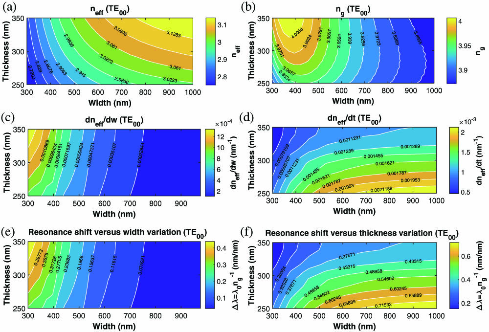
    Fig. 2. Finite difference eigen-mode (FDE) calculations for (a) effective index (neff), (b) group index (ng), (c) effective index change versus width (dneff/dw), (d) effective index change versus thickness (dneff/dt), (e) wavelength shift versus width (Δλ0/dw), (f) wavelength shift versus thickness (Δλ0/dt).
    (a) 3D schematic of the heterogeneous III–V/Si MOSCAP tuner, (b) simulated TE optical mode for a HfO2 dielectric interface, and (c) TEM image of a GaAs/dielectric/Si interface as an example.
    Fig. 3. (a) 3D schematic of the heterogeneous III–V/Si MOSCAP tuner, (b) simulated TE optical mode for a HfO2 dielectric interface, and (c) TEM image of a GaAs/dielectric/Si interface as an example.
    Simulated refractive index change and FCA losses for (a) n−GaAs/Al2O3/p−Si, and (b) n−GaAs/HfO2/p−Si for gap thicknesses of 5, 10, 15, 20, and 25 nm. Layer doping: n-GaAs (3×1018 cm−2), n−Al0.20Ga0.80As (3×1018 cm−2), Si (5×1016 cm−2).
    Fig. 4. Simulated refractive index change and FCA losses for (a) nGaAs/Al2O3/pSi, and (b) nGaAs/HfO2/pSi for gap thicknesses of 5, 10, 15, 20, and 25 nm. Layer doping: n-GaAs (3×10¹⁸  cm2), nAl0.20Ga0.80As (3×10¹⁸  cm2), Si (5×10¹⁶  cm2).
    65 GHz (de-)interleaver transmission response with and without MOSCAP phase tuning for (a) second-order AMZI and (b) third-order AMZI.
    Fig. 5. 65 GHz (de-)interleaver transmission response with and without MOSCAP phase tuning for (a) second-order AMZI and (b) third-order AMZI.
    65 GHz (de-)interleaver transmission response with and without MOSCAP phase tuning for (a) one-ring RAMZI, (b) two-ring RAMZI, (c) three-ring RAMZI, and (d) two-channel coupled two-ring resonator.
    Fig. 6. 65 GHz (de-)interleaver transmission response with and without MOSCAP phase tuning for (a) one-ring RAMZI, (b) two-ring RAMZI, (c) three-ring RAMZI, and (d) two-channel coupled two-ring resonator.
    Microscope images of various (de-)interleavers: (a) second-order AMZI; (b) third-order AMZI; (c)–(e) one-, two-, three-ring-assisted AMZIs; and (f) second-order cascaded rings.
    Fig. 7. Microscope images of various (de-)interleavers: (a) second-order AMZI; (b) third-order AMZI; (c)–(e) one-, two-, three-ring-assisted AMZIs; and (f) second-order cascaded rings.
    (a) Microscope image of angled III–V/Si test structures and cutback loss measurements for evaluating III–V/Si transition losses, (b) image of MOSCAP MZI structure for evaluating phase tuning efficiency and optical response as a function of bias voltage.
    Fig. 8. (a) Microscope image of angled III–V/Si test structures and cutback loss measurements for evaluating III–V/Si transition losses, (b) image of MOSCAP MZI structure for evaluating phase tuning efficiency and optical response as a function of bias voltage.
    Measured response of second-order MOSCAP AMZI (de-)interleaver with (a) un-corrected phase and (b) corrected phase with Vdelay1=−1 V.
    Fig. 9. Measured response of second-order MOSCAP AMZI (de-)interleaver with (a) un-corrected phase and (b) corrected phase with Vdelay1=1  V.
    Measured response of third-order MOSCAP AMZI (de-)interleaver with (a) un-corrected phase and (b) corrected phase with Vdelay1=0.3 V, Vdelay2=1 V, Vdelay3=0.1 V.
    Fig. 10. Measured response of third-order MOSCAP AMZI (de-)interleaver with (a) un-corrected phase and (b) corrected phase with Vdelay1=0.3  V, Vdelay2=1  V, Vdelay3=0.1  V.
    Measured response of one-ring-assisted MOSCAP AMZI (de-)interleaver with (a) un-corrected phase and (b) corrected phase at Vring1=0 V, Vdelay=−2 V. Measured response of two-ring-assisted MOSCAP AMZI (de-)interleaver with (c) un-corrected phase and (d) corrected phase at Vring1=0 V, Vring2=0 V, Vdelay=−2 V. Measured response of three-ring-assisted MOSCAP AMZI (de-)interleaver with (e) un-corrected phase and (f) corrected phase at Vring1=0 V, Vring2=0 V, Vring2=0 V, Vdelay=−3 V.
    Fig. 11. Measured response of one-ring-assisted MOSCAP AMZI (de-)interleaver with (a) un-corrected phase and (b) corrected phase at Vring1=0  V, Vdelay=2  V. Measured response of two-ring-assisted MOSCAP AMZI (de-)interleaver with (c) un-corrected phase and (d) corrected phase at Vring1=0  V, Vring2=0  V, Vdelay=2  V. Measured response of three-ring-assisted MOSCAP AMZI (de-)interleaver with (e) un-corrected phase and (f) corrected phase at Vring1=0  V, Vring2=0  V, Vring2=0  V, Vdelay=3  V.
    AuthorsDevice TypeMaterialWave. (μm)Sep. (GHz)XT (dB)IL (dB)Tuning Pow. (mW)
    Q. Deng2nd-order AMZISi1.551838−150.40
    A. Rizzo [16]1-ring RAMZISi1.55400−15<1N/A
    S. Lai [41]SCOWSi1.55100−2080
    J. F. Song [19]1-ring RAMZISi1.55178−22825.5
    N. Zhou [18]MZI-SLMSi1.5556N/A<123
    J. F. Song [42]1-ring RAMZISi1.551250−7 to −10100
    J. F. Song [43]1-ring RAMZISi1.55250<1080
    L. W. Luo [14]3-ring RAMZISi1.55120−2085
    M. Cherchi [44]2nd-order AMZISi1.551875−2230
    M. Cherchi [45]1-ring RAMZISi1.55125−9 to −1830
    X. Jiang [46]MZI-SLMSi1.55123−20<1N/A
    This work2nd-order AMZIIIIV/Al2O3/Si1.3165−22 to −1520.000083
    This work3rd-order AMZIIIIV/Al2O3/Si1.3165−32 to −221.40.000053
    This work1-ring RAMZIIIIV/Al2O3/Si1.3165−27 to −161.80.000010
    This work2-ring RAMZIIIIV/Al2O3/Si1.3165−22 to −212.00.00722
    This work3-ring RAMZIIIIV/Al2O3/Si1.3165−20 to −184.40.000034
    Table 1. Complete Survey of State-of-the-Art DWDM Si (De-)interleavers
    DesignΔL (μm)c1c2c3c4
    2nd-order AMZI610.50.500.290.08
    3rd-order AMZI610.50.500.190.190.025
    Table 2. Design Summary of III–V/Si MOSCAP Nth-Order AMZI (De-)interleavers
    DesignLring (μm)κr1κr2κr3c0c1
    1-ring RAMZI12000.890.500.50
    2-ring RAMZI12000.970.620.500.50
    3-ring RAMZI12000.960.680.250.500.50
    Table 3. Design Summary of III–V/Si MOSCAP One-, Two-, Three-ring RAMZI (De-)interleavers
    Design NameSi Doping (cm3)Gate Type
    Design 14 × 1016Al2O3 (6 nm)
    Design 25 × 1017HfO2/Al2O3 (10/3 nm)
    Design 3u.i.d.HfO2/Al2O3 (5.4/3 nm)
    Table 4. Fabricated Platform Variations
    Stanley Cheung, Geza Kurczveil, Yingtao Hu, Mingye Fu, Yuan Yuan, Di Liang, Raymond G. Beausoleil. Ultra-power-efficient heterogeneous III–V/Si MOSCAP (de-)interleavers for DWDM optical links[J]. Photonics Research, 2022, 10(2): A22
    Download Citation