
Shuailong Zhang, Mohamed Elsayed, Ran Peng, Yujie Chen, Yanfeng Zhang, Steven L. Neale, Aaron R. Wheeler, "Influence of light pattern thickness on the manipulation of dielectric microparticles by optoelectronic tweezers," Photonics Res. 10, 550 (2022)
- Photonics Research
- Vol. 10, Issue 2, 550 (2022)
Abstract
1. INTRODUCTION
Optoelectronic tweezer (OET) is an optical micromanipulation technology that relies on optically induced-dielectrophoresis (ODEP) force for the control of micro-/nano-scale objects [1–5]. Based on light patterned electric fields, OET is capable of exerting pico-to-nano Newton manipulation forces [6,7], and is well suited for parallel and independent control of multiple objects [1,3,8,9]. Because of these outstanding micromanipulation capabilities, OET has been widely used to manipulate and assemble bio-analytes and molecules [10–12], cells of different species [13–20], nano-/microparticles [8,21–26], electronic/photonic components [27–33], and microrobots [9], thus offering a powerful scientific tool to investigate the microscopic world for physical, chemical, and biological studies. More recently, OET technology has been successfully commercialized and used in the biopharmaceutical industry for antibody discovery and cell therapy development [34], demonstrating the prospect of this technology in both research and industrial settings.
In an OET system, the light pattern is a key factor that influences the moving behavior of the controlled micro-objects. Previous studies have shown that both the wavelength and optical intensity of light patterns can influence the performance of OET for particle manipulation [35,36]. However, for a given OET system with a fixed light source, there is little room to adjust the properties of the light to optimize the performance of the ODEP forces that enable OET applications. Therefore, in this work, we explored a more readily modifiable variable—the thickness of the projected light pattern—to study the effects of this variable on the movement of microparticles. Simulations in COMSOL Multiphysics (COMSOL Inc., USA) were carried out to clarify the experimental results and provide insights to the physical mechanisms. It was demonstrated that thicker light patterns can induce stronger electric field gradients in the horizontal plane, exerting stronger horizontal DEP forces and thus a higher moving velocity for the microparticles. However, light patterns beyond a certain thickness can increase the DEP force in the vertical plane, making the microparticles escape from the OET trap at a lower horizontal moving velocity. Therefore, these two physical mechanisms should be considered when choosing the right parameters for light patterns to achieve optimal OET performance for micromanipulation. We show that this observation generally holds true for microparticles that experience negative DEP, but note that the relationship will be different for objects that experience positive DEP.
2. RESULTS AND DISCUSSION
Shown in Fig. 1(a) is a schematic of an OET device, comprising two plates. The top plate is an indium tin oxide (ITO)-coated glass slide; the bottom plate is also an ITO-coated glass slide, but with an additional photoconductive layer of hydrogenated-amorphous-silicon (a-Si:H) deposited onto it. The two plates were mounted together via a 150-μm-thick spacer to form a microchamber, in which the micromanipulation was performed. When a bias voltage is applied between the two plates and a light pattern is projected on the a-Si:H layer, a non-uniform electric field is generated in the liquid microchamber, which interacts with the micro-objects and produces DEP forces. If the micro-object is more polarizable than the surrounding medium [i.e., the real part of the Clausius–Mossotti (CM) factor is above zero], it will be attracted to the illuminated region due to a positive DEP force; if the micro-object is less polarizable than the surrounding medium (i.e., the real part of the CM factor is below zero), it will be repelled from the illuminated region due to a negative DEP force [37]. In this work, 10 μm diameter spherical polystyrene microbeads (Polysciences Inc., USA) were used, which were suspended in deionized water containing Tween 20 (0.05% volume fraction) and pipetted into the microchamber of the OET device. The OET device was driven by an AC potential (10Vpp 20 kHz square wave). On applying the AC voltage, the polystyrene beads were repelled by the illuminated region due to the negative DEP force, allowing the use of hollow light patterns consisting of illuminated and dark regions to move and rotate the beads, as shown in Fig. 1(b) and
Sign up for Photonics Research TOC. Get the latest issue of Photonics Research delivered right to you!Sign up now
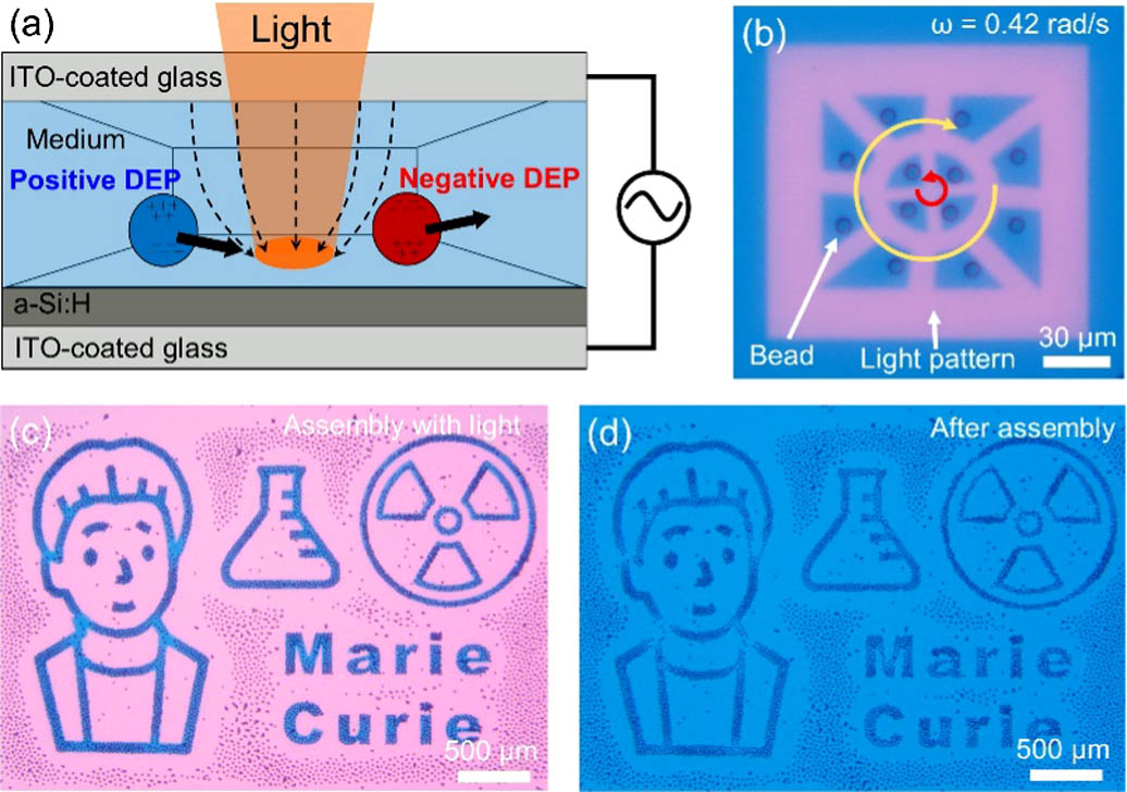
Figure 1.(a) Schematic of an OET device, in which microparticles are manipulated via positive or negative DEP forces. (b) Video frame showing the use of dynamic light patterns to move/rotate multiple 10 μm polystyrene microbeads at an angular velocity of 0.42 rad/s. Red and yellow arrows represent the counterclockwise and clockwise rotational directions of the microbeads in the central and surrounding regions, respectively. Regions with red color represent the illuminated region, and regions with blue color represent the dark region. See
To investigate the influence of the light pattern on the ability to move microparticles, a single 10-μm-diameter bead was trapped by “doughnut”-shaped light patterns with a fixed inner diameter at 80 μm but different ring thicknesses, as shown in Figs. 2(a)–2(c) and
![]()
Figure 2.(a)–(c) Microscope images of a 10 μm polystyrene microbead trapped by doughnut-shaped light patterns with the same inner diameter but different ring thicknesses (i.e., 5 μm, 20 μm, and 110 μm), and moving at 180 μm/s, 430 μm/s, and 320 μm/s, respectively. See
For each doughnut ring thickness evaluated, the maximum moving velocity of the bead was measured by gradually increasing the speed of the motorized stage, observing the velocity at which the bead fell out of the trap (see
To probe the phenomenon of reduced force found for thick doughnut rings and to clarify the physical mechanism for the observed experimental results, simulations were carried out in COMSOL Multiphysics using the AC/DC module (COMSOL Inc., Burlington, MA, accessed via license obtained through CMC Microsystems, Kingston, Canada) [6–9]. The model length (
Shown in Figs. 3(a) and 3(b) are the heat maps of the simulated electric potential and electric field distribution (i.e., cross-sectional view of an OET device). As shown, there is a big potential change at the edge of the light pattern resulting in a region of strong electric field with sharp field variation. This is caused by the difference in conductivity between the illuminated and dark a-Si:H surfaces. Since the bead reaches its maximum velocity at the edge of the light pattern, it is here that we investigate the DEP manipulation force exerted on the bead. Based on classic DEP theory for spherical microparticles [37], the DEP force is given by
![]()
Figure 3.Plots of (a) simulated electric potential, and (b) simulated electric field for an OET trap formed by illuminating a doughnut-shaped light pattern on the photoconductive layer of an OET device. The simulated electric potential and electric field are plotted in heat maps (blue, low; red, high). The inset in (b) is a magnified view of the main-panel data in the dashed square. Simulated gradients of electric field square (c) along
To test the universality of the physical mechanism, rectangular-shaped light patterns with fixed length at 270 μm but different thicknesses were used to manipulate a microbead, as shown in Figs. 4(a)–4(c) and
![]()
Figure 4.(a)–(c) Microscope images of a 10 μm polystyrene microbead moved by rectangular-shaped light patterns with the same length but different thicknesses (i.e., 5 μm, 25 μm, and 110 μm), and moving at 35 μm/s, 125 μm/s, and 90 μm/s, respectively. The red arrow represents the moving direction. See
Finally, motivated by the recent report of OET-driven micromachines formed from circular micro-gear structures [47], we applied similar techniques to evaluate effects on micro-gears, depicted in Fig. 5(a). The micro-gears used here are formed from SU8 (Kayaku Advanced Materials) and are fabricated using standard photolithography techniques [9]. They have a diameter of 200 μm and a height of 60 μm, much larger than the 10-μm-diameter polystyrene microbeads described above. Regardless, micro-gears can be made to move at different velocities using doughnut-shaped light patterns with different ring thicknesses, as shown in Figs. 5(b)–5(d) and
![]()
Figure 5.(a) SEM image of a micro-gear. (b)–(d) Microscope images of a micro-gear trapped by doughnut-shaped light patterns with the same inner diameter but different ring thicknesses (i.e., 10 μm, 40 μm, and 110 μm), and moving at 300 μm/s, 410 μm/s, and 350 μm/s, respectively. The red arrow represents the moving direction. See
The asymmetry of the particles in micro-gear experiments (relative to the symmetric spherical beads described above) provides additional substantiation of the “vertical DEP” hypothesis. Shown in Figs. 5(f)–5(h) are microscope images of a micro-gear escaping from a doughnut-shaped light pattern (from
For micro-objects that experience positive DEP, such as metallic microparticles [6], we did not observe the phenomenon reported in this work. The main reason is that microparticles experiencing positive DEP forces will also experience positive vertical DEP forces, which pull down the microparticles toward the surface of the OET bottom plate instead of lifting them up. In addition, we find in the experiments that different inner diameters of doughnut-shaped light patterns can significantly influence the maximum velocity of the particle experiencing negative DEP. However, this is likely due to a different mechanism. For light patterns with fixed pattern thicknesses but different inner diameters, the interactive interface/region between the light boundary and the microparticle is different (due to different curvature of the boundary). For example, if the inner diameter of the light pattern is small enough (with a size similar to the particle), the doughnut-shaped light pattern will function like a solid circular light pattern and start to repel the particle, making it escape from the central dark region, and the moving velocity is not measurable. These results demonstrate the important and complex nature of light pattern layout on the behaviors of micro-objects under OET manipulation, which normally involves several physical mechanisms for different circumstances and is worthy of continuing study in the future.
3. CONCLUSION
In conclusion, we studied the influence of light pattern thickness on the ability to move microparticles and micro-gears manipulated by OET. The experiments were supported by numerical simulations. It was found that the light pattern thickness can influence both horizontal and vertical DEP forces, leading to first an increase and then a decrease of the maximum velocity achievable by the micro-object as the light pattern thickness increases. This result provides important insight about the optimization of light pattern parameters to achieve better OET performance for micromanipulation applications. In particular, users who employ negative DEP in their experiments should consider both horizontal and vertical DEP forces when selecting the appropriate light pattern parameters to increase the moving velocities of micro-objects and exert stronger manipulation forces, which is important for improving OET performance for many micromanipulation applications.
4. METHODS
The OET setup comprises a digital mirror device (DMD) pattern illuminator (Mightex Polygon 1000, 625 nm, 1100 mW LED source) interfaced with an upright optical microscope (Nikon Eclipse Ni-E microscope integrated with Märzhäuser Scan Plus 130-85 motorized stage and LW scientific MiniVID CMOS camera). The average power density of projected light patterns remains constant at
Suspensions of polystyrene microparticles (10 μm diameter, Polysciences) were formed at 106 to
Acknowledgment
Acknowledgment. The authors acknowledge the support from the Centre for Nanostructure Imaging at the Department of Chemistry, University of Toronto, for assistance in collecting SEM images, and the Centre for Research and Applications in Fluidic Technologies (CRAFT) for assistance in micro-gear fabrication. A. R. W. acknowledges the Canada Research Chair (CRC) program.
References
[1] P. Y. Chiou, A. T. Ohta, M. C. Wu. Massively parallel manipulation of single cells and microparticles using optical images. Nature, 436, 370-372(2005).
[2] M. C. Wu. Optoelectronic tweezers. Nat. Photonics, 5, 322-324(2011).
[3] M. Woerdemann, C. Alpmann, M. Esseling, C. Denz. Advanced optical trapping by complex beam shaping. Laser Photon. Rev., 7, 839-854(2013).
[4] Y. Huang, Z. Liang, M. Alsoraya, J. Guo, D. Fan. Light-gated manipulation of micro/nanoparticles in electric fields. Adv. Intell. Syst., 2, 1900127(2020).
[5] H. Hwang, J. K. Park. Optoelectrofluidic platforms for chemistry and biology. Lab Chip, 11, 33-47(2011).
[6] S. Zhang, Y. Liu, J. Juvert, P. Tian, J. C. Navaro, J. M. Cooper, S. L. Neale. Use of optoelectronic tweezers in manufacturing accurate solder bead positioning. Appl. Phys. Lett., 109, 221110(2016).
[7] S. Zhang, J. Juvert, J. M. Cooper, S. L. Neale. Manipulating and assembling metallic beads with optoelectronic tweezers. Sci. Rep., 6, 32840(2016).
[8] S. Zhang, Y. Zhai, R. Peng, M. Shayegannia, A. G. Flood, J. Qu, X. Liu, N. P. Kherani, A. R. Wheeler. Assembly of topographical micropatterns with optoelectronic tweezers. Adv. Opt. Mater., 7, 1900669(2019).
[9] S. Zhang, E. Y. Scott, J. Singh, Y. Chen, Y. Zhang, M. Elsayed, M. D. Chamberlain, N. Shakiba, K. Adams, S. Yu, C. M. Morshead, P. W. Zandstra, A. R. Wheeler. The optoelectronic microrobot: a versatile toolbox for micromanipulation. Proc. Natl. Acad. Sci. USA, 116, 14823-14828(2019).
[10] D. Han, J. K. Park. Optoelectrofluidic enhanced immunoreaction based on optically-induced dynamic AC electroosmosis. Lab Chip, 16, 1189-1196(2016).
[11] D. Han, J. K. Park. Microarray-integrated optoelectrofluidic immunoassay system. Biomicrofluidics, 10, 034106(2016).
[12] Y. H. Lin, C. M. Chang, G. B. Lee. Manipulation of single DNA molecules by using optically projected images. Opt. Express, 17, 15318-15329(2009).
[13] Y. Zhang, J. Zhao, H. Yu, P. Li, W. Liang, Z. Liu, G. B. Lee, L. Liu, W. J. Li, Z. Wang. Detection and isolation of free cancer cells from ascites and peritoneal lavages using optically induced electrokinetics (OEK). Sci. Adv., 6, eaba9628(2020).
[14] S. Zhang, N. Shakiba, Y. Chen, Y. Zhang, P. Tian, J. Singh, M. D. Chamberlain, M. Satkauskas, A. G. Flood, N. P. Kherani, S. Yu, P. W. Zandstra, A. R. Wheeler. Patterned optoelectronic tweezers: a new scheme for selecting, moving, and storing dielectric particles and cells. Small, 14, 1803342(2018).
[15] S. Xie, X. Wang, N. Jiao, S. Tung, L. Liu. Programmable micrometer-sized motor array based on live cells. Lab Chip, 17, 2046-2053(2017).
[16] A. T. Ohta, M. Garcia, J. K. Valley, L. Banie, H. Y. Hsu, A. Jamshidi, S. L. Neale, T. Lue, M. C. Wu. Motile and non-motile sperm diagnostic manipulation using optoelectronic tweezers. Lab Chip, 10, 3213-3217(2010).
[17] S. B. Huang, M. H. Wu, Y. H. Lin, C. H. Hsieh, C. L. Yang, H. C. Lin, C. P. Tseng, G. B. Lee. High-purity and label-free isolation of circulating tumor cells (CTCs) in a microfluidic platform by using optically-induced-dielectrophoretic (ODEP) force. Lab Chip, 13, 1371-1383(2013).
[18] L. Y. Ke, Z. K. Kuo, Y. S. Chen, T. Y. Yeh, M. Dong, H. W. Tseng, C. H. Liu. Cancer immunotherapy μ-environment LabChip: taking advantage of optoelectronic tweezers. Lab Chip, 18, 106-114(2018).
[19] Y. Yang, Y. Mao, K. S. Shin, C. O. Chui, P. Y. Chiou. Self-locking optoelectronic tweezers for single-cell and microparticle manipulation across a large area in high conductivity media. Sci. Rep., 6, 22630(2016).
[20] A. H. Jeorrett, S. L. Neale, D. Massoubre, E. Gu, R. K. Henderson, O. Millington, K. Mathieson, M. D. Dawson. Optoelectronic tweezers system for single cell manipulation and fluorescence imaging of live immune cells. Opt. Express, 22, 1372-1380(2014).
[21] A. Jamshidi, S. L. Neale, K. Yu, P. J. Pauzauskie, P. J. Schuck, J. K. Valley, H.-Y. Hsu, A. T. Ohta, M. C. Wu. Nanopen: dynamic, low-power, and light-actuated patterning of nanoparticles. Nano Lett., 9, 2921-2925(2009).
[22] S. J. Lin, S. H. Hung, J. Y. Jeng, T. F. Guo, G. B. Lee. Manipulation of micro-particles by flexible polymer-based optically-induced dielectrophoretic devices. Opt. Express, 20, 583-592(2012).
[23] M. B. Lim, R. G. Felsted, X. Zhou, B. E. Smith, P. J. Pauzauskie. Patterning of graphene oxide with optoelectronic tweezers. Appl. Phys. Lett., 113, 031106(2018).
[24] S. Liang, Y. Cao, Y. Dai, F. Wang, X. Bai, B. Song, C. Zhang, C. Gan, F. Arai, L. Feng. A versatile optoelectronic tweezer system for micro-objects manipulation: transportation, patterning, sorting, rotating and storage. Micromachines, 12, 271(2021).
[25] S. Zhang, W. Li, M. Elsayed, P. Tian, A. W. Clark, A. R. Wheeler, S. L. Neale. Size-scaling effects for microparticles and cells manipulated by optoelectronic tweezers. Opt. Lett., 44, 4171-4174(2019).
[26] M. A. Zaman, P. Padhy, Y. T. Cheng, L. Galambos, L. Hesselink. Optoelectronic tweezers with a non-uniform background field. Appl. Phys. Lett., 117, 171102(2020).
[27] A. Jamshidi, P. J. Pauzauskie, P. J. Schuck, A. T. Ohta, P. Y. Chiou, J. Chou, P. Yang, M. C. Wu. Dynamic manipulation and separation of individual semiconducting and metallic nanowires. Nat. Photonics, 2, 86-89(2008).
[28] Y. H. Lin, K. S. Ho, C. T. Yang, J. H. Wang, C. S. Lai. A highly flexible platform for nanowire sensor assembly using a combination of optically induced and conventional dielectrophoresis. Opt. Express, 22, 13811-13824(2014).
[29] H. Hwang, D. Han, Y. J. Oh, Y. K. Cho, K. H. Jeong, J. K. Park. In situ dynamic measurements of the enhanced SERS signal using an optoelectrofluidic SERS platform. Lab Chip, 11, 2518-2525(2011).
[30] M. B. Lim, J. L. Hanson, L. Vandsburger, P. B. Roder, X. Zhou, B. E. Smith, F. S. Ohuchi, P. J. Pauzauskie. Copper-and chloride-mediated synthesis and optoelectronic trapping of ultra-high aspect ratio palladium nanowires. J. Mater. Chem. A, 6, 5644-5651(2018).
[31] S. Zhang, Y. Liu, Y. Qian, W. Li, J. Juvert, P. Tian, J. C. Navarro, A. W. Clark, E. Gu, M. D. Dawson, J. M. Cooper, S. L. Neale. Manufacturing with light-micro-assembly of opto-electronic microstructures. Opt. Express, 25, 28838-28850(2017).
[32] M. C. Tien, A. T. Ohta, K. Yu, S. L. Neale, M. C. Wu. Heterogeneous integration of InGaAsP microdisk laser on a silicon platform using optofluidic assembly. Appl. Phys. A, 95, 967-972(2009).
[33] J. Juvert, S. Zhang, I. Eddie, C. J. Mitchell, G. T. Reed, J. S. Wilkinson, A. Kelly, S. L. Neale. Micromanipulation of InP lasers with optoelectronic tweezers for integration on a photonic platform. Opt. Express, 24, 18163-18175(2016).
[34] https://www.berkeleylights.com/. https://www.berkeleylights.com/
[35] W. Liang, S. Wang, Z. Dong, G. B. Lee, W. J. Li. Optical spectrum and electric field waveform dependent optically-induced dielectrophoretic (ODEP) micro-manipulation. Micromachines, 3, 492-508(2012).
[36] J. K. Valley, A. Jamshidi, A. T. Ohta, H. Y. Hsu, M. C. Wu. Operational regimes and physics present in optoelectronic tweezers. J. Microelectromech. Syst., 17, 342-350(2008).
[37] R. Pethig. Dielectrophoresis: status of the theory, technology, and applications. Biomicrofluidics, 4, 022811(2010).
[38] S. L. Neale, M. Mazilu, J. I. B. Wilson, K. Dholakia, T. F. Krauss. The resolution of optical traps created by light induced dielectrophoresis (LIDEP). Opt. Express, 15, 12619-12626(2007).
[39] N. Liu, Y. Lin, Y. Peng, L. Xin, T. Yue, Y. Liu, C. Ru, S. Xie, L. Dong, H. Pu, H. Chen, W. J. Li, Y. Sun. Automated parallel electrical characterization of cells using optically-induced dielectrophoresis. IEEE Trans. Autom. Sci. Eng., 17, 1084-1092(2020).
[40] S. Zhang, A. Nikitina, Y. Chen, Y. Zhang, L. Liu, A. G. Flood, J. Juvert, M. D. Chamberlain, N. P. Kherani, S. L. Neale, A. R. Wheeler. Escape from an optoelectronic tweezer trap: experimental results and simulations. Opt. Express, 26, 5300-5309(2018).
[41] W. Liang, L. Liu, H. Zhang, Y. Wang, W. J. Li. Optoelectrokinetics-based microfluidic platform for bioapplications: a review of recent advances. Biomicrofluidics, 13, 051502(2019).
[42] Y. H. Lin, G. B. Lee. Optically induced flow cytometry for continuous microparticle counting and sorting. Biosens. Bioelectron., 24, 572-578(2008).
[43] Y. S. Chen, C. P. K. Lai, C. Chen, G. B. Lee. Isolation and recovery of extracellular vesicles using optically-induced dielectrophoresis on an integrated microfluidic platform. Lab Chip, 21, 1475-1483(2021).
[44] C. Witte, J. Reboud, J. M. Cooper, S. L. Neale. Channel integrated optoelectronic tweezer chip for microfluidic particle manipulation. J. Micromech. Microeng., 30, 045004(2020).
[45] T. K. Chiu, W. P. Chou, S. B. Huang, H. M. Wang, Y. C. Lin, C. H. Hsieh, M. H. Wu. Application of optically-induced-dielectrophoresis in microfluidic system for purification of circulating tumour cells for gene expression analysis-cancer cell line model. Sci. Rep., 6, 32851(2016).
[46] W. P. Chou, H. M. Wang, J. H. Chang, T. K. Chiu, C. H. Hsieh, C. J. Liao, M. H. Wu. The utilization of optically-induced-dielectrophoresis (ODEP)-based virtual cell filters in a microfluidic system for continuous isolation and purification of circulating tumour cells (CTCs) based on their size characteristics. Sens. Actuators B Chem., 241, 245-254(2017).
[47] S. Zhang, M. Elsayed, R. Peng, Y. Chen, Y. Zhang, J. Peng, W. Li, M. D. Chamberlain, A. Nikitina, S. Yu, X. Liu, S. L. Neale, A. R. Wheeler. Reconfigurable multi-component micromachines driven by optoelectronic tweezers. Nat. Commun., 12, 5349(2021).


Set citation alerts for the article
Please enter your email address

© Copyright 2018-2021 | Chinese Laser Press. All Rights Reserved 沪ICP备15018463号-20