
Hao Chen, Xiuming Dou, Kun Ding, Baoquan Sun. Electrically driven uniaxial stress device for tuning in situ semiconductor quantum dot symmetry and exciton emission in cryostat[J]. Journal of Semiconductors, 2019, 40(7): 072901
- Journal of Semiconductors
- Vol. 40, Issue 7, 072901 (2019)
Abstract
1. Introduction
Single photon and entangled photon pairs emitters on demand are a major building block for quantum computation and communication[
2. Experimental setup
2.1. Design of the electrically driven uniaxial stress device
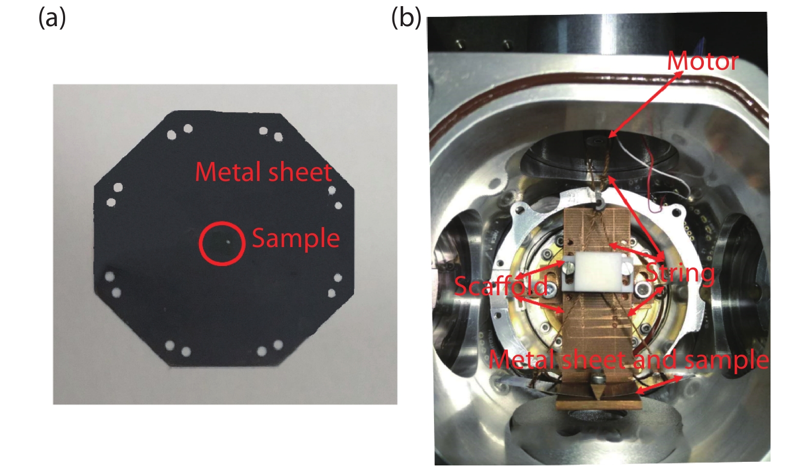
In this article, we report on a technique of applied uniaxial stress on the sample at low temperature. As shown in Fig. 1(a), firstly, the sample is needed to be prepared into a thin film and transferred it onto the center of the polished metal sheet, where the sample film is absorbed on the metal sheet by van der Waals force. Two pairs of round holes on the edge of the sheet along with diagonal line are used to fix the string and stretch the metal sheet. In this case the uniaxial stress can be applied in four directions of the sample. Second, the metal sheet is fixed on the scaffold with the help of a wedge and two screws, as shown in Fig. 1(b). A hook is used to hook two strings. The other end of the hook is connected to a slider, forming a system similar to a fixed pulley. The piezoelectric motor connected with the slider is employed to bend metal sheet and apply uniaxial stress on the sample. In addition, in order to keep piezoelectric motor working normally, we fix it on the side wall of the cryostat for its working at room temperature. In this case, the designed device has an advantage of the sample at low temperature and piezoelectric motor at room temperature, separately.
![]()
Figure 1.(Color online) (a) Photograph of a polished metal sheet with a sample on the center, where metal sheet as a flexible substrate of absorbed sample. (b) Photograph of the electrically driven uniaxial stress device fixed on the cold chamber of cryostat.
2.2. Temperature calibration
Note that the lowest temperature of the platform temperature of cryostat displays 4 K in our cryostat. However, this temperature is not an actual temperature of the sample on the device. To calibrate the sample temperature, small particles of Ruby are adhered to the metal sheet. The exact temperature of the sample on the metal sheet can be obtained by measuring the intensity ratio R2/R1 of the Ruby photoluminescence (PL) peaks R2 and R1. A small piece of Ruby is stuck on the platform of the cryostat, then the intensity ratio R2/R1 as a function of temperature is obtained, shown in Fig. 2(a). Fig. 2(b) shows the PL spectrum of ruby on the metal sheet at a temperature of about 15 K. It is found that with applying tension or release stress, PL peak wavelength of ruby remains to be unchanged, indicating that the temperature of the metal sheet is stable.
![]()
Figure 2.(Color online) (a) PL intensity ratio
2.3. Stress calibration
Note that uniaxial tensile stress-dependent PL peak shift of GaAs has been reported, corresponding PL peak red shift at a rate of 33 μeV/MPa[
![]()
Figure 3.(Color online) (a) Stress-dependent spectra of GaAs at 15 K, measured for applied uniaxial tensile stress from zero to 879.5 MPa. (b) PL peak energy as a function of tensile (black solid squares) and release (red solid circles) stresses, respectively.
3. Several applications of the uniaxial stress device
In the following we will measure the PL spectral shifts of exciton (X), biexciton (XX), and charged (X*) exciton emissions, as well as charged exciton decay time and exciton FSS of InAs/GaAs QDs by using developed uniaxial stress tuning device at 15 K. In addition, band edge PL shift of two-dimensional thin film materials is also measured.
3.1. In situ tuning exciton, biexciton and charged exciton emissions
The studied InAs/GaAs QD samples were grown on a (001) GaAs substrate by molecular beam epitaxy (MBE). It consists of a 200 nm GaAs buffer layer, a 100 nm AlAs sacrificial layer, a 30 nm GaAs layer, a InAs QD layer, and a 100 nm GaAs cap layer. After etching away the AlAs sacrificed layer, we transferred a thin film with a thickness of 130 nm GaAs containing InAs QDs onto the polished metal sheet (see Fig. 1(a)), while the sample’s (110) crystal orientation of GaAs at zero stress was aligned along one of the applied uniaxial stress direction carefully.
The QDs was excited by a λ= 640 nm semiconductor laser. The excitation laser was focused to a spot with a diameter of ~2 μm on the sample using a microscope objective (NA: 0.45). The PL was collected using the same objective, and measured using a 0.5 m focal length monochrometer equipped with a silicon charge-coupled device.
Fig. 4(a) presents the measured PL spectra of X, XX and X* at 15 K under different uniaxial stresses. It can be seen that all the exciton PL peaks show a kind of red shift as the stress increases from 0 to 717.6 MPa. The corresponding red shift of PL peak wavelength is approximately 7 nm, which can be tuned in situ at 15 K continuously. We also found that the PL intensities show a decrease with increasing stress. Fig. 4(b) shows a plot of PL peak energies as function of applied stress. By linearly fit to data, the obtained stress coefficients for X, XX and X* are –20.26, –18.93 and –20.19 μeV/MPa, respectively.
![]()
Figure 4.(Color online) (a) PL spectra for X*, X and XX in QD measured under the tensile stress of 0, 104.4, 201.2, 321.7, 391.9, 500.7, 614.2 and 717.6 MPa, respectively. (b) The obtained stress coefficients for X*, X and XX are –20.19, –20.26 and –18.93
3.2. Radiation lifetime and FSS under applied stress
The QD PL decay curve is measured by using silicon avalanche photodiode (APD) and time-correlated single photon counting (TCSPC) setup with an instrument response time of ~ 300 ps at 15 K.
Note that two non-degenerates bright X emissions correspond to two mutually perpendicular linearly polarized photon emissions[
![]()
Figure 5.(Color online) (a) FSS change of the exciton in single QD as a function of strain applied along (100) and (010) directions, respectively. (b) Charged exciton decay times of single QD as a function of strain applied along (100) and (010) directions, respectively.
3.3. Realizing the entanglement condition of time reordering
An alternative proposal to generate entangled photon pairs from QDs, without any fundamental requirements on the FSS to be smaller (instead, a larger FSS may be better) than the radiative line width, is the so-called time reordering scheme[
![]()
Figure 6.(Color online) (a)–(d) Stress-dependent spectra of single QD at 15 K. As shown in (b) and (d), PL spectra of the horizontal (red lines) and vertical (black lines) polarized components of exciton and biexciton overlap at the stresses of 491.8 and 960.4 MPa, respectively. At 698.3 MPa as shown in (c), across generation color coincidence for XX and X transition energies is achieved. (e)–(h) Level schemes showing the XX-X cascade emissions accordingly.
3.4. Tuning PL spectra of thin film materials
The uniaxial stress device can also be used to tune band edge PL of two-dimensional thin film materials at low temperature. Here monolayer MoS2 is chosen for its stress-independent PL measurements. Monolayer MoS2 is first exfoliated onto a Si/SiO2 substrate. Then the target monolayer is transferred into a polished metal sheet using poly(methyl methacrylate) (PMMA) as the transfer medium. After transferring, the PMMA is removed. Fig. 7 show the measured PL spectra under different stresses at 15 K, indicating PL peak red shift as increasing stress.
![]()
Figure 7.(Color online) Stress-dependent PL spectra of monolayer MoS2 at 15 K, corresponding motor precession from 0 to 330 000 steps.
4. Summary
In summary, we have presented a technique for electrically driven uniaxial stress device which can be employed at low temperature. It enables us in situ tune exciton optical properties at 15 K with a single and convenient way. For the typical applications, stress-tuning optical properties of single InAs/Ga As QDs and band edge PL of monolayer MoS2 are presented.
Acknowledgements
This work was supported by the National Key Research and Development Program of China (Grant No. 2016YFA0301202) and the National Natural Science Foundation of China (Grant No. 61674135).
References
[1] R M Stevenson, A J Hudson, A J Bennett et al. Evolution of entanglement between distinguishable light states. Phys Rev Lett, 101, 170501(2008).
[2] W B Gao, P Fallahi, E Togan et al. Observation of entanglement between a quantum dot spin and a single photon. Nature, 491, 426(2012).
[3] P Lodahl, S Mahmoodian, S Stobbe. Interfacing single photons and single quantum dots with photonic nanostructures. Rev Mod Phys, 87, 347(2015).
[4] I Aharonovich, D Englund, M Toth. Solid-state single-photon emitters. Nat Photonics, 10, 631(2016).
[5] A Delteil, Z Sun, W B Gao et al. Generation of heralded entanglement between distant hole spins. Nat Phys, 12, 218(2016).
[6] P Senellart, G Solomon, A White. High-performance semiconductor quantum-dot single-photon sources. Nat Nanotechnol, 12, 1026(2017).
[7] H Wang, H Hu, T H Chung et al. On-demand semiconductor source of entangled photons which simultaneously has high fidelity, efficiency, and indistinguishability. Phys Rev Lett, 122, 113602(2019).
[8] J D Plumhof, R Trotta, A Rastelli et al. Experimental methods of post-growth tuning of the excitonic fine structure splitting in semiconductor quantum dots. Nanoscale Res Lett, 7, 336(2012).
[9] A J Bennett, M A Pooley, R M Stevenson et al. Electric-field-induced coherent coupling of the exciton states in a single quantum dot. Nat Phys, 6, 947(2010).
[10] M Ghali, K Ohtani, Y Ohno et al. Generation and control of polarization-entangled photons from GaAs island quantum dots by an electric field. Nat Commun, 3, 661(2012).
[11] R Trotta, E Zallo, C Ortix et al. Universal recovery of the energy-level degeneracy of bright excitons in InGaAs quantum dots without a structure symmetry. Phys Rev Lett, 109, 147401(2012).
[12] X F Wu, H Wei, X M Dou et al. In situ tuning biexciton antibinding-binding transition and fine-structure splitting through hydrostatic pressure in single InGaAs quantum dots. Europhys Lett, 107, 27008(2014).
[13] J Wang, M Gong, G C Guo et al. Eliminating the fine structure splitting of excitons in self-assembled InAs/GaAs quantum dots via combined stresses. Appl Phys Lett, 101, 2513(2012).
[14] X Dou, B Sun, B Wang et al. Photoluminescence energy and fine structure splitting in single quantum dots by uniaxial stress. Chin Phys Lett, 25, 1120(2008).
[15] R Keil, M Zopf, Y Chen et al. Solid-state ensemble of highly entangled photon sources at rubidium atomic transitions. Nat Commun, 8, 15501(2017).
[16] J Zhang, J S Wildmann, F Ding et al. High yield and ultrafast sources of electrically triggered entangled-photon pairs based on strain-tunable quantum dots. Nat Commun, 6, 10067(2015).
[17] F Ding, R Singh, J D Plumhof et al. Tuning the exciton binding energies in single self-assembled InGaAs/GaAs quantum dots by piezoelectric-induced biaxial stress. Phys Rev Lett, 104, 067405(2010).
[18] S B Desai, G Seol, J S Kang et al. Strain-induced indirect to direct bandgap transition in multi layer WSe2. Nano Lett, 14, 4592(2014).
[19] H J Conley, B Wang, J I Ziegler et al. Bandgap engineering of strained monolayer and bilayer MoS2. Nano Lett, 13, 3626(2013).
[20] M Cardona. Piezo-electroreflectance in Ge, GaAs, and Si. Phys Rev, 172, 816(1968).
[21] S Seidl, M Kroner et al. Effect of uniaxial stress on excitons in a self-assembled quantum dot. Appl Phys Lett, 88, 2513(2006).
[22] M Gong, W Zhang, G C Guo et al. exciton polarization, fine-structure splitting, and the asymmetry of quantum dots under uniaxial stress. Phys Rev Lett, 106, 227401(2011).
[23] W Xiong, X Xu, J W Luo et al. fundamental intrinsic lifetimes in semiconductor self-assembled quantum dots. Phys Rev Appl, 10, 044009(2018).
[24] F Troiani, C Tejedor. Entangled photon pairs from a quantum-dot cascade decay: The effect of time reordering. Phys Rev B, 78, 155305(2008).


Set citation alerts for the article
Please enter your email address

© Copyright 2018-2021 | Chinese Laser Press. All Rights Reserved 沪ICP备15018463号-20