Huixin Qi, Xiaoxiao Wang, Xiaoyong Hu, Qihuang Gong. Exceptional points in metasurface[J]. Infrared and Laser Engineering, 2020, 49(9): 20201029
Search by keywords or author
- Infrared and Laser Engineering
- Vol. 49, Issue 9, 20201029 (2020)
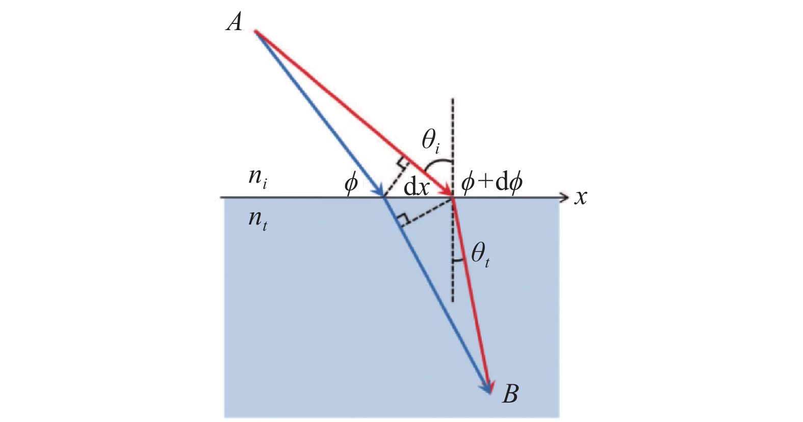
![Schematics used to derive the generalized Snell's law of refraction[14]](/richHtml/irla/2020/49/9/20201029/img_1.jpg)
Fig. 1. Schematics used to derive the generalized Snell's law of refraction[14]
![Real (imaginary) part of refractive index is an even (odd) function of the x axis[18]](/richHtml/irla/2020/49/9/20201029/img_2.jpg)
Fig. 3. Schematic representation of a generic two-level system composed of two coupled entities[21]
Fig. 4. Optical wave propagation when the system is excited at either channel 1 or channel 2 in a PT-symmetric system light propagates in a non-reciprocal manner both below and above threshold[22]
Fig. 5. Eigenvalues of coupled dual waveguide systems with the same gain/loss and the eigenvalue varies with the gain/loss coefficient. Real parts (“Re”, solid lines) and imaginary parts (“Im”, dashed lines) of the two normalized eigenvalues, and the position of the exceptional points[29]
Fig. 6. A parity-time-symmetric ternary micro-ring system with equidistantly spaced cavities. The side resonators experience balanced gain and loss whereas the middle one is neutral[24]
Fig. 7. Real parts (left) and the imaginary parts (right) of the eigenfrequencies of the ternary parity-time-symmetric system as a function of the normalized gain/loss contrast g /κ and the detuning ε /κ
Fig. 8. Photograph of PT symmetric metasurface composed of 300 nm thick silver (yellow or light gray) and lead (turquoise or dark gray) SRRs on silicon substrate [32]
Fig. 9. Schematic of PT symmetric metasurface with less lossy dipoles (blue) and more lossy dipoles (red) that is symmetric about y equals minus x
Fig. 10. Eigenpolarization states of transmission through an ideal PT symmetric metasurface when Gxy changes
Fig. 11. Schematic of the metasurface design. Each unit cell contains two strip antennas with thickness t =30 nm in the out-of-plane direction, lengths a 1=401.75 nm anda 2=435 nm, and widths w 1=50 nm and w 2=100 nm. Both antennas are free-standing, with a lattice periodd =600 nm
Fig. 12. Schematic of the metasurface unit cell geometry. The dimensions of each unit are set to L 1=L 3=30 μm, L 2=55 μm, L 4=80 μm, d 1=10 μm, d 2=50 μm, t Si=525 μm
Fig. 13. Schematics of (a) the PT-symmetric system based on a pair of amplifying and attenuating metasurfaces, and (b) its enabled reciprocal and unidirectional reflectionless transparency. PT symmetry is satisfied with constrains: G 2=−G 1=−γY 0 and B 2=B 1=χY 0,where G i and B i are the surface conductance and susceptance of the i th metasurface; if the gain-loss parameter γ >0, metasurface 1 and 2 provide loss and gain, respectively, and vice versa. In the THz regime, the optically pumped graphene metasurface represents an active metasurface (G 2<0), while the metallic filament represents a resistive sheet (G 1>0)
Fig. 14. Schematic illustration of a PT-symmetric metasurface. The images on the right show the top and side views of the metasurface. Two colors represent, respectively, two kinds of metal (purple: titanium, yellow: gold) to obtain a high loss-contrast of conductivity. The outer diameter and the gap size of the SRR is denoted by dm and gm (m =1, 2), respectively, and the width of the arc is denoted by w . s represents the distance between the two outer arcs as one SRR is projected in the plane where the other SRR is
Fig. 15. Schematic of the non-Hermitian metasurface showing extremely asymmetrical reflections at the EP
Fig. 16. Schematic of unit cell of the non-ideal PT metasurface structure. The parameters are h =20 nm, r 1=61 nm, R 1=122 nm, r 2=63 nm, R 2=170 nm and t =640 nm, respectively. The distance s is variable. The incident wave is in x − z plane and has an angle θ with +z axis
Fig. 17. Schematic diagram of the unit cell, highlighted by black dotted line, on a glass substrate. Thicknesses of gold, PMMA, and ITO layers are 45 nm, 180 nm, and 65 nm, respectively. s denotes the separation between the two orthogonal slots/bars with lengthsl 1=140 nm, l 2=170 nm and widths w 1=98 nm, w 2=110 nm
Fig. 18. Schematic of graphene metasurface. Each unit cell contains two orthogonal graphene stripes
Fig. 19. Re(κ ) and Im(κ ) as a function of δx at λ =111.5 μm

Set citation alerts for the article
Please enter your email address


