
Da Teng, Wenshuai Ma, Yandie Yang, Jinkang Guo, Kai Wang. Study on Subwavelength Transmission Properties of Triangular-Shaped Graphene-Coated Nanowires on Substrate[J]. Acta Optica Sinica, 2020, 40(13): 1324002
- Acta Optica Sinica
- Vol. 40, Issue 13, 1324002 (2020)
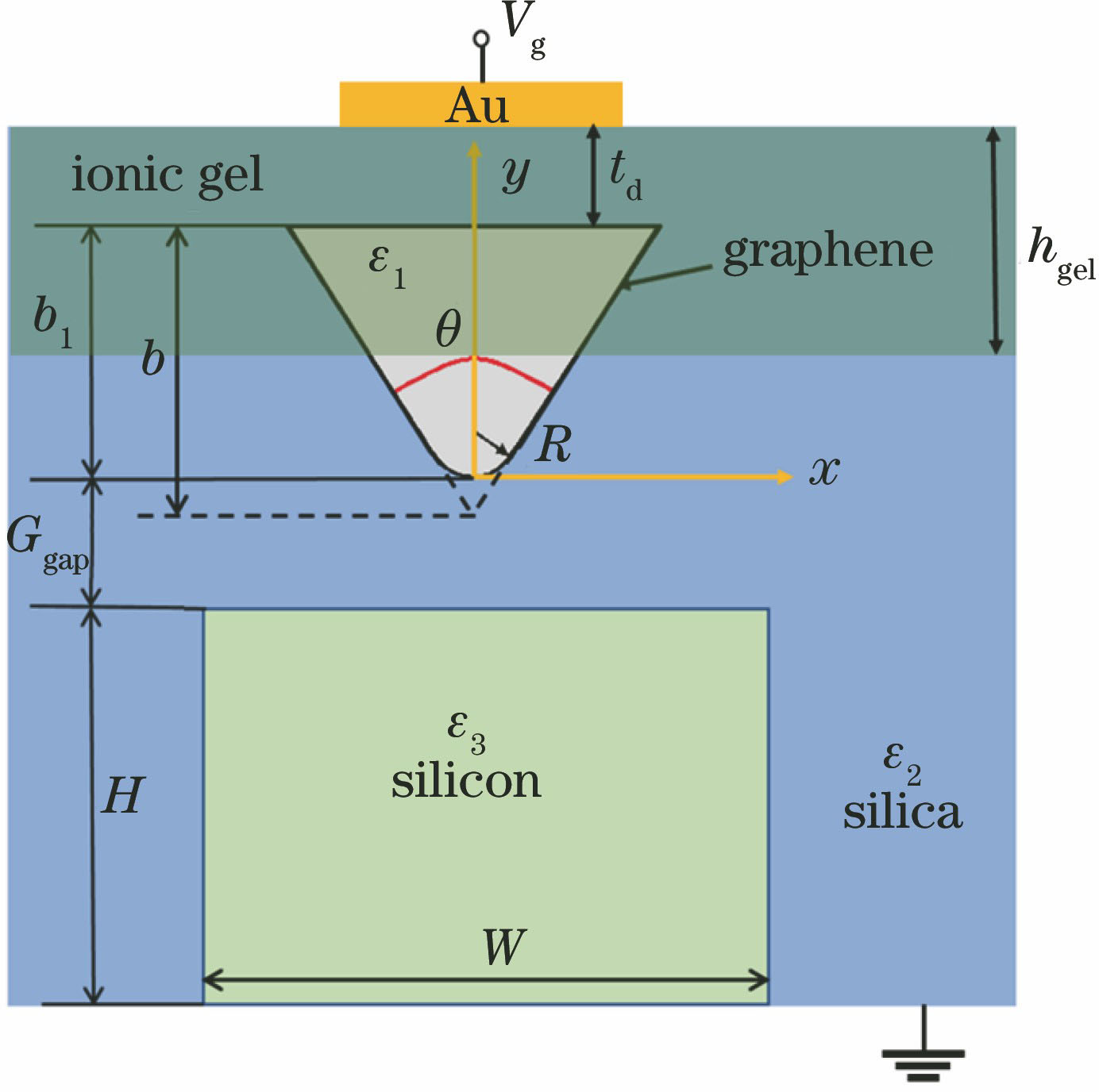
Fig. 1. Structural diagram of waveguide
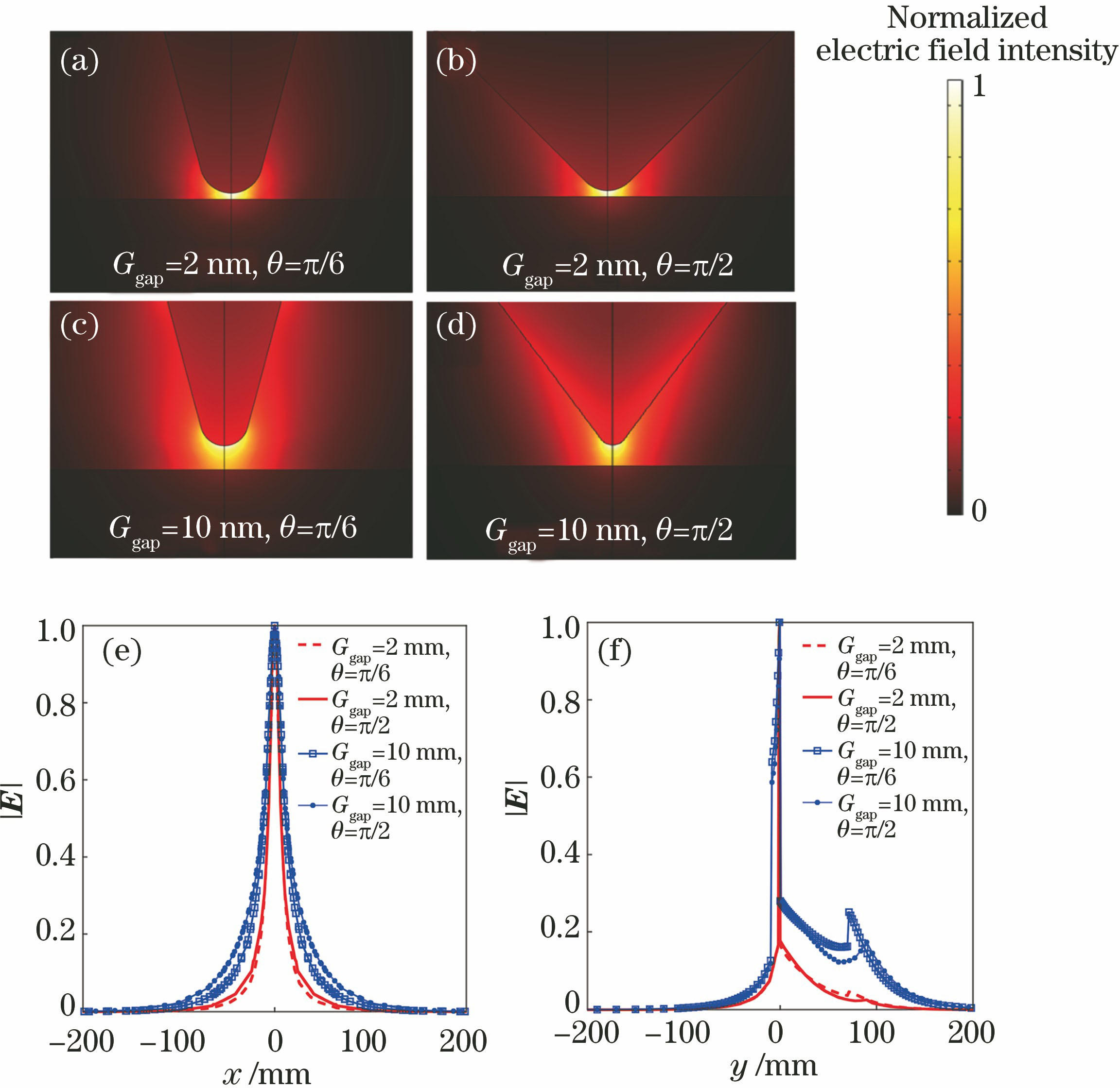
Fig. 2. Normalized electric field intensity distributions of fundamental mode when μc=0.5 eV,f0=30 THz,and R=10 nm. (a) Under θ=π/6, Ggap=2 nm; (b) under θ=π/2, Ggap=2 nm;(c) under θ =π/6, Ggap=10 nm; (d) under θ=π/2, Ggap=10 nm; normalized electric field intensity distributions along (e) x and (f) y directions
Fig. 3. Modal properties versus gap when μc=0.5 eV,f0=30 THz, R=10 nm, and θ=π/2. (a) Re(neff); (b) propagation length; (c) normalized mode area
Fig. 4. Modal properties versus θ when μc=0.5 eV,f0=30 THz, Ggap=2 nm, and R=10 nm. (a) Re(neff); (b) propagation length; (c) normalized mode area
Fig. 5. Modal properties with respect to R when μc=0.5 eV,f0=30 THz,Ggap=2 nm,and θ=π/3. (a) Re(neff), (b) propagation length; (c) normalized mode area
Fig. 6. Modal properties versus frequency under different chemical potential values when Ggap=2 nm, θ=π/3,and R=10 nm. (a) Re(neff); (b) propagation length; (c) normalized mode area

Set citation alerts for the article
Please enter your email address
© Copyright 2018-2021 | Chinese Laser Press. All Rights Reserved 沪ICP备15018463号-20