• Advanced Photonics
  • Vol. 5, Issue 2, 024001 (2023)
Jin Yao1、†, Rong Lin1, Mu Ku Chen1、2、3, and Din Ping Tsai1、2、3、*
Author Affiliations
  • 1City University of Hong Kong, Department of Electrical Engineering, Hong Kong, China
  • 2City University of Hong Kong, Centre for Biosystems, Neuroscience, and Nanotechnology, Hong Kong, China
  • 3City University of Hong Kong, State Key Laboratory of Terahertz and Millimeter Waves, Hong Kong, China
  • show less
    DOI: 10.1117/1.AP.5.2.024001 Cite this Article Set citation alerts
    Jin Yao, Rong Lin, Mu Ku Chen, Din Ping Tsai. Integrated-resonant metadevices: a review[J]. Advanced Photonics, 2023, 5(2): 024001 Copy Citation Text show less
    Schematic diagram of organization in this review.
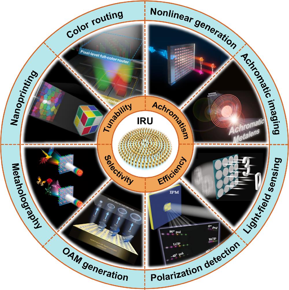
    Fig. 1. Schematic diagram of organization in this review.
    (a) Phase profile for a broadband achromatic metalens. (b) Schematic diagrams and phase spectra of three types of IRUs with phase compensations of Δφ1(λ), Δφ2(λ), and Δφ3(λ), respectively.
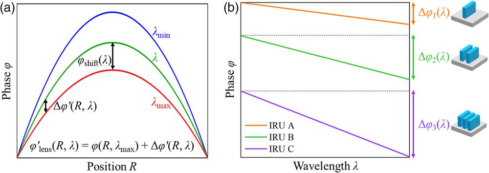
    Fig. 2. (a) Phase profile for a broadband achromatic metalens. (b) Schematic diagrams and phase spectra of three types of IRUs with phase compensations of Δφ1(λ), Δφ2(λ), and Δφ3(λ), respectively.
    Achromatic integrated-resonant metadevices: IRUs and intensity distributions at different wavelengths. (a) Coupled rectangular silicon resonators, three discrete wavelengths of 1300, 1550, and 1800 nm.43" target="_self" style="display: inline;">43 (b) TiO2 nanopillars tiled on a SiO2 spacer layer above an Al-coated fused silica substrate, narrowband from 490 to 550 nm.44" target="_self" style="display: inline;">44 (c) Au nanorods, broadband from 1200 to 1680 nm.33" target="_self" style="display: inline;">33 (d) GaN nanopillars and nanoholes, broadband from 400 to 660 nm.45" target="_self" style="display: inline;">45 (e) TiO2 nanofins, broadband from 470 to 670 nm.46" target="_self" style="display: inline;">46 (f) Silicon nanopillars, broadband from 1200 to 1650 nm.47" target="_self" style="display: inline;">47
    Fig. 3. Achromatic integrated-resonant metadevices: IRUs and intensity distributions at different wavelengths. (a) Coupled rectangular silicon resonators, three discrete wavelengths of 1300, 1550, and 1800 nm.43 (b) TiO2 nanopillars tiled on a SiO2 spacer layer above an Al-coated fused silica substrate, narrowband from 490 to 550 nm.44 (c) Au nanorods, broadband from 1200 to 1680 nm.33 (d) GaN nanopillars and nanoholes, broadband from 400 to 660 nm.45 (e) TiO2 nanofins, broadband from 470 to 670 nm.46 (f) Silicon nanopillars, broadband from 1200 to 1650 nm.47
    Efficiency-enhanced integrated-resonant metadevices: schematic diagrams, scanning electron microscope (SEM) images, and spectral responses. (a) Al multinanorods to enhance broadband polarization conversion efficiency.38" target="_self" style="display: inline;">38 (b) Four VSRRs for isotropic perfect absorption.54" target="_self" style="display: inline;">54 (c) 3D Au/Si3N4 Archimedean spirals to enhance the optical chirality.55" target="_self" style="display: inline;">55 (d) Coupled Au pillars and gratings used for a high Q factor under highly focused incidence.56" target="_self" style="display: inline;">56 (e) Silicon nanodisks with Kerker condition to achieve high transmission accompanied by full 2π phase coverage.57" target="_self" style="display: inline;">57 (f) VSRRs covered with a perforated Au film to excite the anapole mode.58" target="_self" style="display: inline;">58 (g) Silicon rectangular bar resonators combined with ring resonators to generate the Fano resonance.59" target="_self" style="display: inline;">59 (h) AlGaAs nanodisk with mode coupling to form quasi-BIC.60" target="_self" style="display: inline;">60
    Fig. 4. Efficiency-enhanced integrated-resonant metadevices: schematic diagrams, scanning electron microscope (SEM) images, and spectral responses. (a) Al multinanorods to enhance broadband polarization conversion efficiency.38 (b) Four VSRRs for isotropic perfect absorption.54 (c) 3D Au/Si3N4 Archimedean spirals to enhance the optical chirality.55 (d) Coupled Au pillars and gratings used for a high Q factor under highly focused incidence.56 (e) Silicon nanodisks with Kerker condition to achieve high transmission accompanied by full 2π phase coverage.57 (f) VSRRs covered with a perforated Au film to excite the anapole mode.58 (g) Silicon rectangular bar resonators combined with ring resonators to generate the Fano resonance.59 (h) AlGaAs nanodisk with mode coupling to form quasi-BIC.60
    Property-selective integrated-resonant metadevices. (a) Two sets of silicon nanoholes with q-BIC to realize wavefront shaping at selected wavelengths: schematic diagram, SEM image, and xy and xz plane intensity distributions at different wavelengths.69" target="_self" style="display: inline;">69 (b) GaN nanopillars for OAM selectivity in metasurface holography: schematic diagram and experimental metaholograms with four OAM topological charges.71" target="_self" style="display: inline;">71 (c) Diatomic Au VSRRs allow polarization-selective perfect absorption: schematic diagram, reflection spectra with different polarization states, and SEM images.73" target="_self" style="display: inline;">73 (d) U-shaped amorphous silicon nanopillars for angle-selective metahologram: schematic diagram and measured reflected images at normal and 30 deg illumination angles.75" target="_self" style="display: inline;">75 (e) Notched silicon bars to achieve metalens with intensity selectivity: schematic diagram and field intensity profiles with different input intensities.76" target="_self" style="display: inline;">76
    Fig. 5. Property-selective integrated-resonant metadevices. (a) Two sets of silicon nanoholes with q-BIC to realize wavefront shaping at selected wavelengths: schematic diagram, SEM image, and xy and xz plane intensity distributions at different wavelengths.69 (b) GaN nanopillars for OAM selectivity in metasurface holography: schematic diagram and experimental metaholograms with four OAM topological charges.71 (c) Diatomic Au VSRRs allow polarization-selective perfect absorption: schematic diagram, reflection spectra with different polarization states, and SEM images.73 (d) U-shaped amorphous silicon nanopillars for angle-selective metahologram: schematic diagram and measured reflected images at normal and 30 deg illumination angles.75 (e) Notched silicon bars to achieve metalens with intensity selectivity: schematic diagram and field intensity profiles with different input intensities.76
    Tunable integrated-resonant metadevices. (a) TiO2 nanoposts with polarization-dependent response for varifocal metalens: schematic diagram and intensity distributions with horizontally and vertically polarized incidence.79" target="_self" style="display: inline;">79 (b) Coupled anisotropic silicon nanofins with thermo-optic effects to obtain thermally reconfigurable metalens: schematic diagram and intensity profiles for different temperatures.81" target="_self" style="display: inline;">81 (c) Eight integrated CMOS switches allow digitally programmable wavefront shaping based on electric stimuli: schematic diagram, far-field intensity distributions, and fabricated metasurface chip.84" target="_self" style="display: inline;">84 (d) Coupled Au nanobars for environment-based dynamic metahologram: schematic diagram and hologram images with different environments.85" target="_self" style="display: inline;">85 (e) Interleaved Al and phase change material GST stacked nanorods utilized for all-optical cryptography: schematic diagram and hologram images for three states of GST.89" target="_self" style="display: inline;">89 (f) Au nanorods integrated on stretched PDMS to acquire the zoom lens: schematic diagram and beam profiles with distinct stretch ratios.90" target="_self" style="display: inline;">90
    Fig. 6. Tunable integrated-resonant metadevices. (a) TiO2 nanoposts with polarization-dependent response for varifocal metalens: schematic diagram and intensity distributions with horizontally and vertically polarized incidence.79 (b) Coupled anisotropic silicon nanofins with thermo-optic effects to obtain thermally reconfigurable metalens: schematic diagram and intensity profiles for different temperatures.81 (c) Eight integrated CMOS switches allow digitally programmable wavefront shaping based on electric stimuli: schematic diagram, far-field intensity distributions, and fabricated metasurface chip.84 (d) Coupled Au nanobars for environment-based dynamic metahologram: schematic diagram and hologram images with different environments.85 (e) Interleaved Al and phase change material GST stacked nanorods utilized for all-optical cryptography: schematic diagram and hologram images for three states of GST.89 (f) Au nanorods integrated on stretched PDMS to acquire the zoom lens: schematic diagram and beam profiles with distinct stretch ratios.90
    Integrated-resonant metadevices for achromatic imaging. (a) Reflective achromatic metalens made of Au IRUs: (left) SEM image, (middle) optical image of the metalens, and (right) intensity profiles at different incident wavelengths.33" target="_self" style="display: inline;">33 (b) Transmissive achromatic metalens made of TiO2 IRUs in the visible: (left) image of USAF target and (right) image of Siemens star pattern.46" target="_self" style="display: inline;">46 (c) Transmissive achromatic metalens made of GaN IRUs in the visible: (left) SEM image, (middle) image of USAF target, and (right) full-color image of Alcedinidae.45" target="_self" style="display: inline;">45 (d) Achromatic polarization-insensitive metalens made of TiO2 IRUs in the visible: (left) SEM image and (right) image of USAF target corresponding to number 6.52" target="_self" style="display: inline;">52 (e) Achromatic polarization-insensitive metalens made of TiO2 IRUs in the NIR spectrum: (left) SEM image, (right) results of upconversion fluorescent imaging (top row: NCs and polystyrene spheres and bottom row: HeLa cells).53" target="_self" style="display: inline;">53 (f) Achromatic metalens made of TiO2 IRUs using a neural network: (left) SEM image and (right) three letters images with different linewidths.96" target="_self" style="display: inline;">96
    Fig. 7. Integrated-resonant metadevices for achromatic imaging. (a) Reflective achromatic metalens made of Au IRUs: (left) SEM image, (middle) optical image of the metalens, and (right) intensity profiles at different incident wavelengths.33 (b) Transmissive achromatic metalens made of TiO2 IRUs in the visible: (left) image of USAF target and (right) image of Siemens star pattern.46 (c) Transmissive achromatic metalens made of GaN IRUs in the visible: (left) SEM image, (middle) image of USAF target, and (right) full-color image of Alcedinidae.45 (d) Achromatic polarization-insensitive metalens made of TiO2 IRUs in the visible: (left) SEM image and (right) image of USAF target corresponding to number 6.52 (e) Achromatic polarization-insensitive metalens made of TiO2 IRUs in the NIR spectrum: (left) SEM image, (right) results of upconversion fluorescent imaging (top row: NCs and polystyrene spheres and bottom row: HeLa cells).53 (f) Achromatic metalens made of TiO2 IRUs using a neural network: (left) SEM image and (right) three letters images with different linewidths.96
    Integrated-resonant metadevices for light-field sensing. (a) Imaging and reconstruction process of a depth sensor composed of TiO2 IRUs.97" target="_self" style="display: inline;">97 (b) (Left) Schematic diagram of integral imaging using a SiN IRUs-based achromatic metalenses array and (right) reconstructed images at different locations with various incident wavelengths.98" target="_self" style="display: inline;">98 (c) (Left) Schematic of light-field sensing using an achromatic metalenses array consisting of GaN IRUs and (right) reconstruction images, and depth maps with different depths.99" target="_self" style="display: inline;">99 (d) (Left) Schematic of edge detection relying on a GaN IRUs-based achromatic metalenses array and (right) experiment results: light-field raw data, partial raw data, 1D edge image result, 3D edge images with different depths.100" target="_self" style="display: inline;">100 (e) (Left) Schematic of 3D image system realized by TiO2 IRUs and neural network and (right) reconstruction results of full-color images and depth maps.101" target="_self" style="display: inline;">101 (f) Schematic of a depth-sensing system composed of GaN IRUs in all-light-level.102" target="_self" style="display: inline;">102
    Fig. 8. Integrated-resonant metadevices for light-field sensing. (a) Imaging and reconstruction process of a depth sensor composed of TiO2 IRUs.97 (b) (Left) Schematic diagram of integral imaging using a SiN IRUs-based achromatic metalenses array and (right) reconstructed images at different locations with various incident wavelengths.98 (c) (Left) Schematic of light-field sensing using an achromatic metalenses array consisting of GaN IRUs and (right) reconstruction images, and depth maps with different depths.99 (d) (Left) Schematic of edge detection relying on a GaN IRUs-based achromatic metalenses array and (right) experiment results: light-field raw data, partial raw data, 1D edge image result, 3D edge images with different depths.100 (e) (Left) Schematic of 3D image system realized by TiO2 IRUs and neural network and (right) reconstruction results of full-color images and depth maps.101 (f) Schematic of a depth-sensing system composed of GaN IRUs in all-light-level.102
    Integrated-resonant metadevices for polarization detection. (a) Schematic of Au IRUs-based spectropolarimetry.107" target="_self" style="display: inline;">107 (b) Schematic of Al IRU-based versatile polarization detector under linearly polarized incident light.108" target="_self" style="display: inline;">108 (c) (Left) Schematic of Al IRU-based visible polarimetry under incident light with unknown polarization state and (right) measurement results after the y-polarized light passes through a single layer of BOPP film.109" target="_self" style="display: inline;">109 (d) Meta-Hartmann–Shack array based on silicon IRUs: (top) intensity distributions, (middle) images with meta-Hartmann–Shack array, and (bottom) polarization profiles of focal spots for radially polarized incident beam and azimuthally polarized beam.110" target="_self" style="display: inline;">110 (e) Schematic diagram and experimental results of silicon IRU-based polarization imaging system.111" target="_self" style="display: inline;">111 (f) Alpha-silicon IRU-based metasurfaces for polarization detection and manipulation: (top) versatile polarization generator, schematic diagram, and intensity profiles with different polarization states and (bottom) vectorial holographic display.112" target="_self" style="display: inline;">112
    Fig. 9. Integrated-resonant metadevices for polarization detection. (a) Schematic of Au IRUs-based spectropolarimetry.107 (b) Schematic of Al IRU-based versatile polarization detector under linearly polarized incident light.108 (c) (Left) Schematic of Al IRU-based visible polarimetry under incident light with unknown polarization state and (right) measurement results after the y-polarized light passes through a single layer of BOPP film.109 (d) Meta-Hartmann–Shack array based on silicon IRUs: (top) intensity distributions, (middle) images with meta-Hartmann–Shack array, and (bottom) polarization profiles of focal spots for radially polarized incident beam and azimuthally polarized beam.110 (e) Schematic diagram and experimental results of silicon IRU-based polarization imaging system.111 (f) Alpha-silicon IRU-based metasurfaces for polarization detection and manipulation: (top) versatile polarization generator, schematic diagram, and intensity profiles with different polarization states and (bottom) vectorial holographic display.112
    Integrated-resonant metadevices for OAM generation. (a) (Top) Schematic and SEM image of spin-controlled Au IRUs-based OAM generator with multimodes and (bottom) three-by-two spin-dependent OAM wavefronts with the desired topological charges.127" target="_self" style="display: inline;">127 (b) (Upper left) Schematic of tunable OAM generator based on GST IRUs, (upper right) interference patterns, and (bottom) diffraction profiles at different crystallization levels.128" target="_self" style="display: inline;">128 (c) (Top) Modulation of IRU by hydrogenation and dehydrogenation, (middle) OAM switching, and (bottom) schematic of hologram switching.129" target="_self" style="display: inline;">129 (d) Intensity and phase profiles with different polarization states of silicon IRU-based metadevice.130" target="_self" style="display: inline;">130 (e) OAM generator made of multilayer IRUs: (left) structure diagram and (right) schematic principle of the OAM generator with integer and fractional modes engineered by polarization modulation.131" target="_self" style="display: inline;">131
    Fig. 10. Integrated-resonant metadevices for OAM generation. (a) (Top) Schematic and SEM image of spin-controlled Au IRUs-based OAM generator with multimodes and (bottom) three-by-two spin-dependent OAM wavefronts with the desired topological charges.127 (b) (Upper left) Schematic of tunable OAM generator based on GST IRUs, (upper right) interference patterns, and (bottom) diffraction profiles at different crystallization levels.128 (c) (Top) Modulation of IRU by hydrogenation and dehydrogenation, (middle) OAM switching, and (bottom) schematic of hologram switching.129 (d) Intensity and phase profiles with different polarization states of silicon IRU-based metadevice.130 (e) OAM generator made of multilayer IRUs: (left) structure diagram and (right) schematic principle of the OAM generator with integer and fractional modes engineered by polarization modulation.131
    Integrated-resonant metadevices for metaholography. (a) Metahologram images can be switched by the states of linearly polarized light based on Au IRUs: (left) schematic of the metahologram and (right) reconstructed images.155" target="_self" style="display: inline;">155 (b) Hologram patterns of an Au IRU-based metadevice dependent on incident polarization states and wavelengths.156" target="_self" style="display: inline;">156 (c) Vectorial metahologram based on Ag IRUs: (upper left) predesigned pattern, (bottom left) SEM image, and (right) measured results of holographic images.157" target="_self" style="display: inline;">157 (d) Schematic of the polarization-sensitive multicolor metahologram composed of Al IRUs.158" target="_self" style="display: inline;">158 (e) (Left) Schematic of the 3D full-color metahologram based on silicon IRUs and (right) 3D full-color reconstructed results under RCP incident light.159" target="_self" style="display: inline;">159 (f) Reconstructed results of full-color complex-amplitude vectorial hologram based on Al IRUs, illuminating by (left) laser beam with different colors and (right) white light.160" target="_self" style="display: inline;">160
    Fig. 11. Integrated-resonant metadevices for metaholography. (a) Metahologram images can be switched by the states of linearly polarized light based on Au IRUs: (left) schematic of the metahologram and (right) reconstructed images.155 (b) Hologram patterns of an Au IRU-based metadevice dependent on incident polarization states and wavelengths.156 (c) Vectorial metahologram based on Ag IRUs: (upper left) predesigned pattern, (bottom left) SEM image, and (right) measured results of holographic images.157 (d) Schematic of the polarization-sensitive multicolor metahologram composed of Al IRUs.158 (e) (Left) Schematic of the 3D full-color metahologram based on silicon IRUs and (right) 3D full-color reconstructed results under RCP incident light.159 (f) Reconstructed results of full-color complex-amplitude vectorial hologram based on Al IRUs, illuminating by (left) laser beam with different colors and (right) white light.160
    Integrated-resonant metadevices for nanoprinting. (a) Polarization-sensitive nanoprinting using TiO2 IRUs: (left) schematic of setup and (right) measured meta-nanoprinting patterns under LCP/RCP illumination.165" target="_self" style="display: inline;">165 (b) Angle-multiplexing nanoprinting with hologram using Ag IRUs: (left) sketch of the metadevice and (right) experiment results of nanoprinting and holographic patterns.162" target="_self" style="display: inline;">162 (c) Integrating color printing with holography based on silicon IRUs: (left) schematic of principle and (right) measured patterns of nanoprinting and hologram.166" target="_self" style="display: inline;">166 (d) Full-color nanoprint-hologram synchronous realization using c-silicon IRUs: (left) schematic of principle and (right) measured hologram patterns under various incident lights.167" target="_self" style="display: inline;">167 (e) (Top) Arrangement and principle of c-silicon IRUs and (bottom) schematic of displaying images in three channels.168" target="_self" style="display: inline;">168 (f) Illustration of vectorial holographic color prints with the assistance of IRU and liquid crystal.169" target="_self" style="display: inline;">169
    Fig. 12. Integrated-resonant metadevices for nanoprinting. (a) Polarization-sensitive nanoprinting using TiO2 IRUs: (left) schematic of setup and (right) measured meta-nanoprinting patterns under LCP/RCP illumination.165 (b) Angle-multiplexing nanoprinting with hologram using Ag IRUs: (left) sketch of the metadevice and (right) experiment results of nanoprinting and holographic patterns.162 (c) Integrating color printing with holography based on silicon IRUs: (left) schematic of principle and (right) measured patterns of nanoprinting and hologram.166 (d) Full-color nanoprint-hologram synchronous realization using c-silicon IRUs: (left) schematic of principle and (right) measured hologram patterns under various incident lights.167 (e) (Top) Arrangement and principle of c-silicon IRUs and (bottom) schematic of displaying images in three channels.168 (f) Illustration of vectorial holographic color prints with the assistance of IRU and liquid crystal.169
    Integrated-resonant metadevices for color routing. (a) Dual-band color router with dolmen IRUs: (left) schematic of the device and (right) measured Fourier image.170" target="_self" style="display: inline;">170 (b) Tri-band color router with doublet IRUs for the wavelengths of 1180, 1400, and 1680 nm: (left) schematic of the tri-band color router and (right) measured intensity distributions and focal spot profiles.171" target="_self" style="display: inline;">171 (c) Tri-band color router with nanobeams IRUs in the visible: (left) schematic of setup and (right) image generated by the color router.172" target="_self" style="display: inline;">172 (d) Sensitivity and noise tolerance performance of tri-band color router with nanoposts IRUs: (left) comparison of the total amount of light in each configuration and (right) color images reconstructed by each configuration with different sensor noise.173" target="_self" style="display: inline;">173 (e) Full-color router displayed a Bayer pattern using nanopillars IRUs: (left) principle of full-color routing and (right) measured results at the focal plane under different wavelengths.174" target="_self" style="display: inline;">174 (f) Nanoposts IRUs color-sorting device: (left) focal intensity profile and (right) comparison results of color objects imaged by two sensors.175" target="_self" style="display: inline;">175
    Fig. 13. Integrated-resonant metadevices for color routing. (a) Dual-band color router with dolmen IRUs: (left) schematic of the device and (right) measured Fourier image.170 (b) Tri-band color router with doublet IRUs for the wavelengths of 1180, 1400, and 1680 nm: (left) schematic of the tri-band color router and (right) measured intensity distributions and focal spot profiles.171 (c) Tri-band color router with nanobeams IRUs in the visible: (left) schematic of setup and (right) image generated by the color router.172 (d) Sensitivity and noise tolerance performance of tri-band color router with nanoposts IRUs: (left) comparison of the total amount of light in each configuration and (right) color images reconstructed by each configuration with different sensor noise.173 (e) Full-color router displayed a Bayer pattern using nanopillars IRUs: (left) principle of full-color routing and (right) measured results at the focal plane under different wavelengths.174 (f) Nanoposts IRUs color-sorting device: (left) focal intensity profile and (right) comparison results of color objects imaged by two sensors.175
    Integrated-resonant metadevices for nonlinear effect. (a) THG with high efficiency based on metal–dielectric IRUs: (left) schematic of the configuration, (middle) SEM image and normalized electric field distribution, and (right) THG spectra.182" target="_self" style="display: inline;">182 (b) THG boosted by all-dielectric IRUs: (left) TH spectra under different incident conditions of polarization states and (right) TH spectra of an unpatterned silicon film.183" target="_self" style="display: inline;">183 (c) Reshaping TH spectra using all-dielectric IRUs: (left) schematic diagram and (right) tuning the TH spectral response under different distances between the nanodisks.184" target="_self" style="display: inline;">184 (d) Improving the efficiency of SH power collection using AlGaAs IRUs: (left) SEM images of a disk and the IRU and their corresponding SH emission patterns and (right) fraction of SH emitted at different NAs compared to the total collected SH.185" target="_self" style="display: inline;">185 (e) Nonlinear imaging by Au IRUs: (left) SEM image of the metadevice for nonlinear hologram and (right) measured hologram image.186" target="_self" style="display: inline;">186 (f) Complex quantum states generated by GaAs IRUs: (left) schematic of generating complex quantum states and (right) SPDC spectrum to illustrate the entangled process.187" target="_self" style="display: inline;">187
    Fig. 14. Integrated-resonant metadevices for nonlinear effect. (a) THG with high efficiency based on metal–dielectric IRUs: (left) schematic of the configuration, (middle) SEM image and normalized electric field distribution, and (right) THG spectra.182 (b) THG boosted by all-dielectric IRUs: (left) TH spectra under different incident conditions of polarization states and (right) TH spectra of an unpatterned silicon film.183 (c) Reshaping TH spectra using all-dielectric IRUs: (left) schematic diagram and (right) tuning the TH spectral response under different distances between the nanodisks.184 (d) Improving the efficiency of SH power collection using AlGaAs IRUs: (left) SEM images of a disk and the IRU and their corresponding SH emission patterns and (right) fraction of SH emitted at different NAs compared to the total collected SH.185 (e) Nonlinear imaging by Au IRUs: (left) SEM image of the metadevice for nonlinear hologram and (right) measured hologram image.186 (f) Complex quantum states generated by GaAs IRUs: (left) schematic of generating complex quantum states and (right) SPDC spectrum to illustrate the entangled process.187
    IRUWavelengthEfficiency (%)NADiameterPolarizationRef.
    TiO2 nanopillars490 to 550 nm150.2200  μmCircular44
    Coupled Al nanorods420 to 650 nm200.12441.86  μmCircular38
    Coupled Au nanorods1200 to 1680 nm12.440.26855.55  μmCircular33
    GaN nanopillars and nanoholes400 to 660 nm400.10625  μmCircular45
    Coupled TiO2 nanofins470 to 670 nm200.225  μmCircular46
    Coupled TiO2 nanofins470 to 700 nm350.0751.5 mmCircular50
    Silicon nanopillars and nanoholes375 to 1000 μm680.38510 mmCircular51
    Silicon nanopillars1200 to 1650 nm320.13200  μmInsensitive47
    Coupled TiO2 nanofins460 to 700 nm350.226.4  μmInsensitive52
    TiO2 nanopillars650 to 1000 nm88.50.125  μmInsensitive53
    Table 1. Performances of broadband achromatic metalenses.
    Jin Yao, Rong Lin, Mu Ku Chen, Din Ping Tsai. Integrated-resonant metadevices: a review[J]. Advanced Photonics, 2023, 5(2): 024001
    Download Citation