• Advanced Photonics
  • Vol. 5, Issue 2, 024001 (2023)
Jin Yao1、†, Rong Lin1, Mu Ku Chen1、2、3, and Din Ping Tsai1、2、3、*
Author Affiliations
  • 1City University of Hong Kong, Department of Electrical Engineering, Hong Kong, China
  • 2City University of Hong Kong, Centre for Biosystems, Neuroscience, and Nanotechnology, Hong Kong, China
  • 3City University of Hong Kong, State Key Laboratory of Terahertz and Millimeter Waves, Hong Kong, China
  • show less
    DOI: 10.1117/1.AP.5.2.024001 Cite this Article Set citation alerts
    Jin Yao, Rong Lin, Mu Ku Chen, Din Ping Tsai. Integrated-resonant metadevices: a review[J]. Advanced Photonics, 2023, 5(2): 024001 Copy Citation Text show less

    Abstract

    Integrated-resonant units (IRUs), associating various meta-atoms, resonant modes, and functionalities into one supercell, have been promising candidates for tailoring composite and multifunctional electromagnetic responses with additional degrees of freedom. Integrated-resonant metadevices can overcome many bottlenecks in conventional optical devices, such as broadband achromatism, efficiency enhancement, response selectivity, and continuous tunability, offering great potential for performant and versatile application scenarios. We focus on the recent progress of integrated-resonant metadevices. Starting from the design principle of IRUs, a variety of IRU-based characteristics and subsequent practical applications, including achromatic imaging, light-field sensing, polarization detection, orbital angular momentum generation, metaholography, nanoprinting, color routing, and nonlinear generation, are introduced. Existing challenges in this field and opinions on future research directions are also provided.

    1 Introduction

    Metasurfaces comprising artificial photonic nanostructures (meta-atoms) have aroused tremendous attention due to their profound potential in flat optics. They possess the capability of flexibly manipulating electromagnetic responses, such as amplitude, phase, polarization state, and spectral response in an efficient and compact way.15 Various devices and applications have been developed based on metaoptics, for example, beam shaping,69 bioimaging,1012 metaholography,1315 lasing,16,17 sensing,18,19 optical nonlinearity,2025 and quantum sources.2629 However, conventional metadevices mainly comprise a single type of meta-atom. Their fundamental designs lack degrees of freedom, leading to the limited controllability of optical responses. Suffering from unifunctional and low-dimensional properties in general, it is difficult for them to realize the complex functionalities, such as continuous chromatic aberration correction, multiplexing, multiband electromagnetic control, restricting their performance, and versatile applications.30,31

    Integrated-resonant units (IRUs), integrating multiple meta-atoms, resonant modes, and functionalities into one supercell, can realize desired responses and functionalities exceeding conventional meta-atoms.32 The concept of the IRU was first proposed and utilized in achromatic metalenses requiring various phase compensations.33 Compared with the concept of the supercell, the IRU is relatively a more specific area that focuses more on the integration and interaction of different resonant responses. Since each meta-atom and resonant mode can be individually designed, IRUs provide additional design freedoms, such as the number, geometric parameters, constituent materials, and properties of each meta-atom and resonance. The meta-atoms can be integrated both in parallell and vertical directions into the IRUs with different light–matter interaction mechanisms.34 The coupling and interferences between meta-atoms and resonances are also significant in IRUs. They can be both useful and detrimental depending on the desired functionality, which requires careful design based on their near-field coupling strengths.35 By arranging these versatile IRUs into the metadevice, integrated-resonant metadevices have shown preeminent performance and versatilities outperforming their conventional counterparts.36,37

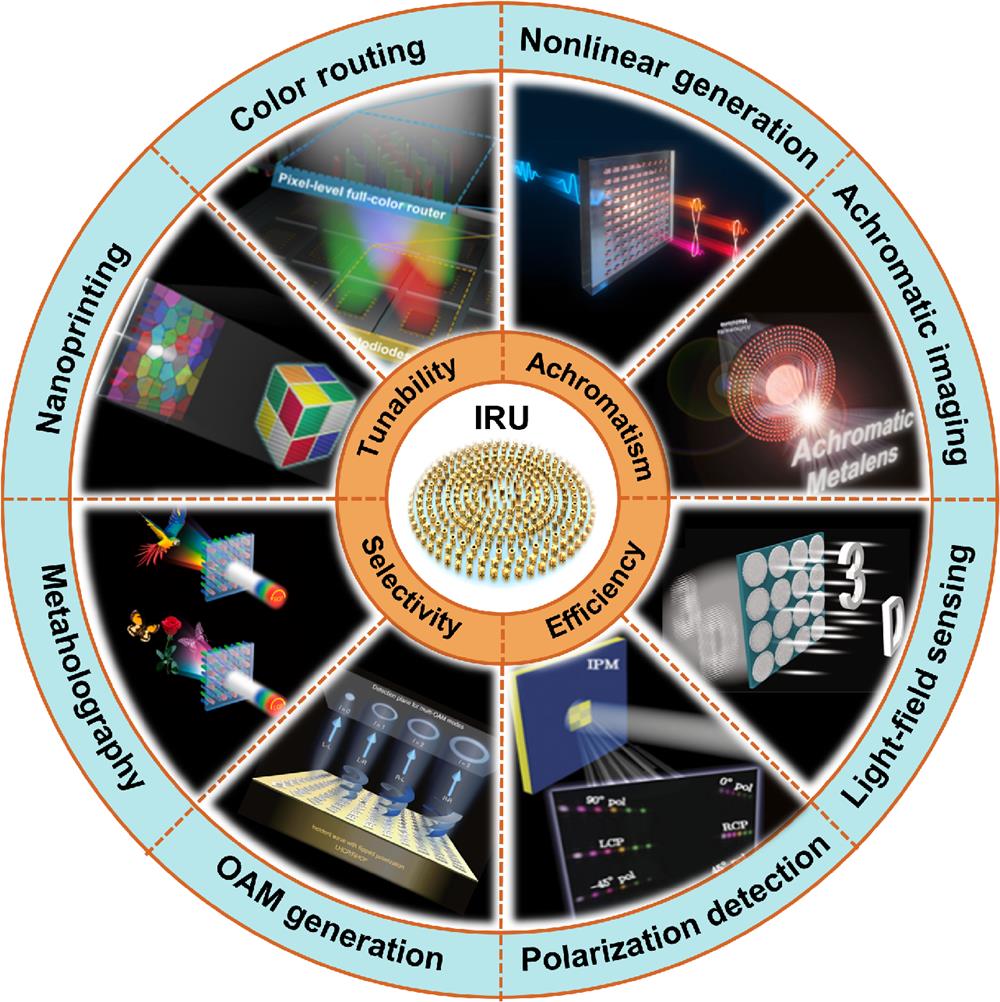
    This review focuses on the recent progress in the development of integrated-resonant metadevices. The organization has three main parts, which are shown in Fig. 1. First, the design principle and working mechanism of the IRU are introduced. A metalens with IRUs correcting the chromatic aberration is discussed in detail. Then IRUs with different optimized functionalities, including achromatism, efficiency, selectivity, and tunability, are presented. These characteristics produce versatile applications in achromatic imaging, light-field sensing, polarization detection, orbital angular momentum (OAM) generation, metaholography, nanoprinting, color routing, and nonlinear generation, etc., which are reviewed as well. This review concludes with existing challenges and future prospects in this field.

    Schematic diagram of organization in this review.

    Figure 1.Schematic diagram of organization in this review.

    2 Principle

    To realize the multiple functionalities of the metadevice, each meta-atom requires the optimization of constituent materials, geometric parameters, resonant modes, and so on. The integrated-resonant metadevice layout is acquired based on engineering the interaction among meta-atoms and arranging each IRU according to demanded responses. In the design process, many electromagnetic responses can be taken into consideration, such as amplitude (E), phase (φ), polarization (p), effective nonlinear coefficient (χ), working wavelength range (λ), and local position (x,y). This process can be conceptually described as a system of equations,38metadevice(t,λ,I,φ,p,σ,l,nonlinear,quantum)=IRUs{E(x,y,t,λ)φ(x,y,t,λ)p(x,y,t,λ)χ(x,y,t,λ),where tenability (t), working wavelength range (λ), efficiency (I), phase distribution (φ), polarization state (p), spin angular momentum (SAM) (σ), OAM (l), nonlinear or quantum effect, etc., are desired optical properties in the integrated-resonant metadevice. In practical operations, it is difficult to optimize all electromagnetic responses in a metadevice, and some of them are even competing, so a trade-off among different performance parameters has to be made. Unimportant characteristics can be sacrificed to preserve the desired features.

    Based on the coupling strength between meta-atoms and resonant modes, there are two main methods to design IRUs. If the interaction is weak and insignificant, each meta-atom and resonance can be independently controlled with different properties, such as phase, amplitude, wavelength, and polarization. The IRUs can work at multiple channels without the consideration of undesired cross talk. This type of IRU is more suitable for multiband operation, multiplexing, and multifunctionality. The other design method is based on the near-field coupling between meta-atoms and resonances. Meta-atoms with near-field coupling can be described as coupled dipoles exhibiting hybridization. According to the relative direction of the two dipoles, symmetric and antisymmetric modes are created.39 The antisymmetric mode with low radiative losses and high-resonant quality factors (Q factors) can be obtained by involving a slight asymmetry, such as geometry and incidence. IRUs with strong coupling are beneficial in achieving high efficiency, special selectivity, and other complex functionalities.

    To elaborate on the design principle of the IRU, the broadband achromatic metalens is discussed here as an example. The phase profile of a metalens can be described as40φ(R,λ)=2π(R2+f2f)1λ,where R is the radial coordinate, λ is the working wavelength, and f is the designed focal length. According to this equation, a metalens can only work efficiently at a single wavelength, whereas the focal lengths at other wavelengths will deviate from the designed one, producing chromatic aberration and limiting the performance of the metalens. To solve this problem, Tsai et al.33 developed the strategy of IRU and a differential phase (DP) equation by introducing additional phase compensation. For the achromatic metalens with working wavelength λ{λmin,λmax}, where λmin and λmax are the boundaries of the target wavelength range, Eq. (2) can be expressed as a DP equation, φlens(R,λ)=φ(R,λmax)+Δφ(R,λ),where Δφ(R,λ)=2π(R2+f2f)(1λ1λmax).

    The basic phase φ(R,λmax) is independent of the working wavelength λ, which can be realized by the geometric phase based on the rotation of meta-atoms.41 The phase difference Δφ(R,λ) has an inversely proportional relationship with λ, so each IRU needs to be engineered to simultaneously possess a linear phase dispersion and provide the desired Δφ(R,λ). These two parts of the phase can be directly combined without interfering with each other.

    To further enhance the phase compensation effect, an additional phase shift is involved without detriment to the focusing capability of the metalens, as shown in Fig. 2(a). The phase profile of the achromatic metalens can be adjusted to φlens(R,λ)=2π(R2+f2f)1λ+φshift(λ).

    (a) Phase profile for a broadband achromatic metalens. (b) Schematic diagrams and phase spectra of three types of IRUs with phase compensations of Δφ1(λ), Δφ2(λ), and Δφ3(λ), respectively.

    Figure 2.(a) Phase profile for a broadband achromatic metalens. (b) Schematic diagrams and phase spectra of three types of IRUs with phase compensations of Δφ1(λ), Δφ2(λ), and Δφ3(λ), respectively.

    The phase difference will be changed to Δφ(R,λ)=Δφ(R,λ)+φshift(λ). φshift(λ)=α/λ+β with α=χλmaxλminλmaxλmin and β=χλminλmaxλmin has the linear relation against 1/λ to ensure continuous achromatism, where χ is the maximal additional phase shift between λmax and λmin at the metalens center. This term determines the diameter of the achromatic metalens because a large-sized metalens requires higher phase compensation, according to Eq. (4).

    Next, various IRUs with different phase compensations arranged at corresponding spatial positions should be designed. As an example, Fig. 2(b) gives the schematic diagrams and phase spectra of three types of IRUs with different numbers of pillars. These meta-atoms can be composed of arbitrary materials, such as metal, dielectric, and hybrid materials. By changing the number of meta-atoms, not only the propagation phase influenced by the volume ratio in the lattice but also the resonance phase originating from the coupling among meta-atoms can be manipulated in IRUs. In general, dielectric meta-atoms with electromagnetic fields concentrated inside them are more beneficial for propagation phase modification, whereas plasmonic meta-atoms with external field distributions are typically utilized for controlling the resonance phase based on near-field coupling. The database of IRUs with different wavelength-dependent phase compensations Δφ1(λ),Δφ2(λ),Δφ3(λ) can thus be generated, as shown in Fig. 2(b). More types of phase compensations can be further provided by varying geometric parameters of IRUs and involving new physical mechanisms. Similar to the process of chromatic aberration correction, other properties and functionalities can also be generated in integrated-resonant metadevices by carefully designing and balancing the coupling between meta-atoms.

    3 Characteristics

    3.1 Achromatism

    When the incident light is with multiwavelength and broadband, chromatic aberration originating from the structure and material dispersion will occur in conventional metadevices with unifunctional meta-atoms, restricting the performance of applications, such as full-color imaging and displaying.42 Achromatic metadevice was first reported to work at multiple discrete wavelengths [Fig. 3(a)]. The coupling between rectangular silicon resonators generates a dense spectrum of optical modes to compensate for the dispersive phase difference.43 The proposed achromatic metadevice can realize beam deflection to the same angle or light focusing with the same focal length at three discrete wavelengths of 1300, 1550, and 1800 nm. This work provides a new design principle for chromatic aberration correction, but the discrete operating wavelengths need further optimization.48

    Achromatic integrated-resonant metadevices: IRUs and intensity distributions at different wavelengths. (a) Coupled rectangular silicon resonators, three discrete wavelengths of 1300, 1550, and 1800 nm.43 (b) TiO2 nanopillars tiled on a SiO2 spacer layer above an Al-coated fused silica substrate, narrowband from 490 to 550 nm.44 (c) Au nanorods, broadband from 1200 to 1680 nm.33 (d) GaN nanopillars and nanoholes, broadband from 400 to 660 nm.45 (e) TiO2 nanofins, broadband from 470 to 670 nm.46 (f) Silicon nanopillars, broadband from 1200 to 1650 nm.47

    Figure 3.Achromatic integrated-resonant metadevices: IRUs and intensity distributions at different wavelengths. (a) Coupled rectangular silicon resonators, three discrete wavelengths of 1300, 1550, and 1800 nm.43 (b) TiO2 nanopillars tiled on a SiO2 spacer layer above an Al-coated fused silica substrate, narrowband from 490 to 550 nm.44 (c) Au nanorods, broadband from 1200 to 1680 nm.33 (d) GaN nanopillars and nanoholes, broadband from 400 to 660 nm.45 (e) TiO2 nanofins, broadband from 470 to 670 nm.46 (f) Silicon nanopillars, broadband from 1200 to 1650 nm.47

    The working band of the achromatic metadevices was then extended to continuous narrowband.44,49 Capasso et al. demonstrated an achromatic metalens composed of titanium dioxide (TiO2) nanopillars tiled on a silicon dioxide (SiO2) spacer layer above an aluminum (Al)-coated fused silica substrate, as depicted in Fig. 3(b). The optimization algorithm is employed to choose the nanopillars with same phases but with different dispersions. The proposed achromatic metalens realizes a constant focal distance from 490 to 550 nm with a numerical aperture (NA) of 0.2 and efficiency of 15%, but the narrowband still cannot satisfy the requirements of practical applications.

    With the development of the IRU, high-efficiency broadband achromatic metadevices have been widely reported.33,4547,5053 Tsai et al.33 developed the strategy of IRUs with multiple gold (Au) nanorods to eliminate the chromatic aberration in the near-infrared (NIR) region from 1200 to 1680 nm [Fig. 3(c)]. The maximum focusing efficiencies are 8.4%, 12.44%, and 8.56% for NA=0.217, 0.268, and 0.324. The physical mechanism of this achromatic metadevice is innovative, but it is a reflection-type device, and the efficiency is still limited. The further transmissive achromatic metadevice operating from 400 to 660 nm is shown in Fig. 3(d).45 The achromatic metalens consists of a gallium nitride (GaN) nanopillar and nanohole IRUs exciting waveguide-like cavity resonances. The average efficiency for NA=0.106 is around 40% in the entire visible region. Another strategy of achromatism is based on simultaneously manipulating the phase, group delay, and group delay dispersion of light. Capasso et al.46 demonstrated the achromatic metalens working in the transmission mode from 470 to 670 nm [Fig. 3(e)]. The TiO2 coupled phase-shift elements can realize independent control of phase and dispersion. The efficiency is about 20% at wavelength 500 nm for NA=0.2.

    Apart from the geometric phase for circularly polarized light, achromatic integrated-resonant metadevices can be polarization-insensitive based on the resonance phase and propagation phase. Yu et al.47 developed a design methodology and created libraries of meta-atoms producing diverse phase dispersions [Fig. 3(f)]. The silicon meta-atoms possess fourfold symmetry instead of rotational symmetry to acquire more design freedom without sacrificing the polarization-independent performance. The focusing efficiencies of transmissive achromatic metalenses are up to 50% from 1200 to 1650 nm. With higher average efficiencies of 77.1% and 88.5% for NA=0.24 and 0.1, respectively, Xiao et al.53 demonstrated a polarization-insensitive achromatic metalens with four types of TiO2 nanopillars from 650 to 1000 nm. The proposed metalens can be applied in upconversion biological imaging with a resolution limit of around 1.46  μm. This research promotes the development of the achromatic metalens in commercialization and practical applications. The performance of various achromatic metalens is summarized in Table 1.

    IRUWavelengthEfficiency (%)NADiameterPolarizationRef.
    TiO2 nanopillars490 to 550 nm150.2200  μmCircular44
    Coupled Al nanorods420 to 650 nm200.12441.86  μmCircular38
    Coupled Au nanorods1200 to 1680 nm12.440.26855.55  μmCircular33
    GaN nanopillars and nanoholes400 to 660 nm400.10625  μmCircular45
    Coupled TiO2 nanofins470 to 670 nm200.225  μmCircular46
    Coupled TiO2 nanofins470 to 700 nm350.0751.5 mmCircular50
    Silicon nanopillars and nanoholes375 to 1000 μm680.38510 mmCircular51
    Silicon nanopillars1200 to 1650 nm320.13200  μmInsensitive47
    Coupled TiO2 nanofins460 to 700 nm350.226.4  μmInsensitive52
    TiO2 nanopillars650 to 1000 nm88.50.125  μmInsensitive53

    Table 1. Performances of broadband achromatic metalenses.

    3.2 Efficiency

    Efficiency is a key factor in the performance of metadevices. Conventional metadevices are typically limited by the weak coupling among different meta-atoms and resonant modes. High efficiency and functionality can be simultaneously acquired by carefully designing IRUs.38,5456Figure 4(a) presents the dramatically enhanced broadband polarization conversion efficiency with the increase of the number of Al nanorods in one IRU.38 The efficiency is larger than 50% in a range of 400 to 1400 nm due to the resonant coupling among three identical nanorods. The proposed concept provides a new design principle for high-efficiency polarization conversion metadevices, which could be further combined with phase-control technology.

    Efficiency-enhanced integrated-resonant metadevices: schematic diagrams, scanning electron microscope (SEM) images, and spectral responses. (a) Al multinanorods to enhance broadband polarization conversion efficiency.38 (b) Four VSRRs for isotropic perfect absorption.54 (c) 3D Au/Si3N4 Archimedean spirals to enhance the optical chirality.55 (d) Coupled Au pillars and gratings used for a high Q factor under highly focused incidence.56 (e) Silicon nanodisks with Kerker condition to achieve high transmission accompanied by full 2π phase coverage.57 (f) VSRRs covered with a perforated Au film to excite the anapole mode.58 (g) Silicon rectangular bar resonators combined with ring resonators to generate the Fano resonance.59 (h) AlGaAs nanodisk with mode coupling to form quasi-BIC.60

    Figure 4.Efficiency-enhanced integrated-resonant metadevices: schematic diagrams, scanning electron microscope (SEM) images, and spectral responses. (a) Al multinanorods to enhance broadband polarization conversion efficiency.38 (b) Four VSRRs for isotropic perfect absorption.54 (c) 3D Au/Si3N4 Archimedean spirals to enhance the optical chirality.55 (d) Coupled Au pillars and gratings used for a high Q factor under highly focused incidence.56 (e) Silicon nanodisks with Kerker condition to achieve high transmission accompanied by full 2π phase coverage.57 (f) VSRRs covered with a perforated Au film to excite the anapole mode.58 (g) Silicon rectangular bar resonators combined with ring resonators to generate the Fano resonance.59 (h) AlGaAs nanodisk with mode coupling to form quasi-BIC.60

    Perfect absorption can be achieved by exploiting IRUs to manipulate the relationship between resonant modes and material loss. Figure 4(b) gives the isotropic perfect absorber comprising four Au vertical split-ring resonators (VSRRs).54 The absorption is higher than 80%, even when the incident angle is up to 60 deg for both TE- and TM-polarized illumination. The property of high absorption is further utilized for the refractive index sensor, indicating high numerical and experimental sensitivities of 470.6 and 214.7  nm/RIU, respectively, as well as a high numerical figure of merit of about 250.

    Optical chirality enhancement is within the characteristics of IRU. Three-dimensional (3D) Au/silicon nitride (Si3N4) Archimedean spirals equivalent to a set of disconnected staggered split-ring resonators were used to generate broadband strong far- and near-field chiroptical responses [Fig. 4(c)].55 The experimental dissymmetric factor is as high as 0.7 at wavelength 2.2  μm. The near-field optical chirality is stably localized around the first turn with a high enhancement factor of up to 20 and a broad working band from 2 to 8  μm. The research allows effective straightforward fabrication of 3D chiral metadevices, promising broadband chiral sensing and vibrational circular dichroism spectroscopy.

    The Q factor is an important performance parameter in resonant metadevices, which is strongly dependent on properties of incident light. Kivshar et al.56 demonstrated high-Q resonances under highly focused incidence in an anisotropic metasurface, combining coupled Au pillars and gratings, as shown in Fig. 4(d). The combination of time-domain and spatial-domain techniques for field enhancement produces a high Q factor of 31.1 with absorption amplitudes >80% by an NA=0.4 objective. This design suggests novel strategies for metadevices with strongly focused light energy in practical operations.

    Novel physical phenomena with efficient electromagnetic responses can also be generated by engineering the far-field interference and near-field coupling between meta-atoms and resonant modes in IRUs.5765 The Kerker condition originates from the destructive interference between electric dipole and magnetic dipole moments, which can benefit the directional efficiency of metadevices. Staude et al.57 demonstrated silicon Huygens’ metasurfaces with the Kerker condition resulting from the identical amplitude and opposite phase between Mie-type electric and magnetic dipole resonances [Fig. 4(e)]. A transmission phase can fully cover from 0 to 2π, accompanied by a transmission efficiency of higher than 55%. The Kerker condition can be further extended to the generalized counterpart with interferences between other multipole contributions. Wu et al.61 developed hybrid plasmonic Huygens’ metasurfaces consisting of an Au nanorod and an inverse nanostructure to achieve high-efficiency wavefront shaping. The balance of multipoles with dominant toroidal dipole response results in the generalized Kerker condition and subsequent high-transmission efficiency. The efficiencies of anomalous refraction and focusing are 38.2% and 46.56%, respectively, experimentally obtaining a record transmissive polarization conversion level.

    In addition to magnetic dipole moments, electric dipole moments can also interfere with toroidal dipole moments to form a nonradiating anapole mode. Tsai et al.58 proposed a quasiplanar plasmonic metamaterial combining an upper Au dumbbell aperture and a lower VSRR, as depicted in Fig. 4(f). A transverse toroidal moment and an anapole resonant mode can be generated and tailored under normal illumination in the optical part of the spectrum. By further optimizing the electromagnetic enhancement characteristics of two coupled components, this anapole metamaterial can be applied in refractive-index sensing with a low-loss transmission channel, experimentally achieving a high sensitivity of 330  nm/RIU and noise floor of 8.7×10⁵  RIU.63

    To excite high Q factor resonances, near-field mode coupling should be precisely controlled. Valentine et al.59 showed the silicon Fano-resonant metasurface integrating a rectangular bar and a ring resonator, as illustrated in Fig. 4(g). The bright electric dipole resonance in the rectangular bar resonator can induce and couple with the dark out-of-plane magnetic dipole resonance in the ring resonator. A Q factor of 483 and a figure of merit of 103 for refractive-index sensing can be achieved. This research provides a new mechanism for enhancement in dielectric metasurfaces, facilitating subsequent applications in bio/chemical sensing and nonlinear photonics.

    The mode coupling effect can be extended from the weak coupling to the strong coupling regime. Kivshar et al.60 implemented the optical bound state in the continuum (BIC) to suppress the radiative loss of an individual Al gallium arsenide (AlGaAs) resonator [Fig. 4(h)]. Strong coupling between two dipolar modes forms a quasi-BIC mode with high Q factor of 188±5, leading to an enhanced second-harmonic generation (SHG) efficiency of 4.8×10⁵  W1. This work proves the possibility of high Q factor and large nonlinear efficiency in a single nanoresonator. BICs can also be generated by symmetry breaking in IRUs, namely, symmetry-protected BIC. Koshelev64 employed an asymmetric pair of silicon bars to excite sharp resonances originating from BICs. Third-harmonic generation (THG) can be both engineered and enhanced by varying the asymmetry parameter, achieving the overall conversion efficiency of 106 for the average pump power of 130 mW. This work developed an approach for nonlinear optical manipulation with in-plane symmetry breaking associating with the physics of BIC.

    3.3 Selectivity

    Selectivity allows integrated-resonant metadevices to effectively work under specific properties of incident light, producing excellent multiplexity and multifunctionality accordingly compared to conventional metadevices suffering from the simple and single response.6678 Wavelength selectivity is based on narrowband and filter properties from resonances in general. Dionne et al.68 described high-Q beam steering by periodically notched silicon gratings. The Q factor is higher than 2500 due to the excitation of guide mode resonance. To acquire a two-dimensional (2D) wavefront shaping, Yu et al.69 demonstrated silicon nonlocal metasurfaces with spatial and spectral control of light by exciting a narrowband quasi-BIC encoded with a spatially varying geometric phase [Fig. 5(a)]. The meta-atom has two sets of rectangular apertures, achieving a wavelength-selective metalens with a Q factor of 86 and an experimental maximum conversion efficiency of 8%. Specific meta-atoms can be integrated to realize a versatile platform for multispectral wavefront shaping. Distinct from the trend of broadband-operated metadevices, this work extends the research area of narrowband wavefront shaping by nonlocal metasurfaces.

    Property-selective integrated-resonant metadevices. (a) Two sets of silicon nanoholes with q-BIC to realize wavefront shaping at selected wavelengths: schematic diagram, SEM image, and xy and xz plane intensity distributions at different wavelengths.69 (b) GaN nanopillars for OAM selectivity in metasurface holography: schematic diagram and experimental metaholograms with four OAM topological charges.71 (c) Diatomic Au VSRRs allow polarization-selective perfect absorption: schematic diagram, reflection spectra with different polarization states, and SEM images.73 (d) U-shaped amorphous silicon nanopillars for angle-selective metahologram: schematic diagram and measured reflected images at normal and 30 deg illumination angles.75 (e) Notched silicon bars to achieve metalens with intensity selectivity: schematic diagram and field intensity profiles with different input intensities.76

    Figure 5.Property-selective integrated-resonant metadevices. (a) Two sets of silicon nanoholes with q-BIC to realize wavefront shaping at selected wavelengths: schematic diagram, SEM image, and xy and xz plane intensity distributions at different wavelengths.69 (b) GaN nanopillars for OAM selectivity in metasurface holography: schematic diagram and experimental metaholograms with four OAM topological charges.71 (c) Diatomic Au VSRRs allow polarization-selective perfect absorption: schematic diagram, reflection spectra with different polarization states, and SEM images.73 (d) U-shaped amorphous silicon nanopillars for angle-selective metahologram: schematic diagram and measured reflected images at normal and 30 deg illumination angles.75 (e) Notched silicon bars to achieve metalens with intensity selectivity: schematic diagram and field intensity profiles with different input intensities.76

    OAM is a new degree of freedom of controlling light. Genevet et al.71 reported the metasurface OAM holography with strong OAM selectivity by GaN nanopillars with discrete spatial frequency distributions, as shown in Fig. 5(b). Four different OAM topological charges of 2, 1, 1, and 2 can, respectively, reconstruct corresponding holographic images. This concept can be further extended to complex-amplitude OAM-multiplexing metaholograms in momentum space, allowing a lensless reconstruction and dynamic holographic video display with an ultrafast switching speed of 1 frame per picosecond.72 This research paves the way for ultrahigh-capacity OAM-selective display technology.

    Polarization selectivity typically requires involving anisotropy in IRUs and metadevices. Jia et al.73 designed plasmonic metasurfaces with diatomic Au VSRRs for full-Stokes polarization perfect absorption [Fig. 5(c)]. Near-field coupling between meta-atoms in one IRU can manipulate the polarization characteristics of resonant modes. The field enhancement factor can reach the order of 104, more than 1 order of magnitude higher than conventional perfect absorbers. To improve the performance of spin-polarization-selective metadevices, Li et al.74 designed planar chiral meta-atoms with local phase manipulation, which provides an efficiency enhancement of 10% to 20% for spin-decoupled holograms. The concept of local chiral phase manipulation is distinct from the global effect of a geometric phase, which enriches the design principle for high-efficiency chiral metadevices.

    Angle selectivity is difficult to realize, owing to the small dependence on the incident angle and even distortions at an oblique angle in most metadevices. Faraon et al.75 introduced angle-selective metasurfaces consisting of U-shaped amorphous silicon meta-atoms with independent responses under different incident angles, as shown in Fig. 5(d). Beam deflection from 0 deg and 30 deg to 1.85  deg and +33.2  deg possesses efficiencies of 30% and 41%, respectively. Two corresponding holographic images can be switched without overlap under incident angles of 0 deg and 30 deg.

    Intensity selectivity mainly relies on electro-optic effects in nonlinear integrated-resonant metadevices. Dionne et al.76 showed a high Q factor metalens composed of periodically notched silicon bars [Fig. 5(e)]. Based on guided mode resonances and the nonlinear Kerr effect of silicon, the focal lengths are 4 and 6.5  μm, with input intensity 0.1 and 1  mW/μm2, respectively. For stronger nonlinear responses, Liu et al. proposed the plasmonic IRUs with strong mode coupling between propagating surface plasmon resonance and localized plasmonic magnetic dipole resonance to enhance the optical bistability originating from the optical Kerr effect. Switch thresholds are reduced by more than 1 order of magnitude, which offers a new way for intensity-selective all-optical switches.77

    3.4 Tunability

    With the developments of metadevices, fixed responses and characteristics cannot fulfill the complex requirements. Tunability provides metadevices with more flexibility and functionality, promoting their practical applications.7991 Polarization direction of incident light is a straightforward way to dynamically tune the metadevice. Acosta et al.79 demonstrated a tunable metalens using asymmetric rectangular TiO2 nanoposts with polarization-dependent responses [Fig. 6(a)]. The focal length can be adjusted from 220 to 550  μm by changing the incident polarization direction. Achromatism from 483 to 620 nm can be obtained by introducing a wavelength-dependent polarization rotation.

    Tunable integrated-resonant metadevices. (a) TiO2 nanoposts with polarization-dependent response for varifocal metalens: schematic diagram and intensity distributions with horizontally and vertically polarized incidence.79 (b) Coupled anisotropic silicon nanofins with thermo-optic effects to obtain thermally reconfigurable metalens: schematic diagram and intensity profiles for different temperatures.81 (c) Eight integrated CMOS switches allow digitally programmable wavefront shaping based on electric stimuli: schematic diagram, far-field intensity distributions, and fabricated metasurface chip.84 (d) Coupled Au nanobars for environment-based dynamic metahologram: schematic diagram and hologram images with different environments.85 (e) Interleaved Al and phase change material GST stacked nanorods utilized for all-optical cryptography: schematic diagram and hologram images for three states of GST.89 (f) Au nanorods integrated on stretched PDMS to acquire the zoom lens: schematic diagram and beam profiles with distinct stretch ratios.90

    Figure 6.Tunable integrated-resonant metadevices. (a) TiO2 nanoposts with polarization-dependent response for varifocal metalens: schematic diagram and intensity distributions with horizontally and vertically polarized incidence.79 (b) Coupled anisotropic silicon nanofins with thermo-optic effects to obtain thermally reconfigurable metalens: schematic diagram and intensity profiles for different temperatures.81 (c) Eight integrated CMOS switches allow digitally programmable wavefront shaping based on electric stimuli: schematic diagram, far-field intensity distributions, and fabricated metasurface chip.84 (d) Coupled Au nanobars for environment-based dynamic metahologram: schematic diagram and hologram images with different environments.85 (e) Interleaved Al and phase change material GST stacked nanorods utilized for all-optical cryptography: schematic diagram and hologram images for three states of GST.89 (f) Au nanorods integrated on stretched PDMS to acquire the zoom lens: schematic diagram and beam profiles with distinct stretch ratios.90

    Temperature tunability based on thermo-optic effect can manipulate the refractive index of IRUs. Yu et al.80 demonstrated thermo-optic wavefront-shaping modulators by silicon nonlocal metasurfaces with a sharp Fano resonance. The reflection spectra exhibit a 3.2-nm shift over a 100°C temperature range and an extinction ratio of 1.18, accompanied by a high Q factor of 290. Tagliabue et al.81 reported a thermally reconfigurable metalens consisting of coupled anisotropic silicon nanofins with thermo-optic effects, as illustrated in Fig. 6(b). The focal length can be continuously modulated from 165  μm at 20°C to 135  μm at 260°C, indicating an average conversion efficiency of 26%. This work expands the concept of phase compensation in achromatic metalens with different wavelengths into a tunable metalens with distinct temperature, facilitating the development of this design principle.

    Electrically tunable integrated-resonant metadevices can be achieved by employing external electric voltage bias. Qiu et al.83 proposed reconfigurable Huygens’ metalenses comprising lumped meta-atoms with tunable capacitance. Multiple and complex focal spots can be simultaneously manipulated with fast control speed in the order of 105 switches per second and high focusing efficiency of 36%. Venkatesh et al.84 showed large-scale programmable metasurfaces with arrays of eight integrated complementary metal–oxide–semiconductor (CMOS) switches [Fig. 6(c)]. Amplitude and phase can be digitally controlled at gigahertz speed, exhibiting amplitude modulation depth of 25 dB, dynamic beamforming across ±30  deg, multibeam formation, and programmable holographic projections at 0.3 THz.

    The surrounding environment determines the electromagnetic responses of metadevices, which are also potential candidates for tunability. Liu et al.85 utilized coupled Au nanobars based on the phase matrix transformation method to accomplish the holographic mimicry process [Fig. 6(d)]. Two different images can be switched by changing the environment from air to oil, which is further designed for dual wavelengths. The efficiency of at least 11.61% is higher than conventional multiwavelength metahologram with the off-axis illumination method or the interleaved subarrays method.

    Phase-change materials have large property contrast for amorphous and crystalline phases, producing tunability for metadevices. Hu et al. realized quasicontinuously tunable Ge2Sb2Se4Te metasurfaces with a half-octave spectral tuning range and large optical contrast of over 400%. Polarization-insensitive active Huygens’ metasurfaces with two cylindrical elements can acquire deflection efficiencies of 24.8% and 8.3% into 0th and +1st orders, respectively.88 Lee et al.89 proposed all-optical cryptography by generating additional hybrid state in Ge2Sb2Te5 (GST) metasurfaces, as shown in Fig. 6(e). Each meta-atom has two interleaved Al and GST stacked nanorods. Only the holographic image at the hybrid state can be clearly reconstructed, while others are unrecognizable. This design is multiphysical, promoting the applications in optical image encryption, security, and anticounterfeiting.

    Stretchable material provides mechanical tunability for metadevices, which is typically integrated into IRU as a substrate. Agarwal et al.90 used Au nanorods integrated on stretched polydimethylsiloxane (PDMS) substrates to realize a tunable anomalous refraction and zoom lens [Fig. 6(f)]. The refraction angle and the focal length can be changed from 11.4 deg to 14.9 deg and from 150 to 250  μm with 30% substrate stretch, respectively. This mechanism can be further applied in a holographic image switch between multiple different images at different image planes assisted by a computer-generated hologram technique.91

    4 Applications

    The discussion of the features of IRUs above indicates that the IRUs-based metasurfaces exhibit several advantages in terms of various performances. These advantages can therefore enable integrated-resonant metadevices to outperform traditional metadevices. In this section, we will discuss the application progress of IRUs-type metadevices, including eight applications, such as achromatic imaging, light-field sensing, polarization detection, OAM generation, color routing, metaholography, nanoprinting, and nonlinear generation. We sincerely hope that everyone reading our review will understand the performance differences between conventional metadevices and IRU-type metadevices, in addition to becoming familiar with the applications of IRU-type metadevices. It must be acknowledged that conventional metadevices with a single type of meta-atom have been widely used in previous research. However, their performance is always constrained. To provide a more comprehensive understanding of the benefits of IRUs, we will briefly discuss these topics at the beginning of each part: one is why conventional metadevices with a single type of meta-atom have limited performance; the other is how precisely IRUs overcome these restrictions to produce desired characteristics that are superior to those of conventional meta-atoms.

    4.1 Achromatic Imaging

    One of the disadvantages of conventional metadevices for imaging is chromatic aberration. In other words, these metadevices can only demonstrate optimum imaging states under monochromatic light. This is because a single optimized type of meta-atom cannot compensate for the intrinsic dispersion generated by materials and the various phase accumulations caused by the light propagation with different wavelengths. To diminish the influence of chromatic aberration, many works choose to combine different blocks responding to special wavelengths together as IRUs for realizing the phase compensation.43,48,9295 Therefore, these IRU-based metadevices can focus light at discrete wavelengths to the same focal plane. However, since the spectrum of a practical object is always continuous, these metadevices cannot accomplish perfect imaging.

    To extend the achromatic range from multiband to broadband, Tsai et al.33 employed different kinds of coupled Au nanorods as IRUs. The IRUs are capable of producing sufficient and linear phase compensation all over the working band. In addition, the integrated resonance between the metal rods of the IRUs can increase the operating efficiency. Figure 7(a) illustrates that carefully designed IRUs can eliminate chromatic aberration over a continuous wavelength region from 1200 to 1680 nm by inducing multiple resonances to fit the required phase compensation. Although the reflective achromatic converging metalens might cause inconvenience for practical imaging, this research lays the groundwork for developing subsequent transmission broadband achromatic metalenses.

    Integrated-resonant metadevices for achromatic imaging. (a) Reflective achromatic metalens made of Au IRUs: (left) SEM image, (middle) optical image of the metalens, and (right) intensity profiles at different incident wavelengths.33 (b) Transmissive achromatic metalens made of TiO2 IRUs in the visible: (left) image of USAF target and (right) image of Siemens star pattern.46 (c) Transmissive achromatic metalens made of GaN IRUs in the visible: (left) SEM image, (middle) image of USAF target, and (right) full-color image of Alcedinidae.45 (d) Achromatic polarization-insensitive metalens made of TiO2 IRUs in the visible: (left) SEM image and (right) image of USAF target corresponding to number 6.52 (e) Achromatic polarization-insensitive metalens made of TiO2 IRUs in the NIR spectrum: (left) SEM image, (right) results of upconversion fluorescent imaging (top row: NCs and polystyrene spheres and bottom row: HeLa cells).53 (f) Achromatic metalens made of TiO2 IRUs using a neural network: (left) SEM image and (right) three letters images with different linewidths.96

    Figure 7.Integrated-resonant metadevices for achromatic imaging. (a) Reflective achromatic metalens made of Au IRUs: (left) SEM image, (middle) optical image of the metalens, and (right) intensity profiles at different incident wavelengths.33 (b) Transmissive achromatic metalens made of TiO2 IRUs in the visible: (left) image of USAF target and (right) image of Siemens star pattern.46 (c) Transmissive achromatic metalens made of GaN IRUs in the visible: (left) SEM image, (middle) image of USAF target, and (right) full-color image of Alcedinidae.45 (d) Achromatic polarization-insensitive metalens made of TiO2 IRUs in the visible: (left) SEM image and (right) image of USAF target corresponding to number 6.52 (e) Achromatic polarization-insensitive metalens made of TiO2 IRUs in the NIR spectrum: (left) SEM image, (right) results of upconversion fluorescent imaging (top row: NCs and polystyrene spheres and bottom row: HeLa cells).53 (f) Achromatic metalens made of TiO2 IRUs using a neural network: (left) SEM image and (right) three letters images with different linewidths.96

    Here are some transmission-type works. Capasso et al.46 utilized coupled TiO2 nanofins to construct IRUs for controlling the phase, group delay, and group delay dispersion simultaneously, which is helpful in realizing an achromatic planar metalens on the visible spectrum from 470 to 670 nm. Additionally, the metalens can be applied to practical imaging. The images of USAF target and Siemens star pattern show that chromatic aberration is reduced under white-light illumination, as demonstrated in Fig. 7(b). Nevertheless, the measurement efficiency is just about 20% around 500 nm, limiting the imaging quality.

    Actually, IRUs with more suitable design can further improve the efficiency. Tsai et al.45 achieved an achromatic metalens with a maximum efficiency of up to 67%. In addition, the metalens exhibits achromatic properties in the range of 400 to 660 nm. These performance enhancements are all related to GaN IRUs composed of solid and inverse structures, as shown in Fig. 7(c). GaN IRUs are used to introduce multiresonant modes, which increase transmission efficiency and satisfy the phase requirement of broadband achromatic metalenses. Furthermore, the linewidth resolution of the achromatic metalenses equals 2.19  μm. Based on this result, the full-color image can also be well obtained. However, it is worth mentioning that the achromatic metalens can only work under a particular circular polarization, which limits its application range.

    Figure 7(d) shows research that solves the critical problem; it used multiple TiO2 anisotropic nanofins as IRUs to construct an achromatic polarization-insensitive metalens over the nearly entire visible spectrum from 460 to 700 nm.52 In order to achieve the characteristics of polarization insensitivity, the rotation angle of IRUs is limited to 0 or 90 deg. Thus the Pancharatnam-Berry (PB) phase of each element is fixed at 0 or π. Therefore, this work chooses to apply IRUs so that more geometric parameters of the structures can be adjusted to support a better dispersion control and compensate for the freedom reduced by the PB phase. As a result, the focusing efficiency of the achromatic metalens varies by only 4% under different incident polarizations. Figure 7(d) also illustrates the imaging result of the USAF resolution target, which corresponds to number 6 with a linewidth of 8.77  μm.

    As a matter of fact, IRUs are not only beneficial to achromatic imaging in the visible spectrum but also contribute to optical imaging in the biological transparency window. For example, Xiao et al.53 proposed an NIR achromatic polarization-insensitive metalens. In order to meet the requirements of achromatic metalens in the aspects of phase, group delay, and efficiency, four types of TiO2 nanopillars with circular-, ring-, square- and bipolar concentric ring-shaped cross sections are constructed as IRUs. With an average efficiency of over 77.1%, such metalenses show an achromatic performance and polarization-insensitive function from 650 to 1000 nm. Furthermore, it can be applied in upconversion imaging, like distinguishing the lanthanide-doped nanocrystals (NCs) from a collection of polystyrene (PS) spheres and dividing HeLa cells from lanthanide-doped NCs, as given in Fig. 7(e). Moreover, the imaging quality of IRU-based metalenses is generally consistent with that of a commercial product, which is expected to replace the commercial lens for minimizing the size of biological diagnostics equipment.

    Although IRUs can drastically improve the performance of achromatic imaging, one thing that must be admitted is that finding suitable parameters of IRUs, including shape, size, and material, is time-consuming and always depends on the design experience of researchers. Recently, Zhou et al.96 developed a backpropagation neural network to generate a TiO2 IRU database that covers 15,753 points in <1  s, with three kinds of pattern (cross, hollow circle, and hollow square). Based on the database, an achromatic polarization-insensitive metalens is successfully designed within a short time over the visible wavelengths from 420 to 640 nm. As shown in Fig. 7(f), three letters “T,” “H,” and “U” with linewidths of 21, 15, and 12  μm can be clearly imaged under the illumination of a halogen lamp, respectively.

    4.2 Light-Field Sensing

    It should be emphasized that typical scenes in the real world usually feature depth information. There are two proven methods to capture the depth information in the real world. First, capturing multiple defocused pictures can calculate the depth. Second, using a microlens array records the data of each ray and then regenerates the information of the light field. However, conventional metadevices for imaging can only record 2D planar information of an object or a scene. One of the reasons is that conventional metadevices for imaging only have a fixed type of meta-atom. The phase profile of the device is fixed and can only focus the light in one spot after the configuration of unit cells has been determined. Another reason is that the conventional metadevices are made up of a single metasurface in most cases. The majority of the lightfield data are lost because the metasurface can only catch lights with specific incident angles and limited depths. The consequence of losing depth information is that the image accuracy has to be decreased. To compensate for this drawback, researchers propose integrated-resonant metadevices that can acquire 3D information about objects relying on the two methods stated at the beginning.

    Capasso et al.97 presented a depth sensor made of TiO2 IRUs, drawing inspiration from the eyes of jumping spiders. The basic idea is shown in Fig. 8(a). The IRUs combine two phase profiles into one for getting two unique and defocused images at various locations on a single photosensor. The depth map can then be calculated using this pair of images. As a result, the depth sensor can estimate depth over a 10-cm distance range and is suitable for more complicated objects, such as fast-moving type or translucent type. Nonetheless, one of the most significant limitations of this depth sensor is spectral bandwidth, which is attributed to the design principle that the response wavelength is set as 532 nm. Thus it is unable to precisely estimate the depth information and in-focus images of objects with other colors.

    Integrated-resonant metadevices for light-field sensing. (a) Imaging and reconstruction process of a depth sensor composed of TiO2 IRUs.97 (b) (Left) Schematic diagram of integral imaging using a SiN IRUs-based achromatic metalenses array and (right) reconstructed images at different locations with various incident wavelengths.98 (c) (Left) Schematic of light-field sensing using an achromatic metalenses array consisting of GaN IRUs and (right) reconstruction images, and depth maps with different depths.99 (d) (Left) Schematic of edge detection relying on a GaN IRUs-based achromatic metalenses array and (right) experiment results: light-field raw data, partial raw data, 1D edge image result, 3D edge images with different depths.100 (e) (Left) Schematic of 3D image system realized by TiO2 IRUs and neural network and (right) reconstruction results of full-color images and depth maps.101 (f) Schematic of a depth-sensing system composed of GaN IRUs in all-light-level.102

    Figure 8.Integrated-resonant metadevices for light-field sensing. (a) Imaging and reconstruction process of a depth sensor composed of TiO2 IRUs.97 (b) (Left) Schematic diagram of integral imaging using a SiN IRUs-based achromatic metalenses array and (right) reconstructed images at different locations with various incident wavelengths.98 (c) (Left) Schematic of light-field sensing using an achromatic metalenses array consisting of GaN IRUs and (right) reconstruction images, and depth maps with different depths.99 (d) (Left) Schematic of edge detection relying on a GaN IRUs-based achromatic metalenses array and (right) experiment results: light-field raw data, partial raw data, 1D edge image result, 3D edge images with different depths.100 (e) (Left) Schematic of 3D image system realized by TiO2 IRUs and neural network and (right) reconstruction results of full-color images and depth maps.101 (f) Schematic of a depth-sensing system composed of GaN IRUs in all-light-level.102

    In fact, IRUs can broaden the working bandwidth of metadevices used for light-field sensing. The basic idea is to construct an achromatic metalenses array. Dong et al.98 considered hexagonal Si3N4 grating with 10 different cross-sectional views as IRUs to present an achromatic metalenses array for realizing integral imaging in the entire visible region. As illustrated in Fig. 8(b), the array can be utilized to recreate 3D optical scenes under various color light illuminations, such as blue, green, red, and white. This is strong proof that the bandwidth of the metadevice is broad. Moreover, the results clearly demonstrate that the unambiguous in-focus/blurry effect is changed when the reconstruction plane locates different image depths. However, it should be emphasized that the depth information of a natural 3D object can only be computed after the object has first passed through an ideal achromatic microlens array for forming an elemental image array. In other words, it needs two optical lens arrays to get the depth information of a real object, which increases the complexity of acquiring depth information.

    To some extent, the reconstruction process achieved by these two lens arrays can be realized through a single achromatic metalenses array relying on the concept of a light-field camera. The focused light-field imaging concept is shown in Fig. 8(c). A raw light-field graphic is captured with the help of an achromatic metalenses array. Then the reconstructed pictures with different depth information can be rendered from the raw light-field data. Tsai et al.99 suggested an achromatic metalenses array using GaN nanoantennas as IRUs in the visible spectrum. It is clear that the array can be used to calculate the depth map and reconstruct in-focus full-color images with various depths simultaneously. Additionally, it can provide all-in-focus images with a diffraction-limited resolution of 1.95  μm.

    In addition to gathering depth maps, IRU-based achromatic metalenses arrays can also be applied to realize edge detection, which plays an important role in biomedical analysis. For instance, obtaining 3D edge information is essential for volume imaging microscopy. Figure 8(d) demonstrates an IRU-based GaN achromatic metalenses array for 1D to 3D edge detection.100 It clearly presents the schematic diagram containing the imaging and rendering process. As a result, the high-quality profiles of the 1D edge image along the x direction and the 3D edge images at different focused depths for letters “A,” C,” and “E” can be obtained within the broadband visible light.

    It is essential to note that there are other methods to reconstruct depth maps besides employing an IRU-based achromatic metalenses array. For instance, Naik et al.101 developed IRUs via combining three kinds of TiO2 nanofins that correspond to the red, green, and blue channels, respectively. A metadevice based on IRUs can generate chromatic and defocused images, from which depth and RGB texture information can be recovered through U-Net, as demonstrated in Fig. 8(e). Compared to the standard rendering approach, the deep-learning method provides more reliable dense 3D reconstructions of complex situations. This work provides a way to improve the reconstruction quality of light-field sensing by integrating the deep-learning method with an integrated-resonant metadevice.

    Another piece of work used an experiment to further prove the validity of the deep-learning method. Figure 8(f) shows that combines a GaN IRU-based achromatic metalenses array with two different neural networks to resolve visual deception in all-light-level.102 Light-field net can be used to calculate the depth map of a 3D subject under bright conditions; in a low-light level, the depth map can be acquired through structured-light net using the data about structured light spots projected by a laser beam. Furthermore, assisted by neural networks, the depth measurement range extends to over 30 cm. All these results suggest that integrated-resonant metadevices on light-field sensing can benefit from deep learning for enhancing the quality of reconstructed depth information.

    4.3 Polarization Detection

    Apart from capturing the intensity distribution and depth map of an object, obtaining its polarization information is also an essential requirement because it can provide details, such as physical characteristics and geometry flaws. Therefore, polarization detection has become a research hotspot, especially combining with metasurfaces. However, conventional metadevices could only detect one or two polarization states. The reason for this is that conventional metadevices for polarization detection only take into account one design concept, which primarily relates to the generalized Snell’s law and the property of the PB phase. A fixed phase gradient can be achieved to deflect incident light, as illustrated by the generalized Snell’s law. The PB phase informs us that an additional phase will be introduced under the light with opposite handedness. Finally, only left circular polarization (LCP) and right circular polarization (RCP) light can be detected by such metadevices, which is not beneficial in detecting complete polarization information. Recently, researchers have realized that applying integrated-resonant metadevices can address this challenge.38,103106 The fundamental concept is to combine different types of phase compensation together to apply multiple design principles. Thus these integrated-resonant metadevices are capable of steering linearly polarized light in addition to deflecting circularly polarized light.

    Figure 9(a) demonstrates a chip-scale spectropolarimetry consists of Au IRUs for simultaneous polarization and spectral measurements.107 For the part of linear polarization analyzers, the structure parameters were adjusted to construct the gradient of the propagation phase; for detecting circular polarization, the orientation angles were used to generate the gradient of the geometric phase. Thus the metadevice can separate the horizontal, vertical, +45  deg, 45  deg, LCP, and RCP information of a linear input light onto a different region of a sensor. Then the intensity profile of various polarization states can be used to determine the Stokes vector of the input light. Furthermore, it is possible to measure the spectrum information of a linear input light with a resolution of 0.3 nm owing to the dispersive characteristics of the metadevice. Nevertheless, the working bandwidth is primarily limited due to the substantial loss associated with the interband transitions in Au material.

    Integrated-resonant metadevices for polarization detection. (a) Schematic of Au IRUs-based spectropolarimetry.107 (b) Schematic of Al IRU-based versatile polarization detector under linearly polarized incident light.108 (c) (Left) Schematic of Al IRU-based visible polarimetry under incident light with unknown polarization state and (right) measurement results after the y-polarized light passes through a single layer of BOPP film.109 (d) Meta-Hartmann–Shack array based on silicon IRUs: (top) intensity distributions, (middle) images with meta-Hartmann–Shack array, and (bottom) polarization profiles of focal spots for radially polarized incident beam and azimuthally polarized beam.110 (e) Schematic diagram and experimental results of silicon IRU-based polarization imaging system.111 (f) Alpha-silicon IRU-based metasurfaces for polarization detection and manipulation: (top) versatile polarization generator, schematic diagram, and intensity profiles with different polarization states and (bottom) vectorial holographic display.112

    Figure 9.Integrated-resonant metadevices for polarization detection. (a) Schematic of Au IRUs-based spectropolarimetry.107 (b) Schematic of Al IRU-based versatile polarization detector under linearly polarized incident light.108 (c) (Left) Schematic of Al IRU-based visible polarimetry under incident light with unknown polarization state and (right) measurement results after the y-polarized light passes through a single layer of BOPP film.109 (d) Meta-Hartmann–Shack array based on silicon IRUs: (top) intensity distributions, (middle) images with meta-Hartmann–Shack array, and (bottom) polarization profiles of focal spots for radially polarized incident beam and azimuthally polarized beam.110 (e) Schematic diagram and experimental results of silicon IRU-based polarization imaging system.111 (f) Alpha-silicon IRU-based metasurfaces for polarization detection and manipulation: (top) versatile polarization generator, schematic diagram, and intensity profiles with different polarization states and (bottom) vectorial holographic display.112

    In order to broaden the working band and improve the possibility of application in experimental conditions, IRUs can be constructed using materials that perform better. Figure 9(b) illustrates a work that applies Al IRUs to construct a versatile polarization analyzer including LCP, RCP, and four kinds of linear polarization (LP) modes.108 The operation region covers the entire visible spectrum due to the photon energies being higher than the interband transition energies within Al material. It should be noted that a polarization detector can also function as a polarization generator. By thinking with a new perspective, it is possible to convert linear incident light into light beams with up to six arbitrary polarization states using a polarization detector.

    It must be noted that the two works mentioned above are investigated by a laser beam with a known linear polarization state. It is still a mystery how IRU-based polarization detectors can measure the properties of a natural material whose polarization information is unknown. Tsai et al.109 figured out this point subsequently. Biaxially orientated polypropylene (BOPP) films with various layers are used as test samples, as shown in Fig. 9(c). It is suggested to examine the chirality of the BOPP films using an Al IRU-based polarimetry. Similar to their previous studies, such polarimetry-integrated metasurface chips, which use various phase encoding mechanisms, can anomalously deflect beams with six different polarization states into particular directions. The measurement results are consistent with those obtained using commercial ellipsometry. For instance, a single-layer BOPP film acts as a half-wave plate, since only the x-polarization part can be measured, and a BOPP film with four layers functions as a quarter-wave plate because the sensor detects the circular polarization part.

    Although the detector can measure an input light with an arbitrary polarization state, the polarization state within this beam remains consistent; thus we still do not know whether integrated-resonant metadevices can detect the polarization states of some particular beams. Fortunately, Yang et al.110 proved that beams with nonconstant polarization could be detected likewise using IRU-based polarization detectors. The research used silicon IRUs to generate a meta-Hartmann–Shack array under 1550 nm. Each pixel of this array can fully figure six different polarization states as the previous works we discussed. It needs to be emphasized that there is a slight difference in their design principles. In the previous IRU-based polarimetries, researchers always rely on the method of anomalous deflection to steer light with different polarization states into various directions. Such metasurface design is easy and simple, but there is a drawback: the polarization details inside the beam cannot be detected. This work chooses to focus light with different polarization states on various focal spots and then with the help of a detection array, it is possible to accurately determine the polarization states of each fragment from the incident beam. In Fig. 9(d), it can be clearly seen that the polarization information of the radially polarized beam and azimuthally polarized beam is lost in the intensity profiles. In comparison, the polarization profiles with different locations of the two beams can be measured after inserting the meta-Hartmann–Shack array in front of a sensor.

    In addition, polarization detector can further be used in polarization imaging. Luo et al.111 utilized silicon IRUs to design an integrated-resonant polarization detector, as shown in Fig. 9(e). It can be recognized that the detector can focus horizontal polarization (HP), vertical polarization (VP), LCP, and RCP to different spots. It is capable of measuring four separate polarization components of an incident beam as well as displaying the polarization image at various polarization incidences, showing the potential for real-time polarization imaging.

    As we described before, a polarization detector is somewhat equivalent to a polarization generator. According to this relationship, vectorial holography can also be accomplished with a polarization detector. Bozhevolnyi et al.112 fabricated two integrated-resonant metadevices based on α-Si IRUs. Figure 9(f) illustrates the IRU-based polarization detector first for the detection of six various polarization states in an input light, including LCP, RCP, LP along the horizontal, LP along the vertical, LP along +45  deg, and LP along 45  deg modes. The IRUs with different cross shapes can generate suitable linear phase shifts and fully control the polarization states of the output light. The arrangement of the IRU on the other metadevice should be designed with the Gerchberg–Saxton algorithm; a Chinese lucky cloud image can be reconstructed, and each petal corresponds to a specific polarization state ultimately. We will detail IRUs’ application in metaholograms in Sec. 4.5.

    4.4 OAM Generation

    It should be acknowledged that almost all the works we have discussed above applied an incident beam with a planar wavefront whether it be circular polarization or linear polarization. However, the requirement of information capacity grows along with the development of optical communication. Thus vortex beams with helical wavefront attract researchers’ attention due to the features of OAM with infinite modes. However, earlier conventional metadevices can only produce OAM with a fixed topological charge due to their singular phase function, which is still far from practical application.113116 Recently, OAM generation has become more complicated with the advancement of integrated-resonant metadevices.117126 The fundamental approach can be roughly illustrated in this way: by integrating different phase responses together. It makes the metasurfaces possess different phase distributions for generating the corresponding OAM beams. The following cases will help to properly clarify this principle.

    Hasman et al.127 proposed an OAM generator composed of Au IRUs. The fundamental of spin–orbit interaction in IRUs is depicted in Fig. 10(a). Varieties of phase functions are achieved in a single metasurface with a spin-dependent manner, which means OAM beams with various desired topological charges can be generated simultaneously. In addition, the OAM modes related to the SAM of the incident light. It is evident from the far-field intensity distribution results that OAM wavefronts with l=0,+1, and +2 are generated under an LCP incident condition, whereas those with l=0,1, and 2 are generated under an RCP incident condition. This work demonstrates the spin–orbital interaction effect: OAM modes become selective to SAM status.

    Integrated-resonant metadevices for OAM generation. (a) (Top) Schematic and SEM image of spin-controlled Au IRUs-based OAM generator with multimodes and (bottom) three-by-two spin-dependent OAM wavefronts with the desired topological charges.127 (b) (Upper left) Schematic of tunable OAM generator based on GST IRUs, (upper right) interference patterns, and (bottom) diffraction profiles at different crystallization levels.128 (c) (Top) Modulation of IRU by hydrogenation and dehydrogenation, (middle) OAM switching, and (bottom) schematic of hologram switching.129 (d) Intensity and phase profiles with different polarization states of silicon IRU-based metadevice.130 (e) OAM generator made of multilayer IRUs: (left) structure diagram and (right) schematic principle of the OAM generator with integer and fractional modes engineered by polarization modulation.131

    Figure 10.Integrated-resonant metadevices for OAM generation. (a) (Top) Schematic and SEM image of spin-controlled Au IRUs-based OAM generator with multimodes and (bottom) three-by-two spin-dependent OAM wavefronts with the desired topological charges.127 (b) (Upper left) Schematic of tunable OAM generator based on GST IRUs, (upper right) interference patterns, and (bottom) diffraction profiles at different crystallization levels.128 (c) (Top) Modulation of IRU by hydrogenation and dehydrogenation, (middle) OAM switching, and (bottom) schematic of hologram switching.129 (d) Intensity and phase profiles with different polarization states of silicon IRU-based metadevice.130 (e) OAM generator made of multilayer IRUs: (left) structure diagram and (right) schematic principle of the OAM generator with integer and fractional modes engineered by polarization modulation.131

    Moreover, IRUs can also add tunability to OAM generators using some adjustable material. Luo et al.128 engineered research on GST-based IRU-type OAM generators. IRUs are made up of coupled GST nanorods that allowed independent control of two opposite spin states relying on the geometric phase. Coupled nanorods as IRUs have the additional benefit of allowing the energy to be localized within specific nanorods at varying crystallization stages. Such a property makes the IRUs have weak cross talk between different phase-encoding mechanisms. IRUs can also introduce an additional propagation phase through heat stimulation in accordance with the properties of GST. Finally, the OAM wavefronts with various topological charges can be generated by changing the polarization state of incident light and the crystallization state of the material GST. As illustrated in Fig. 10(b), OAM with l=+2 can be observed under RCP illumination at amorphous states. When switching from RCP into LCP, the topological charge of OAM is changed into l=2; when the crystallization state is set as semicrystalline or crystalline, the topological charge of OAM is also changed.

    It should be noted that thermal stimulus is not the only approach to alter the properties of OAM generators; various types of materials can be used to construct IRUs to realize tunability. Liu et al.129 showed us a sample, as demonstrated in Fig. 10(c). The IRUs are composed of Au and Mg nanorods, in which phase distribution can be tuned upon the process of hydrogenation and dehydrogenation. To be specific, the Au and one of the Mg nanorods will counteract each other’s impact in phase distribution due to destructive interference at the beginning. Therefore, the phase of IRUs is mainly influenced by Mg (II). After H2 loading, the metallic material Mg is transformed into the dielectric material MgH2; thus Au replaces Mg (II) as the dominant contributor to phase distribution. It is important to note that the switching process between metal and dielectric materials is reversible. Therefore, OAM beams with different topological charges can be switched depending on the procedure. Additionally, the whole metadevice can decode the holographic information of the letters “Y” and “X” upon H2 and O2 loading by merging this kind of IRU with an OAM-selective metasurface.

    In addition to generating and switching multiple OAM states, IRUs can modify the properties of the superposition of OAM states. Yao et al.130 combined silicon cells with anisotropic or isotropic properties together as IRUs. The anisotropic part is used to modulate the cross-polarized component by combining geometric with propagation phase encoding, and the isotropic part is responsible for the co-polarized component by introducing the geometric phase. This makes the IRU-based metadevice able to independently modulate the cross-polarized and co-polarized component of the incident light, which is helpful to control the superposition states of OAM. According to the result shown in Fig. 10(d), in the case of LCP illumination, the topological charge l of generated OAM is +2 when detecting the transmitted LCP component, whereas l is 2 for the RCP component; moreover, the far-field pattern for horizontal LP, which is the coherent superposition of two CPs, exhibits a petal-like field with four lobes. After switching the incident beam into RCP, the topological charge under the LCP and RCP components appears as 3 and +2, and the number of lobes of superposition pattern becomes 5.

    The fact is that all the OAM generators we listed above could only produce integer OAM, while fractional OAM can also be obtained using a proper schematic design of IRUs. Burokur et al.131 proposed a multilayer type integrated-resonant OAM generator composed of five metallic layers and four dielectric layers. The multilayer IRUs guarantee higher working efficiency and a stable operation band. Additionally, by employing geometric and propagation phases, it is possible to achieve suitable phase distributions for generating different OAM modes under incident light with various polarization states. By altering the polarization state of the incident beam and the receiving end, the output wavefront can perform integer and fractional OAM modes with l=1, 1.5, 2, 2.5, and 3, respectively, as shown in Fig. 10(e). It is worth noting that the generation of OAM modes with l=1.5, 2, and 2.5 is based on the superposition of OAM phase profiles. For instance, the output LCP vortex beam with l=1.5 is a combination of co-polarized light component with l=2 of LCP input and cross-polarized light component with l=1 of RCP input.

    4.5 Metaholography

    One of the most important uses for wavefront manipulation is metaholography, which is often designed using the computer-generated hologram technique. However, the performances of traditional hologram-generating metadevices are constrained.132135 For instance, the hologram displays only one pattern with low quality; the generation condition should be under narrow bandwidth and a specific polarization state. These are all attributed to the properties of a single type of meta-atom. Since the meta-atoms can only demonstrate ideal phase response under specified polarization states and particular incident wavelengths, once the incident condition is changed, the metadevices cannot show a preset phase distribution; thus the designed hologram pattern can also not be realized. All these restrictions impair the usable level of the metahologram. Fortunately, introducing IRUs into metasurfaces provides an excellent opportunity to address these shortcomings existing in metaholograms.136154 According to different combination approaches, IRUs can achieve multiple perfect phase responses under different incident conditions, such as various polarization states and wavelengths. Therefore, it is feasible to alter the hologram pattern. In the next section, the combination approaches accompanied with experimental results will be briefly illustrated in each representative case.

    Figure 11(a) presents an integrated-resonant metadevice that can construct a dual hologram image with various LP input lights.155 The IRUs include 16 kinds of Au nanocrosses, allowing the metadevice to display two polarization-controlled phase distributions for producing various metaholograms. The two polarization-controlled phase distributions can be well produced, since the localized surface plasmon resonance of Au rods is selective to the polarization state of incident light. As the laser beam polarization is altered from x to y direction, the hologram pattern gradually changed from “NTU” to “RCAS.” It should be emphasized that the wavelength of incident light is not limited. The hologram pattern can still be seen, even if the display efficiency at 405 nm is lower than that at 780 nm.

    Integrated-resonant metadevices for metaholography. (a) Metahologram images can be switched by the states of linearly polarized light based on Au IRUs: (left) schematic of the metahologram and (right) reconstructed images.155 (b) Hologram patterns of an Au IRU-based metadevice dependent on incident polarization states and wavelengths.156 (c) Vectorial metahologram based on Ag IRUs: (upper left) predesigned pattern, (bottom left) SEM image, and (right) measured results of holographic images.157 (d) Schematic of the polarization-sensitive multicolor metahologram composed of Al IRUs.158 (e) (Left) Schematic of the 3D full-color metahologram based on silicon IRUs and (right) 3D full-color reconstructed results under RCP incident light.159 (f) Reconstructed results of full-color complex-amplitude vectorial hologram based on Al IRUs, illuminating by (left) laser beam with different colors and (right) white light.160

    Figure 11.Integrated-resonant metadevices for metaholography. (a) Metahologram images can be switched by the states of linearly polarized light based on Au IRUs: (left) schematic of the metahologram and (right) reconstructed images.155 (b) Hologram patterns of an Au IRU-based metadevice dependent on incident polarization states and wavelengths.156 (c) Vectorial metahologram based on Ag IRUs: (upper left) predesigned pattern, (bottom left) SEM image, and (right) measured results of holographic images.157 (d) Schematic of the polarization-sensitive multicolor metahologram composed of Al IRUs.158 (e) (Left) Schematic of the 3D full-color metahologram based on silicon IRUs and (right) 3D full-color reconstructed results under RCP incident light.159 (f) Reconstructed results of full-color complex-amplitude vectorial hologram based on Al IRUs, illuminating by (left) laser beam with different colors and (right) white light.160

    Actually, the helicity of the input light can be used to modify the hologram pattern in addition to an incident beam with a linear polarization state. Li et al.156 constructed a reflective metadevice composed of elongated silver IRUs. The basic idea is to integrate two phase profiles of predesigned patterns, “bee” and “flower”, together with the help of IRUs. These two symmetrically distributed off-axis pictures can be switched by adjusting the helicity of the input light. It should be mentioned that the changing process is continuous, which can be proved by the overlapping phenomenon and intensity transition, as demonstrated in Fig. 11(b). Nevertheless, the holographic images in this work can only exhibit a single polarization state determined by the incident light. The reliable point is that IRUs can further help the metadevice realize multiple spatially varying polarization states within a single metahologram pattern.

    Figure 11(c) presents silver IRUs composed of two orthogonal plasmonic nanorods, in which four tunable structure parameters do contribute to the independent manipulation of the output polarization state and phase of each pixel.157 Thus this metadevice can obtain different hologram patterns under incident light with multiple predesigned polarization states. The measured result illustrates that the pattern of the letters “V,” “H,” “R,” and “L” corresponds to various polarization states. The letter H would disappear when a vertical linear polarizer is placed on the output side of the metadevice because the predesigned polarization state of the letter H is set to horizontal linear polarization. Additionally, such IRUs enable the vectorial holographic images to be viewed at different wavelengths, such as 670 and 780 nm, respectively.

    It should be noted that although these polarization-controlled metaholograms above can be observed in broad spectrum, the color of each part on one single hologram is identified. In other words, the quality of the display is limited, since we cannot observe different colors in a single pattern. Tsai et al.158 utilized an IRU-based metasurface to address this problem. Each pixel responds concurrently to the blue, green, and red channels due to the integration of three different types of Al nanorods that excite resonance at 405, 532, and 648 nm, respectively. Taking into account the relationship between the wavelength and the diffraction angle, the metadevice can project images “R,” “G,” and “B” in different colors to specific locations, as shown in Fig. 11(d). Additionally, the correct pattern “RGB” can only be seen at y-polarized incident white light due to the polarization selectivity with IRUs, which ensured information encryption.

    However, it should be acknowledged that the color metahologram we stated above only records 2D data. In fact, IRU-based metadevices for full-color holograms can also retrieve depth information. Li et al.159 constructed silicon IRUs with three different types of nanorods that can individually modulate red, green, and blue light. Since the IRUs are selective to the polarization states of incident light, it is possible to transform the reconstructed full-color images from a parrot into a flower with butterflies by altering the helicity of the illuminating light. In addition, the final results have 3D information. The main concept is to slice up 3D sceneries into multilayer 2D slices, after which the depth information may be extracted from the phase distribution by utilizing a modified GS algorithm that combines Fresnel diffraction with multilayer superposition. Figure 11(e) shows the reconstruction of the 3D full-color parrot with its front wing, body, and back wing at 5, 7, and 9 mm, respectively, which aids in the realization of the virtual reality technology.

    In fact, the polarization, phase, and color information are not the only factors that affect the display efficiency of metaholograms. If we want to achieve a hologram pattern with higher quality, the amplitude information should be taken into consideration. IRUs can achieve this goal. For realizing a full-color complex-amplitude hologram, Deng et al.160 showed a multifreedom integrated-resonant metadevice made up of diatomic-type IRUs that can simultaneously manipulate phase, polarization, and amplitude because these IRUs can manipulate PB phase and detour phase together. Figure 11(f) shows the comparison between a complex-amplitude color hologram and a phase-only color hologram. Since both phase and amplitude of wavefronts are considered in the complex-amplitude situation, the full-color hologram pattern is significantly much smoother.

    4.6 Nanoprinting

    In contrast to metaholograms that produce patterns in the far field, nanoprinting that generates specific patterns in the near field has also attracted researchers’ attention. However, it should be admitted that conventional metadevices with a single type of meta-atom cannot fully realize this function. As we all know, nanoprinting essentially depends on the amplitude or spectral responses of a meta-atom. Due to the identical responses of meta-atoms of the same kind, these metadevices can only produce monochromatic nanoprinting. In addition to color printing, it is challenging for such metadevices to produce distinct nanoprinting patterns under various incidence situations. Due to the exquisite manipulation ability of IRUs, integrated-resonant metadevices for nanoprinting can display patterns with different incident conditions related to polarization state, incident angle, input wavelength, and so on.161164 It offers a fresh approach to raising the level of image information security while also increasing the density of information storage.

    An IRU-based nanoprinting device is depicted in Fig. 12(a).165 The TiO2 IRU is composed of two staggered twin nanoblocks. These nanoblocks act as individual sources for achieving interference. Therefore, the complex amplitude of the IRU is mainly related to the phase difference between nanoblocks. The IRU can show independent amplitude under orthogonal polarization states by combining the geometric phase and propagation phase. Careful encoding allows the metadevice to show various nanoprinting patterns. Two metasurfaces are effectively designed as a result. For metasurface 1, the “NJU” pattern exhibits a stereoscopic convex effect under LCP incident condition and a concave effect under RCP incident condition. In addition to the chiral shadow phenomenon, such IRU-based metadevices can exhibit completely distinct patterns under various polarization states of incident light proved by metasurface 2.

    Integrated-resonant metadevices for nanoprinting. (a) Polarization-sensitive nanoprinting using TiO2 IRUs: (left) schematic of setup and (right) measured meta-nanoprinting patterns under LCP/RCP illumination.165 (b) Angle-multiplexing nanoprinting with hologram using Ag IRUs: (left) sketch of the metadevice and (right) experiment results of nanoprinting and holographic patterns.162 (c) Integrating color printing with holography based on silicon IRUs: (left) schematic of principle and (right) measured patterns of nanoprinting and hologram.166 (d) Full-color nanoprint-hologram synchronous realization using c-silicon IRUs: (left) schematic of principle and (right) measured hologram patterns under various incident lights.167 (e) (Top) Arrangement and principle of c-silicon IRUs and (bottom) schematic of displaying images in three channels.168 (f) Illustration of vectorial holographic color prints with the assistance of IRU and liquid crystal.169

    Figure 12.Integrated-resonant metadevices for nanoprinting. (a) Polarization-sensitive nanoprinting using TiO2 IRUs: (left) schematic of setup and (right) measured meta-nanoprinting patterns under LCP/RCP illumination.165 (b) Angle-multiplexing nanoprinting with hologram using Ag IRUs: (left) sketch of the metadevice and (right) experiment results of nanoprinting and holographic patterns.162 (c) Integrating color printing with holography based on silicon IRUs: (left) schematic of principle and (right) measured patterns of nanoprinting and hologram.166 (d) Full-color nanoprint-hologram synchronous realization using c-silicon IRUs: (left) schematic of principle and (right) measured hologram patterns under various incident lights.167 (e) (Top) Arrangement and principle of c-silicon IRUs and (bottom) schematic of displaying images in three channels.168 (f) Illustration of vectorial holographic color prints with the assistance of IRU and liquid crystal.169

    Apart from enabling the nanoprinting pattern to be selective for the polarization state of the incident light, IRUs can also make the nanoprinting pattern selective for the incident angle. On the basis of Ag IRUs composed of four types of nanostructures, Li et al.162 exhibited an angular-multiplexing metasurface. The IRUs can excite varieties of resonant modes. These modes help the metadevices generate different amplitude and phase responses under different incident angles. As a result, different amplitude responses contribute to generating various nanoprinting patterns. Figure 12(b) definitely shows the experiment results—that two distinct perspective visions of dice can be displayed under different incident angles. Moreover, it is worth mentioning that the nanoprinting technology can be paired with metaholograms due to the different phase responses. The experiment results also demonstrate that the far-field hologram pattern is changed by switching the incident angle.

    There are many benefits to combining metaholograms and nanoprinting, which will be essential for anticounterfeiting, information encryption, and security. Zentgraf et al.166 also constructed an IRU-based metadevice for nanoprinting and metaholograms. The amorphous silicon IRUs are composed of dimers and nanofins for displaying distinct colors and depressing cross talk to the greatest extent. With the help of a modified parallel GS algorithm, the IRUs can encrypt the phase information that fits with the hologram pattern into nanoprinting. As shown in Fig. 12(c), the nanoprinting pattern “earth map” can be observed in the near field under incoherent white light, whereas the hologram “red blossoms and green leaves” shows in the far field under red and green laser illumination. It should be clearly stated that this work evaluates the structural color difference using the CIE map, which includes hue and saturation. However, it does not take into account the brightness that conveys chiaroscuro information.

    It is important to consider the brightness to realize the goal of displaying all the colors. To control the brightness, Wang et al.167 described a crystal silicon-based metadevice that can produce a full-color nanoprinting and hologram pattern with arbitrary hue-saturation-brightness (HSB) control. The IRUs consisted of three kinds of double nanoblocks responding to R, G, and B channels, separately. Then the brightness can be modified by the rotation angle difference between double nanoblocks. Additionally, the phase of the IRU is dependent on the superpositions of rotation angle with these nanoblocks. With careful design using a modified GS algorithm, it can display an HSB nanoprinting pattern dependent on the brightness and a full-color hologram related to the phase. As a result, HSB nanoprinting pattern “stained glass” and full-color hologram “magic cube” can be observed as illustrated in Fig. 12(d).

    In addition to realizing multicolor imaging, the display channels can further be expanded via IRU-based metadevices. The basic idea is constructing IRUs that can react to spectrum, polarization, and phase information simultaneously. For instance, Zheng et al.168 proposed an integrated-resonant metadevice with three display channels, in which crystal-silicon IRUs consist of two different types of nanobricks. The nanobricks with different types can first excite distinct Mie resonances, which contributes to generating different structural colors (orange and yellow). In addition, the amplitude and phase of nanobricks can be manipulated by changing their orientation angles. Given a suitable arrangement, the IRU-based metadevice can display triple patterns. As shown in Fig. 12(e), the “cat” picture can be observed with an orthogonal-polarization optical path. In addition, channel 1 can display a two-color nanoprinting picture “META” under a source of natural light, and channel 3 can exhibit a hologram pattern “bird.”

    Actually, the combined technology of nanoprinting and hologram relying on IRUs can be further enhanced with the help of adaptive controlled material. Rho et al.169 demonstrated an example of dynamic display system, as shown in Fig. 12(f). The IRUs composed of two types of nanorods can display green and blue colors separately, since they can serve as Mie scatterers. In addition, the IRUs can also be regarded as waveguides, and the phase can be manipulated through controlling the structure parameters. Moreover, the phase response can be further changed due to the intrinsic characteristic of liquid crystal. Thus the metadevices can display various hologram patterns with different polarization states. As a result, it cannot only display a two-colored QR code nanoprinting pattern under white light, but also can render different hologram displays by tuning the voltage.

    4.7 Color Routing

    As we all know, there are three indispensable components in an optical imaging system: the light source, the imaging element, and the imaging sensor. In the previous sections, we introduced some IRU-type works related to the light source and the imaging element, such as OAM generation, polarization generator, achromatic metalens, and achromatic metalenses array. Nevertheless, IRUs are also capable of realizing the function of the imaging sensor, whose key component is a color router. In contrast, it should be emphasized that conventional metadevices with a single type of meta-atom cannot realize this function because it can respond to only one wavelength, whereas color routing requires that the metadevice should respond to at least two wavelengths simultaneously.

    Yang et al.170 proposed an integrated-resonant device that can selectively route two different wavelengths from a broadband incident beam into two different directions. The silver IRUs composed of two kinds of dolmen structures provide Fano resonance that can produce a narrow working bandwidth. Moreover, the position of the Fano resonance on the spectrum can be easily manipulated. Therefore, such a characteristic is helpful for decreasing cross talk between two wavelengths and further improving the quality of color routing. Then the metadevice can steer incident light with different wavelengths into different angles by combining the generalized Snell’s law with the properties of a Fano resonance. According to the measurement result given in Fig. 13(a), two separate branches at 532 and 660 nm can be anomalously reflected.

    Integrated-resonant metadevices for color routing. (a) Dual-band color router with dolmen IRUs: (left) schematic of the device and (right) measured Fourier image.170 (b) Tri-band color router with doublet IRUs for the wavelengths of 1180, 1400, and 1680 nm: (left) schematic of the tri-band color router and (right) measured intensity distributions and focal spot profiles.171 (c) Tri-band color router with nanobeams IRUs in the visible: (left) schematic of setup and (right) image generated by the color router.172 (d) Sensitivity and noise tolerance performance of tri-band color router with nanoposts IRUs: (left) comparison of the total amount of light in each configuration and (right) color images reconstructed by each configuration with different sensor noise.173 (e) Full-color router displayed a Bayer pattern using nanopillars IRUs: (left) principle of full-color routing and (right) measured results at the focal plane under different wavelengths.174 (f) Nanoposts IRUs color-sorting device: (left) focal intensity profile and (right) comparison results of color objects imaged by two sensors.175

    Figure 13.Integrated-resonant metadevices for color routing. (a) Dual-band color router with dolmen IRUs: (left) schematic of the device and (right) measured Fourier image.170 (b) Tri-band color router with doublet IRUs for the wavelengths of 1180, 1400, and 1680 nm: (left) schematic of the tri-band color router and (right) measured intensity distributions and focal spot profiles.171 (c) Tri-band color router with nanobeams IRUs in the visible: (left) schematic of setup and (right) image generated by the color router.172 (d) Sensitivity and noise tolerance performance of tri-band color router with nanoposts IRUs: (left) comparison of the total amount of light in each configuration and (right) color images reconstructed by each configuration with different sensor noise.173 (e) Full-color router displayed a Bayer pattern using nanopillars IRUs: (left) principle of full-color routing and (right) measured results at the focal plane under different wavelengths.174 (f) Nanoposts IRUs color-sorting device: (left) focal intensity profile and (right) comparison results of color objects imaged by two sensors.175

    However, it should be noted that routing two wavelengths is too limited to be applied in practical application, whereas Valentine et al.171 demonstrated a method using amorphous silicon IRUs to route three wavelengths. The amorphous silicon IRUs with triplet structure can react to incident light at 1180, 1400, and 1680 nm, respectively. The IRUs that support Fabry–Perot resonances can meet the requirement of phase distribution for color routing. Therefore, the device can focus three wavelengths separated by 100  μm on the same focal plane, as shown in Fig. 13(b). Though such triplet IRUs can realize three wavelengths routing, the focusing efficiency is too low, just reaching 5.1% at 1180 nm. This is because each layer experiences absorption and intrinsic losses caused by material and complex fabrication processing. In addition, errors might exist in phase distribution due to the lateral misalignment between each layer during the procedure of bonding, which is harmful to the accuracy of color routing. To increase the efficiency and robustness of the metadevice for color routing, it is vital to design a single-layer color router for three wavelengths.

    Brongersma et al.172 presented an integrated-resonant metadevice with a single silicon layer for color routing three wavelengths in the visible spectrum. As shown in Fig. 13(c), three types of silicon nanobeams reacting to incident light with different wavelengths are arranged in one layer to form an IRU-based color router that can operate at blue, green, and red channels simultaneously. As a result, once light travels through the metadevice, laterally displaced red, green, and blue images of the letter “S” are displayed on the shared image plane. The metadevice proved that color routing for three wavelengths could be achieved with single-layer metasurfaces, which improve robustness by decreasing the misalignment during the fabrication. Nevertheless, it should be admitted that the working efficiency is still at a low level. This is due to the disadvantage of the design principle. To be specific, only one-third of the metasurfaces are at work at the same wavelength.

    For the purpose of realizing color routing with red, green, and blue channels at a higher efficiency, Miyata et al.173 proposed another method that imitates the method of the Dammann color separation gratings. Two different types of Si3N4 nanoposts, which can split three different colors of light, are combined as IRUs. It should be emphasized that the achievement of steering relates to different phase accumulations inside the nanopost, which can be seen as an optical waveguide. Compared with the work stated above, in this work, all IRUs on the metadevice are at work regardless of the incident wavelengths, which maintains the working efficiency at a higher level. Figure 13(d) displays the comparison results between the color router and a traditional color filter. It is obvious that the amount of detected light intensity through the color router dramatically exceeds that with a traditional color filter. Furthermore, compared to a traditional filter, the color router exhibits greater sensor noise tolerance capabilities.

    It should be emphasized that although the aforementioned works accomplished color routing with three wavelengths in the visible, they may not be used for practical applications. One of the biggest issues is the fact that none of them are compatible with the most common CMOS image sensor, which shows a Bayer pattern within each pixel. Fortunately, Tsai et al.174 addressed this problem using GaN IRUs. The IRUs include three kinds of nanopillars that can provide responses to 430, 532, and 633 nm with low cross talk. Finally, a pixel-level full-color router at visible light can be achieved with a Bayer pattern image on the focal plane, as demonstrated in Fig. 13(e). Actually, there are two benefits to using such a full-color router in place of a standard microlens array and a traditional color filter. First, the size of the sensor can be compressed due to the thickness of the GaN layer being thinner than 1  μm; second, the efficiency of the sensor has the potential to be improved. To be more precise, other color lights will be wasted when white light goes through a particular color filter in a typical sensor, but this kind of energy loss will not show up in a color router because its essential role is beam splitting, not filtering.

    Now the question is whether an IRUs-based color router can truly finish the task that a color filter and a microlens array are used to do. Miyata et al.175 gave the answer in another work. They first used SiN IRUs composed of three kinds of nanoposts with different archetypical cross sections to accomplish a full-color router with a Bayer pattern. Through building up a huge database, the optimized IRUs can generate ideal phases to focus the incident light with different wavelengths to their corresponding spots. Figure 13(f) displays the sensor performance comparison between the color router and filter types. It can be clearly observed that the color router type exhibits higher image quality than the filter type.

    4.8 Nonlinear Generation

    In addition to the linear uses stated above, IRUs can also enhance the effects of nonlinear optics.29,176181 Since nonlinear generation requires strong near-field enhancement and high-Q factors to boost the nonlinear conversion efficiency, it can be realized by IRUs to flexibly tailor the near-field interactions among meta-atoms and coupling effects among resonances. Although a conventional metadevice with a single type of meta-atom cannot combine multiple resonance modes, the conversion efficiency does not reach a high level.

    For instance, Maier et al.182 proposed a metal–dielectric IRU consisting of an Au nanoring and a silicon nanodisk, which can eventually increase the intensity of the anapole mode and boost the THG. It should be noted that the existence of near-field coupling between the plasmonic resonance in the Au ring and the anapole mode in the dielectric disk boosts the electric field enhancement, which helps to improve the nonlinear capabilities of the metadevice. As shown in Fig. 14(a), the third harmonic intensity excited by the IRU-based metasurface is 1.6×10³ times larger than that excited by a single Si nanodisk array, and also higher than the nonlinear intensity generated by a metasurface composed by the Au ring.

    Integrated-resonant metadevices for nonlinear effect. (a) THG with high efficiency based on metal–dielectric IRUs: (left) schematic of the configuration, (middle) SEM image and normalized electric field distribution, and (right) THG spectra.182 (b) THG boosted by all-dielectric IRUs: (left) TH spectra under different incident conditions of polarization states and (right) TH spectra of an unpatterned silicon film.183 (c) Reshaping TH spectra using all-dielectric IRUs: (left) schematic diagram and (right) tuning the TH spectral response under different distances between the nanodisks.184 (d) Improving the efficiency of SH power collection using AlGaAs IRUs: (left) SEM images of a disk and the IRU and their corresponding SH emission patterns and (right) fraction of SH emitted at different NAs compared to the total collected SH.185 (e) Nonlinear imaging by Au IRUs: (left) SEM image of the metadevice for nonlinear hologram and (right) measured hologram image.186 (f) Complex quantum states generated by GaAs IRUs: (left) schematic of generating complex quantum states and (right) SPDC spectrum to illustrate the entangled process.187

    Figure 14.Integrated-resonant metadevices for nonlinear effect. (a) THG with high efficiency based on metal–dielectric IRUs: (left) schematic of the configuration, (middle) SEM image and normalized electric field distribution, and (right) THG spectra.182 (b) THG boosted by all-dielectric IRUs: (left) TH spectra under different incident conditions of polarization states and (right) TH spectra of an unpatterned silicon film.183 (c) Reshaping TH spectra using all-dielectric IRUs: (left) schematic diagram and (right) tuning the TH spectral response under different distances between the nanodisks.184 (d) Improving the efficiency of SH power collection using AlGaAs IRUs: (left) SEM images of a disk and the IRU and their corresponding SH emission patterns and (right) fraction of SH emitted at different NAs compared to the total collected SH.185 (e) Nonlinear imaging by Au IRUs: (left) SEM image of the metadevice for nonlinear hologram and (right) measured hologram image.186 (f) Complex quantum states generated by GaAs IRUs: (left) schematic of generating complex quantum states and (right) SPDC spectrum to illustrate the entangled process.187

    The effectiveness of nonlinear effects can also be improved using all-dielectric IRUs in addition to metadielectric IRUs. Valentine et al.183 presented an all-dielectric IRU composed of a silicon bar and a silicon disk, which can boost a Fano resonance. To be specific, the silicon bar can excite an electric dipole resonance as a bright mode. The disk resonator can support a magnetic dipole resonance as a dark mode. Through the interference between these two modes, a Fano resonance with a high Q factor can be excited, which results in a strong near-field enhancement. Such enhancement will increase the harmonic conversion efficiency. For further understanding of the enhancement brought by the IRUs with Fano resonance, Fig. 14(b) shows the comparison between the IRU-based film and an unpatterned silicon film. As a result, the third-harmonic (TH) intensity in the IRUs-based film is 1.5×10⁵ times larger than that in an unpatterned type.

    Apart from contributing to the efficiency of THG, all-dielectric IRUs can reshape the spectrum of the third harmonic wave. As shown in Fig. 14(c), Kivshar et al.184 confirmed that the dielectric IRU consisting of silicon disks arranged in the form of trimer oligomer can realize this function. The THG spectrum can be tuned by adjusting the distance between silicon disks due to the resonance properties of electric dipolar (ED) and magnetic dipolar (MD), and the coupling strength. In addition, the local electromagnetic field can be enhanced and further maintain the TH conversion efficiency at a high level, as the IRUs can bring the ED and MD resonances together.

    It should be noted that the harmonic efficiency does not only comprise the excitation efficiency but that the collecting efficiency is also crucial. Leo et al.185 provided an illustration of the use of dielectric IRUs to improve the efficiency of second-harmonic (SH) power collection. The AlGaAs IRUs constructed by a nanocylinder and two different semicircular gratings can redirect the SH radiation as well as excite the harmonic. The redirection depends on the phase shift that relates to the spatial displacement with two gratings. Introducing a phase shift will generate constructive interference, which results in changing the radiation pattern from a quadrupolar symmetry to a dipole one. Therefore, an IRU-based metasurface has a substantially greater collecting efficiency of SH than a metasurface based on isolated cylinders, as shown in Fig. 14(d).

    As a matter of fact, there are more benefits to IRUs besides just raising harmonic efficiency through achieving complicated and high-dimensional phase manipulation. For instance, IRUs can assist nonlinear imaging. Li et al.186 proposed an IRU composed of two C3 Au unit cells that can excite the SH. The amplitude and phase of SHG wave can be controlled by the orientation angles of cells. As a result, the IRU-based nonlinear metasurface displays an SHG hologram image, as demonstrated in Fig. 14(e). More specifically, the SHG efficiency can reach 1.39×10⁹ at fundamental wavelength 1200 nm, when the pumping power is set as 4.77 mW.

    Additionally, it is impossible to disregard the role that IRUs play in quantum optics. Chekhova et al. proposed an integrated-resonant metadevice for generating complex quantum states. The metadevice can respond to different quasi-BICs resonance by combining different GaAs broken-symmetry structures together, as shown in Fig. 14(f).187 By using a single pump beam with multifrequency, different types of spontaneous parametric downconversion (SPDC) would be accomplished, which helps to form more general graph cluster states in which multiple photon pairs are entangled.

    After introducing the application of IRU, we want to emphasize some details that might be neglected. It can be found that there are various forms of construction of IRUs. Some works apply IRUs of a transmissive type, and others try to use a reflective type. Based on this situation, it should be emphasized that the performance of one metadevice does not relate to the construction form of IRUs. In fact, the choice of reflective or transmissive type needs to be considered in the specific application field. Generally speaking, researchers should consider using transmissive IRUs at first in imaging-related fields. On the one hand, the transmissive type benefits the construction, optimization, and calibration of experimental optical paths; on the other hand, it is more suitable for real scenes, while reflective IRUs also have advantages. Under the influence of metal plates, the reflective IRUs can easily induce coupling and resonance, which help improve the working efficiency of the metadevice. Thus such IRUs are suggested to be used in signal detection or harmonic generation.

    In addition, it should be noted that many applications relate to phase information. And the choice of phase encoding also relates to the application scenario. The advantage of the PB phase is that it is easily implemented. The basic 2π phase coverage can be achieved in a convenient way that changes the orientation angle of the unit structure. However, it has strict restrictions on the polarization states of incident and output light. This kind of restriction dramatically limits its application range. Moreover, for some applications that require more excellent phase compensation, such as broadband achromatic imaging and full-color light field sensing, 2π phase coverage is too limited to meet the requirements of phase distribution. As discussed in the above applications, the solution is to consider the resonant phase. At first, this kind of phase encoding approach can be realized under different polarization states. Additionally, introducing multiple resonances can make the resonant phase larger than 2π. But it should admit that searching for suitable structures with ideal resonant phases will increase the workload and complexity. And we highly recommend that researchers consider using various phase-encoding approaches simultaneously to improve the performance of IRUs to the greatest extent.

    In addition, it needs to be emphasized again that the couplings inside the IRUs are usually inevitable. But we cannot assert that all these couplings will necessarily do harm to the performance and efficiency of the metadevices. For example, the broadband achromatic metalens mentioned in Ref. 38 applies multiple nanorods to build IRUs. The coupling between the nanorods eventually improves the range of phase compensation in the operation band, which helps to realize the characteristics of achromatism. In Ref. 180, the near-field coupling can excite the out-of-plane magnetic dipole, which helps improve the harmonic conversion efficiency. However, it is undeniable that the near-field couplings are not all beneficial to the metadevices. As stated in Ref. 172, the IRUs for color routing conclude three different parts that can respond to red, green, and blue channels independently. However, the existence of near-field coupling means the metadevice cannot ideally focus all parts of one monochromatic light into a preset region. But there is no doubt that the IRUs are highly superior, since the function of color routing cannot be realized without the help of IRUs.

    5 Conclusion and Prospects

    In this paper, we have reviewed the design principle, characteristics, and applications of integrated-resonant metadevices with various versatile IRUs. Compared with conventional nanostructures, IRUs integrate multiple meta-atoms, resonances, and functionalities, which is more applicable for compact, efficient, and multifunctional devices and systems. Although tremendous progress has been achieved, integrated-resonant metadevices are still facing some challenges. Some complex characteristics and functionalities need a large number of IRUs with specific optical responses. The process of building the database of IRUs is complicated and time-consuming due to the complex coupling between different components. To achieve higher performance and more functionalities, more meta-atoms are required to be integrated into IRUs, which suffer from the balance between a large lattice with high-order diffraction and precise feature sizes in fabrication. The functionalities of existing integrated-resonant metadevices are not diverse and lack flexibility, which cannot meet the requirements in practical applications.

    These challenges also offer some potential directions. (i) To solve the difficulty of IRU design, artificial intelligence technology can be employed to solve forward and inverse problems in optical systems. Without the need for extensive simulations, artificial-intelligence-assisted design can quickly acquire the electromagnetic responses of IRUs and optimize their material selection, geometric parameters, and spatial arrangement.188 (ii) The bottleneck in performance and versatility requires combining multiple functionalities, such as achromatism and tunability, which can be overcome by physical mechanism innovations and highly integrated IRUs. Physical phenomena producing effective nonlocal and mode-coupling effects, such as Fano resonances and BICs are excellent candidates for performance enhancement. Tunable metadevices provide potential for functional integration with compact size and fast response time by integrating active components, such as 2D and phase-changing materials.189191 The quantum metadevice is another promising direction, which can serve as an effective platform to tailor the interaction between light and matter at the single-photon level.192,193 (iii) For more extensive applications, integrated-resonant metadevices can be incorporated into existing photonic devices, e.g., optical filters, beam splitters, high-dimensional light-field cameras, nonlinear light sources, and quantum photonic chips. They can even gradually replace many conventional diffractive optical elements in different environments apart from on the ground, such as in the sky and under the water.

    We believe that integrated-resonant metadevices would potentially revolutionize metaoptics and play an important role in future applications, such as image processing, machine vision, virtual and augmented reality, quantum information technology, and optical computation.

    Jin Yao received his PhD from the Institute of Electromagnetics and Acoustics, Xiamen University, Xiamen, China, in 2021. He is currently a postdoctoral fellow in the Department of Electrical Engineering at the City University of Hong Kong. His research interests include metasurface, nanophotonics, and nonlinear optics.

    Rong Lin received her bachelor’s degree from the Department of Optoelectronic Information Science and Engineering at Jiangnan University in 2018 and her professional master’s degree from the Department of Optical Engineering at Jiangnan University in 2022. She is a PhD student in the Department of Electrical Engineering at the City University of Hong Kong. Her research interests focus on integrated-resonant metadevices.

    Mu Ku Chen received his PhD from the Department of Physics at Taiwan University in 2019. He was a research assistant professor in the Department of Electronic and Information Engineering of Hong Kong Polytechnic University and the Department of Electrical Engineering of City University of Hong Kong. At present, he is an assistant professor in the Department of Electrical Engineering at the City University of Hong Kong. His research interests include photonic information, nanophotonics, micro-nano-electronics fabrication, and artificial nanoantenna array-based metadevices for photonic applications.

    Din Ping Tsai is currently a chair professor of the Department of Electrical Engineering at the City University of Hong Kong. He is an elected fellow of AAAS, APS, COS, EMA, IEEE, NAI, OSA, and SPIE. He received more than 40 prestigious recognitions and awards, including “Global Highly Cited Researchers,” Web of Science Group (Clarivate Analytics) in 2020 and 2019, respectively; China’s Top 10 Optical Breakthroughs in 2020 and 2018, respectively; and the SPIE Mozi Award in 2018. His current research interests are metadevices, quantum information technology, nanophotonics, and advanced micro- and nanofabrication and design.

    References

    [1] N. Yu et al. Light propagation with phase discontinuities: generalized laws of reflection and refraction. Science, 334, 333-337(2011).

    [2] A. V. Kildishev et al. Planar photonics with metasurfaces. Science, 339, 1232009(2013).

    [3] A. I. Kuznetsov et al. Optically resonant dielectric nanostructures. Science, 354, aag2472(2016).

    [4] H.-H. Hsiao et al. Fundamentals and applications of metasurfaces. Small Methods, 1, 1600064(2017).

    [5] Q. Ma et al. Information metasurfaces and intelligent metasurfaces. Photonics Insights, 1, R01(2022).

    [6] S. Sun et al. High-efficiency broadband anomalous reflection by gradient meta-surfaces. Nano Lett., 12, 6223-6229(2012).

    [7] W. L. Hsu et al. Vertical split-ring resonator based anomalous beam steering with high extinction ratio. Sci. Rep., 5, 11226(2015).

    [8] M. K. Chen et al. Meta-lens in the sky. IEEE Access, 10, 46552-46557(2022).

    [9] S. Chen et al. Cylindrical vector beam multiplexer/demultiplexer using off-axis polarization control. Light: Sci. Appl., 10, 222(2021).

    [10] Y. Luo et al. Varifocal metalens for optical sectioning fluorescence microscopy. Nano Lett., 21, 5133-5142(2021).

    [11] Y. Luo et al. Metasurface-based abrupt autofocusing beam for biomedical applications. Small Methods, 6, 2101228(2022).

    [12] Y. Luo et al. Meta-lens light-sheet fluorescence microscopy for in vivo imaging. Nanophotonics, 11, 1949-1959(2022).

    [13] H. C. Wang et al. Ultrathin planar cavity metasurfaces. Small, 14, 1703920(2018).

    [14] G. Qu et al. Reprogrammable meta-hologram for optical encryption. Nat. Commun., 11, 5484(2020).

    [15] Y. Gao et al. Nonlinear holographic all-dielectric metasurfaces. Nano Lett., 18, 8054-8061(2018).

    [16] C. Huang et al. Ultrafast control of vortex microlasers. Science, 367, 1018-1021(2020).

    [17] X. Zhang et al. Chiral emission from resonant metasurfaces. Science, 377, 1215-1218(2022).

    [18] P. C. Wu et al. Vertical split-ring resonator based nanoplasmonic sensor. Appl. Phys. Lett., 105, 033105(2014).

    [19] J. Qin et al. Metasurface micro/nano-optical sensors: principles and applications. ACS Nano, 16, 11598-11618(2022).

    [20] M. Semmlinger et al. Vacuum ultraviolet light-generating metasurface. Nano Lett., 18, 5738-5743(2018).

    [21] M. Semmlinger et al. Generating third harmonic vacuum ultraviolet light with a TiO2 metasurface. Nano Lett., 19, 8972-8978(2019). https://doi.org/10.1021/acs.nanolett.9b03961

    [22] M. L. Tseng et al. Vacuum ultraviolet nonlinear metalens. Sci. Adv., 8, eabn5644(2022).

    [23] Y. Fan et al. Resonance-enhanced three-photon luminesce via lead halide perovskite metasurfaces for optical encoding. Nat. Commun., 10, 2085(2019).

    [24] J. Deng et al. Giant enhancement of second-order nonlinearity of epsilon-near-zero medium by a plasmonic metasurface. Nano Lett., 20, 5421-5427(2020).

    [25] Y. Fan et al. Enhanced multiphoton processes in perovskite metasurfaces. Nano Lett., 21, 7191-7197(2021).

    [26] L. Li et al. Metalens-array-based high-dimensional and multiphoton quantum source. Science, 368, 1487-1490(2020).

    [27] T. Santiago-Cruz et al. Photon pairs from resonant metasurfaces. Nano Lett., 21, 4423-4429(2021).

    [28] A. S. Solntsev et al. Metasurfaces for quantum photonics. Nat. Photonics, 15, 327-336(2021).

    [29] G. Li et al. Nonlinear photonic metasurfaces. Nat. Rev. Mater., 2, 17010(2017).

    [30] S. Chen et al. Metasurface-empowered optical multiplexing and multifunction. Adv. Mater., 32, 1805912(2020).

    [31] K. Du et al. Optical metasurfaces towards multifunctionality and tunability. Nanophotonics, 11, 1761-1781(2022).

    [32] M. L. Tseng et al. Metalenses: advances and applications. Adv. Opt. Mater., 6, 1800554(2018).

    [33] S. Wang et al. Broadband achromatic optical metasurface devices. Nat. Commun., 8, 187(2017).

    [34] S. Yu et al. Electromagnetic wave manipulation based on few-layer metasurfaces and polyatomic metasurfaces. ChemPhysMater, 1, 6-16(2021).

    [35] F. Ding et al. Gradient metasurfaces: a review of fundamentals and applications. Rep. Prog. Phys., 81, 026401(2017).

    [36] M. K. Chen et al. Principles, functions, and applications of optical meta-lens. Adv. Opt. Mater., 9, 2001414(2021).

    [37] M.-K. Chen et al. Optical meta-devices: advances and applications. Jpn. J. Appl. Phys., 58, SK0801(2019).

    [38] H.-H. Hsiao et al. Integrated resonant unit of metasurfaces for broadband efficiency and phase manipulation. Adv. Opt. Mater., 6, 1800031(2018).

    [39] N. Meinzer et al. Plasmonic meta-atoms and metasurfaces. Nat. Photonics, 8, 889-898(2014).

    [40] F. Aieta et al. Aberration-free ultrathin flat lenses and axicons at telecom wavelengths based on plasmonic metasurfaces. Nano Lett., 12, 4932-4936(2012).

    [41] Y. Guo et al. Classical and generalized geometric phase in electromagnetic metasurfaces. Photonics Insights, 1, R03(2022).

    [42] X. Zou et al. Imaging based on metalenses. PhotoniX, 1, 2(2020).

    [43] F. Aieta et al. Multiwavelength achromatic metasurfaces by dispersive phase compensation. Science, 347, 1342-1345(2015).

    [44] M. Khorasaninejad et al. Achromatic metalens over 60 nm bandwidth in the visible and metalens with reverse chromatic dispersion. Nano Lett., 17, 1819-1824(2017).

    [45] S. Wang et al. A broadband achromatic metalens in the visible. Nat. Nanotechnol., 13, 227-232(2018).

    [46] W. T. Chen et al. A broadband achromatic metalens for focusing and imaging in the visible. Nat. Nanotechnol., 13, 220-226(2018).

    [47] S. Shrestha et al. Broadband achromatic dielectric metalenses. Light: Sci. Appl., 7, 85(2018).

    [48] M. Khorasaninejad et al. Achromatic metasurface lens at telecommunication wavelengths. Nano Lett., 15, 5358-5362(2015).

    [49] E. Arbabi et al. Controlling the sign of chromatic dispersion in diffractive optics with dielectric metasurfaces. Optica, 4, 625-632(2017).

    [50] W. T. Chen et al. Broadband achromatic metasurface-refractive optics. Nano. Lett., 18, 7801-7808(2018).

    [51] Q. Cheng et al. Broadband achromatic metalens in terahertz regime. Sci. Bull., 64, 1525-1531(2019).

    [52] W. T. Chen et al. A broadband achromatic polarization-insensitive metalens consisting of anisotropic nanostructures. Nat. Commun., 10, 355(2019).

    [53] Y. Wang et al. High-efficiency broadband achromatic metalens for near-IR biological imaging window. Nat. Commun., 12, 5560(2021).

    [54] P. C. Wu et al. Isotropic absorption and sensor of vertical split-ring resonator. Adv. Opt. Mater., 5, 1600581(2017).

    [55] M. L. Tseng et al. Stress-induced 3D chiral fractal metasurface for enhanced and stabilized broadband near-field optical chirality. Adv. Opt. Mater., 7, 1900617(2019).

    [56] Y. Liang et al. Hybrid anisotropic plasmonic metasurfaces with multiple resonances of focused light beams. Nano Lett., 21, 8917-8923(2021).

    [57] M. Decker et al. High-efficiency dielectric Huygens’ surfaces. Adv. Opt. Mater., 3, 813-820(2015).

    [58] P. C. Wu et al. Optical anapole metamaterial. ACS Nano, 12, 1920-1927(2018).

    [59] Y. Yang et al. All-dielectric metasurface analogue of electromagnetically induced transparency. Nat. Commun., 5, 5753(2014).

    [60] K. Koshelev et al. Subwavelength dielectric resonators for nonlinear nanophotonics. Science, 367, 288-292(2020).

    [61] A. Hassanfiroozi et al. Toroidal-assisted generalized Huygens’ sources for highly transmissive plasmonic metasurfaces. Laser Photonics Rev., 16, 2100525(2022).

    [62] J. Yao et al. Doubly mirror-induced electric and magnetic anapole modes in metal-dielectric-metal nanoresonators. Opt. Lett., 46, 576-579(2021).

    [63] J. Yao et al. Plasmonic anapole metamaterial for refractive index sensing. PhotoniX, 3, 23(2022).

    [64] K. Koshelev et al. Nonlinear metasurfaces governed by bound states in the continuum. ACS Photonics, 6, 1639-1644(2019).

    [65] Y. Liang et al. Bound states in the continuum in anisotropic plasmonic metasurfaces. Nano Lett., 20, 6351-6356(2020).

    [66] A. C. Overvig et al. Multifunctional nonlocal metasurfaces. Phys. Rev. Lett., 125, 017402(2020).

    [67] A. Overvig et al. Chiral quasi-bound states in the continuum. Phys. Rev. Lett., 126, 073001(2021).

    [68] M. Lawrence et al. High quality factor phase gradient metasurfaces. Nat. Nanotechnol., 15, 956-961(2020).

    [69] S. C. Malek et al. Multifunctional resonant wavefront-shaping meta-optics based on multilayer and multi-perturbation nonlocal metasurfaces. Light: Sci. Appl., 11, 246(2022).

    [70] X. Fang et al. Orbital angular momentum holography for high-security encryption. Nat. Photonics, 14, 102-108(2019).

    [71] H. Ren et al. Metasurface orbital angular momentum holography. Nat. Commun., 10, 2986(2019).

    [72] H. Ren et al. Complex-amplitude metasurface-based orbital angular momentum holography in momentum space. Nat. Nanotechnol., 15, 948-955(2020).

    [73] Y. Liang et al. Full-Stokes polarization perfect absorption with diatomic metasurfaces. Nano Lett., 21, 1090-1095(2021).

    [74] C. Chen et al. Metasurfaces with planar chiral meta-atoms for spin light manipulation. Nano Lett., 21, 1815-1821(2021).

    [75] S. M. Kamali et al. Angle-multiplexed metasurfaces: encoding independent wavefronts in a single metasurface under different illumination angles. Phys. Rev. X, 7, 041056(2017).

    [76] E. Klopfer et al. Dynamic focusing with high-quality-factor metalenses. Nano Lett., 20, 5127-5132(2020).

    [77] J. Yao et al. Enhanced optical bistability by coupling effects in magnetic metamaterials. J. Light. Technol., 37, 5814-5820(2019).

    [78] Y. Meng et al. Versatile on-chip light coupling and (de)multiplexing from arbitrary polarizations to controlled waveguide modes using an integrated dielectric metasurface. Photonics Res., 8, 564-576(2020).

    [79] M. D. Aiello et al. Achromatic varifocal metalens for the visible spectrum. ACS Photonics, 6, 2432-2440(2019).

    [80] S. C. Malek et al. Active nonlocal metasurfaces. Nanophotonics, 10, 655-665(2020).

    [81] A. Archetti et al. Thermally reconfigurable metalens. Nanophotonics, 11, 3969-3980(2022).

    [82] Y. W. Huang et al. Gate-tunable conducting oxide metasurfaces. Nano Lett., 16, 5319-5325(2016).

    [83] K. Chen et al. A reconfigurable active Huygens’ metalens. Adv. Mater., 29, 1606422(2017).

    [84] S. Venkatesh et al. A high-speed programmable and scalable terahertz holographic metasurface based on tiled CMOS chips. Nat. Electron., 3, 785-793(2020).

    [85] B. Xiong et al. Realizing colorful holographic mimicry by metasurfaces. Adv. Mater., 33, 2005864(2021).

    [86] W. Yang et al. Dynamic bifunctional metasurfaces for holography and color display. Adv. Mater., 33, 2101258(2021).

    [87] C. H. Chu et al. Active dielectric metasurface based on phase-change medium. Laser Photonics Rev., 10, 986-994(2016).

    [88] Y. Zhang et al. Electrically reconfigurable non-volatile metasurface using low-loss optical phase-change material. Nat. Nanotechnol., 16, 661-666(2021).

    [89] C. Choi et al. Hybrid state engineering of phase-change metasurface for all-optical cryptography. Adv. Funct. Mater., 31, 2007210(2020).

    [90] H. S. Ee, R. Agarwal. Tunable metasurface and flat optical zoom lens on a stretchable substrate. Nano Lett., 16, 2818-2823(2016).

    [91] S. C. Malek et al. Strain multiplexed metasurface holograms on a stretchable substrate. Nano Lett., 17, 3641-3645(2017).

    [92] E. Arbabi et al. Multiwavelength metasurfaces through spatial multiplexing. Sci. Rep., 6, 32803(2016).

    [93] E. Arbabi et al. Multiwavelength polarization-insensitive lenses based on dielectric metasurfaces with meta-molecules. Optica, 3, 628-633(2016).

    [94] J. T. Hu et al. Plasmonic lattice lenses for multiwavelength achromatic focusing. ACS Nano, 10, 10275-10282(2016).

    [95] M. Khorasaninejad et al. Metalenses at visible wavelengths: diffraction-limited focusing and subwavelength resolution imaging. Science, 352, 1190-1194(2016).

    [96] F. L. Wang et al. Visible achromatic metalens design based on artificial neural network. Adv. Opt. Mater., 10, 2101842(2022).

    [97] Q. Guo et al. Compact single-shot metalens depth sensors inspired by eyes of jumping spiders. Proc. Natl. Acad. Sci. U. S. A., 116, 22959-22965(2019).

    [98] Z. B. Fan et al. A broadband achromatic metalens array for integral imaging in the visible. Light: Sci. Appl., 8, 67(2019).

    [99] R. J. Lin et al. Achromatic metalens array for full-colour light-field imaging. Nat. Nanotechnol., 14, 227-231(2019).

    [100] M. K. Chen et al. Edge detection with meta-lens: from one dimension to three dimensions. Nanophotonics, 10, 3709-3715(2021).

    [101] S. Y. Tan et al. 3D imaging using extreme dispersion in optical metasurfaces. ACS Photonics, 8, 1421-1429(2021).

    [102] M. K. Chen et al. A meta-device for intelligent depth perception. Adv. Mater., 2107465(2022).

    [103] S. Wei et al. Design of ultracompact polarimeters based on dielectric metasurfaces. Opt. Lett., 42, 1580-1583(2017).

    [104] E. Arbabi et al. Full-Stokes imaging polarimetry using dielectric metasurfaces. ACS Photonics, 5, 3132-3140(2018).

    [105] Y. H. Xu et al. Spin-decoupled multifunctional metasurface for asymmetric polarization generation. ACS Photonics, 6, 2933-2941(2019).

    [106] W. B. Zang et al. Polarization generation and manipulation based on nonlinear plasmonic metasurfaces. Adv. Opt. Mater., 7, 1801747(2019).

    [107] W. T. Chen et al. Integrated plasmonic metasurfaces for spectropolarimetry. Nanotechnology, 27, 224002(2016).

    [108] P. C. Wu et al. Versatile polarization generation with an aluminum plasmonic metasurface. Nano Lett., 17, 445-452(2017).

    [109] P. C. Wu et al. Visible metasurfaces for on-chip polarimetry. ACS Photonics, 5, 2568-2573(2018).

    [110] Z. Y. Yang et al. Generalized Hartmann–Shack array of dielectric metalens sub-arrays for polarimetric beam profiling. Nat. Commun., 9, 4607(2018).

    [111] C. Yan et al. Midinfrared real-time polarization imaging with all-dielectric metasurfaces. Appl. Phys. Lett., 114, 161904(2019).

    [112] F. Ding et al. Versatile polarization generation and manipulation using dielectric metasurfaces. Laser Photonics Rev., 14, 2000116(2020).

    [113] P. Genevet et al. Ultra-thin plasmonic optical vortex plate based on phase discontinuities. Appl. Phys. Lett., 100, 013101(2012).

    [114] F. Bouchard et al. Optical spin-to-orbital angular momentum conversion in ultra-thin metasurfaces with arbitrary topological charges. Appl. Phys. Lett., 105, 101905(2014).

    [115] E. Karimi et al. Generating optical orbital angular momentum at visible wavelengths using a plasmonic metasurface. Light: Sci. Appl., 3, e167(2014).

    [116] M. Pu et al. Catenary optics for achromatic generation of perfect optical angular momentum. Sci. Adv., 1, e1500396(2015).

    [117] S. X. Yu et al. Dual-polarization and dual-mode orbital angular momentum radio vortex beam generated by using reflective metasurface. Appl. Phys. Express, 9, 082202(2016).

    [118] H. X. Xu et al. Broadband vortex beam generation using multimode Pancharatnam–Berry metasurface. IEEE Trans. Antennas Propag., 65, 7378-7382(2017).

    [119] C. M. Zhang et al. Multichannel metasurface for simultaneous control of holograms and twisted light beams. ACS Photonics, 4, 1906-1912(2017).

    [120] Z. H. Jiang et al. Highly efficient broadband multiplexed millimeter-wave vortices from metasurface-enabled transmit-arrays of subwavelength thickness. Phys. Rev. Appl., 9, 064009(2018).

    [121] K. Y. Liu et al. Dual-frequency geometric phase metasurface for dual-mode vortex beam generator. J. Phys. D: Appl. Phys., 52, 255002(2019).

    [122] S. W. Tang et al. High-efficiency broadband vortex beam generator based on transmissive metasurface. Opt. Express, 27, 4281-4291(2019).

    [123] S. Wang et al. Diatomic metasurface based broadband J-plate for arbitrary spin-to-orbital conversion. J. Phys. D: Appl. Phys., 52, 324002(2019).

    [124] R. S. Xie et al. High-efficiency ultrathin dual-wavelength Pancharatnam–Berry metasurfaces with complete independent phase control. Adv. Opt. Mater., 7, 1900594(2019).

    [125] Z. H. Jiang et al. A single noninterleaved metasurface for high-capacity and flexible mode multiplexing of higher-order Poincaré sphere beams. Adv. Mater., 32, 1903983(2020).

    [126] H. X. Xu et al. Wavevector and frequency multiplexing performed by a spin-decoupled multichannel metasurface. Adv. Mater. Technol., 5, 1900710(2020).

    [127] E. Maguid et al. Photonic spin-controlled multifunctional shared-aperture antenna array. Science, 352, 1202-1206(2016).

    [128] F. Zhang et al. Multistate switching of photonic angular momentum coupling in phase-change metadevices. Adv. Mater., 32, 1908194(2020).

    [129] P. Yu et al. Generation of switchable singular beams with dynamic metasurfaces. ACS Nano, 13, 7100-7106(2019).

    [130] C. L. Zheng et al. All-dielectric metasurface for manipulating the superpositions of orbital angular momentum via spin-decoupling. Adv. Opt. Mater., 9, 2002007(2021).

    [131] K. Zhang et al. Polarization-engineered noninterleaved metasurface for integer and fractional orbital angular momentum multiplexing. Laser Photonics Rev., 15, 2000351(2021).

    [132] L. Huang et al. Three-dimensional optical holography using a plasmonic metasurface. Nat. Commun., 4, 2808(2013).

    [133] X. Ni et al. Metasurface holograms for visible light. Nat. Commun., 4, 2807(2013).

    [134] F. Zhou et al. Plasmonic holographic imaging with V-shaped nanoantenna array. Opt. Express, 21, 4348-4354(2013).

    [135] G. Zheng et al. Metasurface holograms reaching 80% efficiency. Nat. Nanotechnol., 10, 308-312(2015).

    [136] H. S. Khaliq et al. Broadband chiro-optical effects for futuristic meta-holographic displays. Adv. Opt. Mater., 10, 2201175(2022).

    [137] W. P. Wan et al. Tunable full-color vectorial meta-holography. Adv. Opt. Mater., 10, 2201478(2022).

    [138] M. Khorasaninejad et al. Broadband and chiral binary dielectric meta-holograms. Sci. Adv., 2, e1501258(2016).

    [139] W. Y. Zhao et al. Full-color hologram using spatial multiplexing of dielectric metasurface. Opt. Lett., 41, 147-150(2016).

    [140] S. Choudhury et al. Pancharatnam–Berry phase manipulating metasurface for visible color hologram based on low loss silver thin film. Adv. Opt. Mater., 5, 1700196(2017).

    [141] Q. Wang et al. Polarization and frequency multiplexed terahertz meta-holography. Adv. Opt. Mater., 5, 1700277(2017).

    [142] Z. W. Xie et al. Meta-holograms with full parameter control of wavefront over a 1000 nm bandwidth. ACS Photonics, 4, 2158-2164(2017).

    [143] Q. Wang et al. Reflective chiral meta-holography: multiplexing holograms for circularly polarized waves. Light: Sci. Appl., 7, 25(2018).

    [144] X. B. Liu et al. Thermally dependent dynamic meta-holography using a vanadium dioxide integrated metasurface. Adv. Opt. Mater., 7, 1900175(2019).

    [145] A. C. Overvig et al. Dielectric metasurfaces for complete and independent control of the optical amplitude and phase. Light: Sci. Appl., 8, 92(2019).

    [146] M. A. Ansari et al. Engineering spin and antiferromagnetic resonances to realize an efficient direction-multiplexed visible meta-hologram. Nanoscale Horiz., 5, 57-64(2020).

    [147] D. Frese et al. Nonlinear bicolor holography using plasmonic metasurfaces. ACS Photonics, 8, 1013-1019(2021).

    [148] J. Jang et al. Independent multichannel wavefront modulation for angle multiplexed meta-holograms. Adv. Opt. Mater., 9, 2100678(2021).

    [149] H. S. Khaliq et al. Manifesting simultaneous optical spin conservation and spin isolation in diatomic metasurfaces. Adv. Opt. Mater., 9, 2002002(2021).

    [150] I. Kim et al. Dual-band operating metaholograms with heterogeneous meta-atoms in the visible and near-infrared. Adv. Opt. Mater., 9, 2100609(2021).

    [151] W. P. Wan et al. Multiplexing vectorial holographic images with arbitrary metaholograms. Adv. Opt. Mater., 9, 2100626(2021).

    [152] L. G. Deng et al. Bilayer-metasurface design, fabrication, and functionalization for full-space light manipulation. Adv. Opt. Mater., 10, 2102179(2022).

    [153] D. N. Ma et al. Deep-learning enabled multicolor meta-holography. Adv. Opt. Mater., 10, 2102628(2022).

    [154] R. Z. Zhao et al. Controllable polarization and diffraction modulated multi-functionality based on metasurface. Adv. Opt. Mater., 10, 2102596(2022).

    [155] W. T. Chen et al. High-efficiency broadband meta-hologram with polarization-controlled dual images. Nano Lett., 14, 225-230(2014).

    [156] D. D. Wen et al. Helicity multiplexed broadband metasurface holograms. Nat. Commun., 6, 8241(2015).

    [157] Z. L. Deng et al. Diatomic metasurface for vectorial holography. Nano Lett., 18, 2885-2892(2018).

    [158] Y. W. Huang et al. Aluminum plasmonic multicolor meta-hologram. Nano Lett., 15, 3122-3127(2015).

    [159] H. Feng et al. Spin-switched three-dimensional full-color scenes based on a dielectric meta-hologram. ACS Photonics, 6, 2910-2916(2019).

    [160] Z. L. Deng et al. Full-color complex-amplitude vectorial holograms based on multi-freedom metasurfaces. Adv. Funct. Mater., 30, 1910610(2020).

    [161] F. Zhang et al. Simultaneous full-color printing and holography enabled by centimeter-scale plasmonic metasurfaces. Adv. Sci., 7, 1903156(2020).

    [162] S. Wan et al. Angular-multiplexing metasurface: building up independent-encoded amplitude/phase dictionary for angular illumination. Adv. Opt. Mater., 9, 2101547(2021).

    [163] S. Wan et al. Angular-encrypted quad-fold display of nanoprinting and meta-holography for optical information storage. Adv. Opt. Mater., 10, 2102820(2022).

    [164] Z. Zhou et al. Multifold integration of printed and holographic meta-image displays enabled by dual-degeneracy. Small, 18, 2106148(2022).

    [165] Q. Fan et al. Independent amplitude control of arbitrary orthogonal states of polarization via dielectric metasurfaces. Phys. Rev. Lett., 125, 267402(2020).

    [166] Q. S. Wei et al. Simultaneous spectral and spatial modulation for color printing and holography using all-dielectric metasurfaces. Nano Lett., 19, 8964-8971(2019).

    [167] Y. J. Bao et al. Full-colour nanoprint-hologram synchronous metasurface with arbitrary hue-saturation-brightness control. Light: Sci. Appl., 8, 95(2019).

    [168] Q. Dai et al. A single-celled tri-functional metasurface enabled with triple manipulations of light. Adv. Funct. Mater., 30, 2003990(2020).

    [169] I. Kim et al. Pixelated bifunctional metasurface-driven dynamic vectorial holographic color prints for photonic security platform. Nat. Commun., 12, 3614(2021).

    [170] C. Yan et al. Fano-resonance-assisted metasurface for color routing. Light: Sci. Appl., 6, e17017(2017).

    [171] Y. Zhou et al. Multilayer noninteracting dielectric metasurfaces for multiwavelength metaoptics. Nano Lett., 18, 7529-7537(2018).

    [172] D. M. Lin et al. Photonic multitasking interleaved Si nanoantenna phased array. Nano Lett., 16, 7671-7676(2016).

    [173] M. Miyata et al. High-sensitivity color imaging using pixel-scale color splitters based on dielectric metasurfaces. ACS Photonics, 6, 1442-1450(2019).

    [174] B. H. Chen et al. GaN metalens for pixel-level full-color routing at visible light. Nano Lett., 17, 6345-6352(2017).

    [175] M. Miyata et al. Full-color-sorting metalenses for high-sensitivity image sensors. Optica, 8, 1596-1604(2021).

    [176] J. Yao et al. Enhancing artificial sum frequency generation from graphene-gold metamolecules. Opt. Lett., 43, 3160-3163(2018).

    [177] G. Saerens et al. Engineering of the second-harmonic emission directionality with III–V semiconductor rod nanoantennas. Laser Photonics Rev., 14, 2000028(2020).

    [178] J. Yao et al. Efficient third harmonic generation by doubly enhanced electric dipole resonance in metal-based silicon nanodisks. J. Lightwave Technol., 38, 6312-6320(2020).

    [179] J. S. Ginsberg et al. Enhanced harmonic generation in gases using an all-dielectric metasurface. Nanophotonics, 10, 733-740(2021).

    [180] G. Zograf et al. High-harmonic generation from resonant dielectric metasurfaces empowered by bound states in the continuum. ACS Photonics, 9, 567-574(2022).

    [181] G.-C. Li et al. Light-induced symmetry breaking for enhancing second-harmonic generation from an ultrathin plasmonic nanocavity. Nat. Commun., 12, 4326(2021).

    [182] T. Shibanuma et al. Efficient third harmonic generation from metal-dielectric hybrid nanoantennas. Nano Lett., 17, 2647-2651(2017).

    [183] Y. Yang et al. Nonlinear Fano-resonant dielectric metasurfaces. Nano Lett., 15, 7388-7393(2015).

    [184] M. R. Shcherbakov et al. Nonlinear interference and tailorable third-harmonic generation from dielectric oligomers. ACS Photonics, 2, 578-582(2015).

    [185] L. Ghirardini et al. Shaping the nonlinear emission pattern of a dielectric nanoantenna by integrated holographic gratings. Nano Lett., 18, 6750-6755(2018).

    [186] N. Mao et al. Nonlinear diatomic metasurface for real and Fourier space image encoding. Nano Lett., 20, 7463-7468(2020).

    [187] T. Santiago-Cruz et al. Resonant metasurfaces for generating complex quantum states. Science, 377, 991-995(2022).

    [188] M. K. Chen et al. Artificial intelligence in meta-optics. Chem. Rev., 122, 15356-15413(2022).

    [189] F. Ding et al. Dynamic metasurfaces using phase-change chalcogenides. Adv. Opt. Mater., 7, 1801709(2019).

    [190] C. Meng et al. Dynamic piezoelectric MEMS-based optical metasurfaces. Sci. Adv., 7, eabg5639(2021).

    [191] J. Kim et al. Tunable metasurfaces towards versatile metalenses and metaholograms: a review. Adv. Photonics, 4, 024001(2022).

    [192] F. Ding et al. Recent advances in polarization-encoded optical metasurfaces. Adv. Photonics Res., 2, 2000173(2021).

    [193] M. Parry et al. Enhanced generation of nondegenerate photon pairs in nonlinear metasurfaces. Adv. Photonics, 3, 055001(2021).

    Jin Yao, Rong Lin, Mu Ku Chen, Din Ping Tsai. Integrated-resonant metadevices: a review[J]. Advanced Photonics, 2023, 5(2): 024001
    Download Citation