1National Laboratory of Solid State Microstructures, School of Physics, School of Electronic Science and Engineering, College of Engineering and Applied Sciences, and Collaborative Innovation Center of Advanced Microstructures, Nanjing University, Nanjing 210093, China
2State Key Laboratory of Optoelectronic Materials and Technologies and School of Physics and Engineering, Sun Yat-sen University, Guangzhou 510275, China
We study the effect of dimension variation for second-harmonic generation (SHG) in lithium niobate on insulator (LNOI) waveguides. Non-trivial SHG profiles in both type-0 and type-I quasi-phase matching are observed during the wavelength tuning of the fundamental light. Theoretical modeling shows that the SHG profile and efficiency can be greatly affected by the waveguide cross-section dimension variations, especially the thickness variations. In particular, our analysis shows that a thickness variation of tens of nanometers is in good agreement with the experimental results. Such investigations could be used to evaluate fabrication performance of LNOI-based nonlinear optical devices.
Lithium niobate on insulator (LNOI) devices are attracting more and more interest in recent years[1–4], benefitting from both the superior optical properties of lithium niobite (LN) and strong field confinement for efficient and compact light manipulation. Such strongly confined waveguides not only further reduce the device sizes, but also have a larger interaction strength, resulting in higher effective nonlinearities and enabling high-efficiency frequency conversion[5–9].
Despite the excellent theoretically predicted conversion efficiency of the LNOI-based nonlinear optical devices, in practical experiment, the nonlinear optical performance may be affected by imperfections in both poling and waveguide fabrication. Several theoretical and experimental studies have been made on influences of imperfect poling periodicity, duty cycle, and waveguide dimensions and structures, the nonlinear optical performance in bulk crystals, and the traditional weakly confined waveguides[10–16]. On the other hand, such investigations can help to characterize the waveguide properties as well. With stronger light confinement, the nonlinear optical performance of LNOI-based devices could probably be more sensitive to fabrication imperfections. However, such investigation in detail is still lacking up to date.
In this Letter, we study the effect of waveguide dimension variation for second-harmonic generation (SHG) in LNOI ridge waveguides. We report a non-trivial SHG effect in LNOI ridge waveguides, which is mainly caused by waveguide fabrication deviations. We discuss three main types of dimension variations, including thickness, width, and etching depth. Our analysis shows that the SHG profile can be greatly affected by the waveguide cross-section dimension variations, especially the waveguide thickness variation. Our experimental results fit well with a uniform deviation of about 30 nm or inhomogeneous errors of about 16 nm on waveguide thickness, which are both reasonable in fabrication. Our study can help to evaluate fabrication performance of LNOI-based nonlinear optical devices.
Sign up for Chinese Optics Letters TOC. Get the latest issue of Chinese Optics Letters delivered right to you!Sign up now
2. Methods and Materials
We consider the SHG process in a periodically poled LNOI waveguides with a poling length of and a poling period of . Taking the propagation direction as the direction, we can write the phase-matching spectrum normalized per unit length as[14]where is the phase mismatch given by with , , , , and denoting the propagation constant, effective refractive index, wavelength, and SHG fundamental wave (FW) and harmonic wave (HW) frequencies, respectively. Ideally, the phase mismatch is constant along propagation, and Eq. (1) can be integrated to
The spectrum profile behaves as a sinc style, with the highest peak representing the nonlinear conversion efficiency. With periodical poling, the phase mismatch can be compensated at desired central wavelengths. If the waveguide suffers from errors that are uniform along propagation direction, remains a constant, and one can still obtain an ideal spectrum profile in the sinc style. The spectrum profile and conversion efficiency will not be influenced under this condition with only a shift of phase-matching wavelengths. The influence of such errors on mass production can be easily overcome on most occasions by tuning the temperature or pump wavelength. However, for inhomogeneous errors where the fabrication imperfections are position dependent, a non-ideal spectrum appears and will certainly influence conversion efficiency. In this condition, one can divide the whole device into several pieces and evaluate the non-ideal spectrum using piece-wise approximation[16,17].
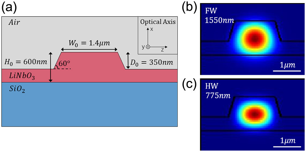
We investigate a set of LNOI ridge waveguides with the cross-section structure shown in Fig. 1(a). We utilize the commercial ion-sliced X-cut LNOI wafer (NANOLN) with a 600 nm LN film on a 2 µm silica with a 0.50 mm silicon substrate. The ridge waveguide is fabricated by dry etching with a top width of µ and an etching depth . As shown in Figs. 1(b) and 1(c), the optical mode profiles of fundamental transverse-electric (TE) modes at wavelengths of FW (1550 nm) and HW (775 nm) are simulated via the software of Lumerical Mode Solution. The simulated values of at FW and HW wavelengths are 1.915 and 2.104, respectively, and thus we can calculate the poling period to be about 4.1 µm. The TE-polarized modes used here correspond to type-0 quasi-phase matching (QPM) and utilize the highest second-order nonlinear tensor component of the X-cut LN film. Considering the potential phase-matching point shift caused by uniform dimension variation, we fabricate several identical LNOI ridge waveguides in parallel, with a 6 mm length to ensure the required SHG process. The poling periods range from 3.9 to 4.3 µm with an equal interval of 0.1 µm.
Figure 1.Structure and mode simulation of the LNOI waveguide. (a) Cross-section structure of the LNOI ridge waveguide (H, thickness; W, top width; D, etching depth). Optical mode profiles (energy density) for fundamental TE modes at (b) 1550 nm and (c) 775 nm.
The experimental setup is shown in Fig. 2. The sample is placed on an XYZ translation stage with temperature controlled at . A continuous-wave tunable telecom-band laser serves as the FW source. The laser light is emitted through a single-mode fiber with its polarization controlled by a polarization controller (PC). Then, the light is focused into the ridge waveguide at the front facet by an aspheric lens with a focal length of 4 mm. Another two aspheric lenses are placed at the waveguide end facet symmetrically to couple the output light into a multimode fiber with a short-pass filter to remove the FW light. The HW light is then measured by a high-sensitivity power meter. By simultaneously sweeping the wavelength of the laser and recording the HW light power, we are able to measure the SHG spectrum.
Figure 2.Experiment setup. A continuous-wave (CW) tunable laser serves as the FW source of the SHG process. The output HW light is measured by a high-sensitivity power meter (PM). Two polarizers are inserted to ensure QPM polarization. PC, polarization controller; MMF, multimode fiber.
In Figs. 3(a) and 3(b), we present two typical spectrum measurement results (blue curves) using two 6-mm-long waveguides with poling periods of 4.1 µm and 3.9 µm, respectively. Here, we focus on the SHG spectrum profile property, and, hence, we normalize the HW intensity by the total power of the whole spectrum. The spectrum shown in Fig. 3(a) exhibits one main single peak and several side peaks, and the main peak is fitted well with the sinc-square function (red curve) following Eq. (3), with the same bandwidth of about 4 nm. We can see that the experimental SHG conversion efficiency is about 75% of the theoretical value, and thus the side peaks do not influence the conversion efficiency. Such kind of spectrum was also reported in several experiments before[5,6]. In contrast, the spectrum shown in the upper part of Fig. 3(b) has several peaks without a specific main peak. Compared with the sinc-square function (red curve), the peaks are broadened up to 100 nm, and only less than 1% of theoretical conversion efficiency is measured. Moreover, as shown in Fig. 3(b), two simultaneous SHG processes of type-0 (upper) and type-I (lower) are simultaneously observed in the waveguide. By inserting corresponding polarizers in both the input and output of the waveguide, we observed type-0 and type-I SHG spectra, as shown in the upper and lower subfigures in Fig. 3(b) at near wavelengths, respectively.
Figure 3.Experimentally observed spectra (blue curves) from two 6-mm-long waveguides with poling periods of (a) 4.1 µm and (b) 3.9 µm, respectively. The red curves are plotted with sinc-square functions.
The non-ideal spectrum profiles may come from both poling and waveguide fabrication imperfections. However, the influence of waveguide dimension variations may be greater than that of the poling periodicity imperfections, due to the fact that the two types of errors are noise and Gaussian white noise[15]. Thus, here, we ignore the errors in poling and only consider the waveguide dimension variations. For simplicity, we fix the angle of the waveguide sidewall at 60° and consider the other three parameters of width, thickness, and etching depth, as independent variables.
The fabrication errors of waveguide width and etching depth come from the inductively coupled plasma (ICP) etching process. The absolute etching accuracy is about 100 nm in width dimension and 20 nm in etching depth, inducing dimension shift of designed values, with uniform offset within accuracy along the propagation direction. However, due to the incongruent etching rate of the central and side surfaces of the waveguide, inhomogeneous errors may also occur in etching depth dimension. We can estimate an inhomogeneous variation of less than 10 nm in etching depth by profilometer measurement. While for waveguide width, we can suppose the inhomogeneous errors are less than 5 nm, as inferred by the beam step size of electron beam lithography (EBL) in exposure. On the other hand, errors of thickness originate from LN film fabrication, which could be more inaccurate than waveguide etching. Actually, unlike waveguide width or etching depth, where inhomogeneous errors are more likely to act as short-range variation, the errors of thickness are also possibly long-range variations. Though minimum to 0.5 nm root mean square of roughness is already demonstrated after polishing, in the longer range, either gradient or stepped errors are possible with variation up to around 35 nm measured by the thin film thickness measurement system[18].
First, we focus on the phase-matching point shift. For the waveguides we used, central wavelengths of all of the observed spectra do not match the theoretically predicted ones, with deviations ranging from 50 nm to 150 nm. We simulate of FW and HW in the above waveguide structure by changing variables around the designed values, with the results shown in Fig. 4. We can see that changes are more sensitive to thickness variations than width and etching depth. By wavelength sweeping, the corresponding phase-matching points can be matched for 60 nm to 120 nm variation in width, or 10 nm to 25 nm variation in thickness. However, the required phase-matching point shift cannot be supported by changing the etching depth within deviations of 20 nm. Considering the practical fabrication deviation ranges we disuse before, we can infer that the phase-matching point shift mainly comes from the waveguide thickness deviations.
Figure 4.Simulated effective refractive index (Neff) as a function of (a) top width, (b) etching depth, and (c) thickness for all four waves in the waveguide.
The influence of waveguide thickness can be further evaluated from the arising of the type-I SHG process, as observed in Fig. 3(b). For the waveguide designed for type-0 SHG, the phase matching for both type-0 and type-I SHG processes cannot be satisfied simultaneously within up to 100 nm uniform deviations in waveguide width. However, by increasing the thickness of around 30 nm, simultaneous phase matching for both type-0 and type-I SHG processes can be achieved at nearby wavelengths.
In fact, the biggest obstacle for simultaneous phase matching of both type-0 and type-I processes results from the big gap of required poling periods due to the difference of TE and TM modes of FW. For waveguides, is determined by both material dispersion and structure. For shorter HW, of the TM mode is larger than that of the TE mode, which is mainly determined by the nature of the negative uniaxial crystal. While for longer FW, where the influence of the flat waveguide structure dominates, of TE becomes larger. The dimension variation may induce a greater change to of FW than to HW. As shown in Fig. 4(c), of the TM mode in FW becomes close to that of the TE mode as the thickness increases.
Then, we deal with the non-ideal spectrum profile. Following the method developed by Santandrea et al.[14], an average fidelity between the spectrum under inhomogeneous noise and the ideal one can be described by where is the noise amplitude and can be expressed as the product of the absolute partial derivative of phase mismatch and the fabrication error
Note that this method is not limited to dealing with waveguide imperfections. It can be applied to any noise with a single parameter noise that obeys spectrum density in the long-range correlation.
Considering the phase mismatch in Eq. (2) with a poling period fixed for ideal type-0 SHG in the original structure, the partial derivatives with respect to width, etching depth, and thickness can be calculated as µµµrespectively. Like sensitivities, the partial derivatives of thickness are also much larger than those of width and etching depth.
The fidelities between the measured SHG spectrum and the theoretically predicted one can be calculated by using the definition in Ref. [14], which all range from 0.75 to 0.17. This indicates that locates in the range of to , according to Eq. (4). Thus, we can infer that the imperfection corresponds to either 9 nm to 77 nm inhomogeneous errors in waveguide width, 11 nm to 95 nm in etching depth, or 1 nm to 9 nm in thickness. The estimated error scales for waveguide width and etching depth are not meaningful for practical fabrication accuracy. Hence, the non-ideal spectrum profiles are mainly caused by thickness variations.
Similarly, focusing on the non-trivial spectrum shown in Fig. 3(b), several peaks arise and greatly broaden the bandwidth. Such broadening is possibly caused by long-range errors in film thickness. For simplicity, here, we suppose a gradient change of thickness in the propagation direction. We can estimate a variation of about 16 nm by optimizing simulation of the spectrum fidelity, with the simulated result shown in Fig. 5. The broadened wavelength range is in good agreement with the simulation result, with the profile fidelity calculated as larger than 0.98. In addition to the long-range inhomogeneous thickness errors, short-range roughness could also have an influence here, indicated from the unfitted individual peaks. The optimized fidelity may be found with inhomogeneous variations of about 2 nm in width and etching depth or 0.2 nm in thickness. The above results all agree well with the fabrication accuracy discussed before.
Figure 5.SHG spectrum profile simulated with optimized gradient thickness change (red curve). The blue curve is the SHG spectrum measured in the experiment.
In conclusion, we explore the effect of dimension variation for the SHG process in LNOI in detail for the first time, to the best of our knowledge. By experimental SHG spectrum measurement and simulation on the waveguide dimension variations, we find that the SHG profile is most affected by the waveguide thickness variation. We estimate a uniform deviation of about 30 nm or inhomogeneous errors of about 16 nm on waveguide thickness, which are both reasonable in fabrication. The work can be useful to evaluate fabrication performance of LNOI-based nonlinear optical devices and help to approach higher experimental performance as theoretically predicted in the future.
References
[1] Y. Qi, Y. Li. Integrated lithium niobate photonics. Nanophotonics, 9, 1287(2020).
[2] D. Sun, Y. Zhang, D. Wang, W. Song, X. Liu, J. Pang, D. Geng, Y. Sang, H. Liu. Microstructure and domain engineering of lithium niobate crystal films for integrated photonic applications. Light Sci. Appl., 9, 197(2020).
[3] J. Lin, F. Bo, Y. Cheng, J. Xu. Advances in on-chip photonic devices based on lithium niobate on insulator. Photon. Res., 8, 1910(2020).
[4] Y. Jia, L. Wang, F. Chen. Ion-cut lithium niobate on insulator technology: recent advances and perspectives. Appl. Phys. Rev., 8, 011307(2021).
[5] L. Chang, Y. Li, N. Volet, L. Wang, J. Peters, J. E. Bowers. Thin film wavelength converters for photonic integrated circuits. Optica, 3, 531(2016).
[6] C. Wang, C. Langrock, A. Marandi, M. Jankowski, M. Zhang, B. Desiatov, M. M. Fejer, M. Lončar. Ultrahigh-efficiency wavelength conversion in nanophotonic periodically poled lithium niobate waveguides. Optica, 5, 1438(2018).
[7] Y. Niu, C. Lin, X. Liu, Y. Chen, X. Hu, Y. Zhang, X. Cai, Y.-X. Gong, Z. Xie, S. Zhu. Optimizing the efficiency of a periodically poled LNOI waveguide using in situ monitoring of the ferroelectric domains. Appl. Phys. Lett., 116, 101104(2020).
[8] Y. Liu, X. Yan, J. Wu, B. Zhu, Y. Chen, X. Chen. On-chip erbium-doped lithium niobate microcavity laser. Sci. China Phys. Mech. Astron., 64, 234262(2021).
[9] L. Ge, Y. Chen, H. Jiang, G. Li, B. Zhu, Y. Liu, X. Chen. Broadband quasi-phase matching in a MgO:PPLN thin film. Photon. Res., 6, 954(2018).
[10] M. M. Fejer, G. A. Magel, D. H. Jundt, R. L. Byer. Quasi-phase-matched second harmonic generation: tuning and tolerances. IEEE J. Quantum Electron., 28, 2631(1992).
[11] S. Helmfrid, G. Arvidsson, J. Webjörn. Influence of various imperfections on the conversion efficiency of second-harmonic generation in quasi-phase-matching lithium niobate waveguides. J. Opt. Soc. Am. B, 10, 222(1993).
[12] J. S. Pelc, C. R. Phillips, D. Chang, C. Langrock, M. M. Fejer. Efficiency pedestal in quasi-phase-matching devices with random duty-cycle errors. Opt. Lett., 36, 864(2011).
[13] D. Chang, C. Langrock, Y.-W. Lin, C. R. Phillips, C. V. Bennett, M. M. Fejer. Complex-transfer-function analysis of optical-frequency converters. Opt. Lett., 39, 5106(2014).
[14] M. Santandrea, M. Stefszky, C. Silberhorn. General framework for the analysis of imperfections in nonlinear systems. Opt. Lett., 44, 5398(2019).
[15] M. Santandrea, M. Stefszky, V. Ansari, C. Silberhorn. Fabrication limits of waveguides in nonlinear crystals and their impact on quantum optics applications. New J. Phys., 21, 033038(2019).
[16] M. Santandrea, M. Stefszky, G. Roeland, C. Silberhorn. Characterisation of fabrication inhomogeneities in Ti:LiNbO3 waveguides. New J. Phys., 21, 123005(2019).
[17] R. J. A. Francis-Jones, P. J. Mosley. Characterisation of longitudinal variation in photonic crystal fibre. Opt. Express, 24, 24836(2016).