
Yaobin Li, Ming Li, pingping Qiu, Weinian Yan, Ruiwen Jia, Qiang Kan. Design of High Power Low Loss 852 nm Fabry-Perot Laser[J]. Laser & Optoelectronics Progress, 2022, 59(3): 0314001
- Laser & Optoelectronics Progress
- Vol. 59, Issue 3, 0314001 (2022)
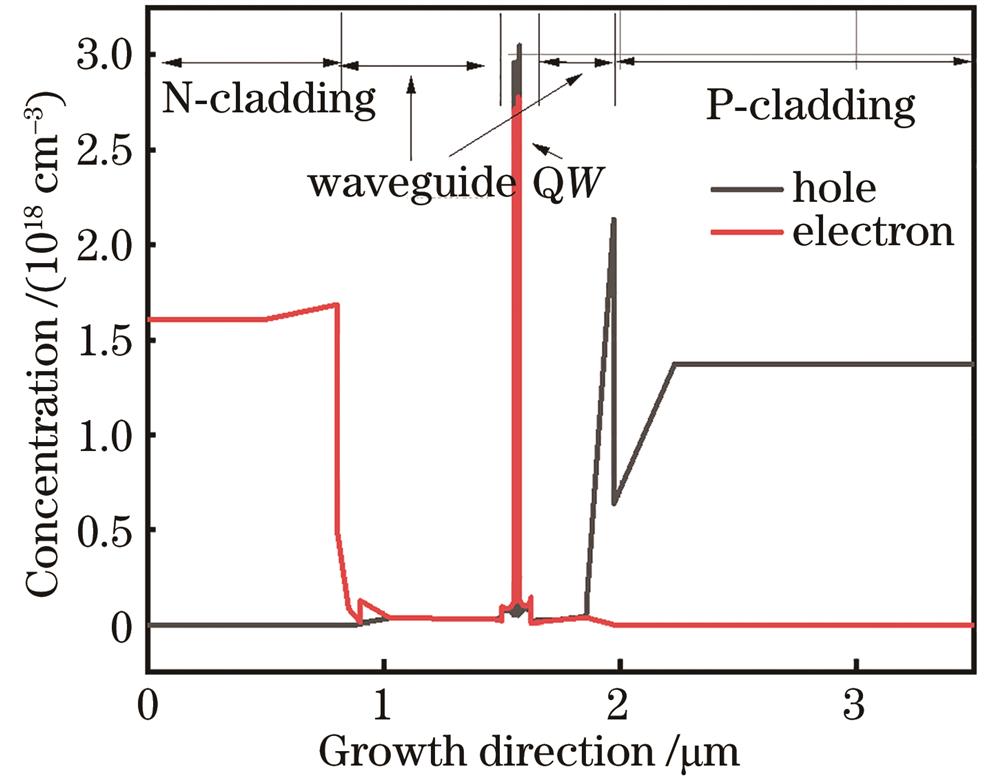
Fig. 1. Carrier concentration distribution of the laser at 500 mA injection current
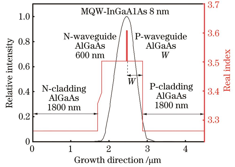
Fig. 2. Field distribution and effective refractivity parameter of laser
Fig. 3. Internal loss changes with W of the P-waveguide layer, doping concentration of P-cladding layer, and waveguide layer
Fig. 4. Schematic for optimizing doping concentration in waveguide and laser structures
Fig. 5. Simulation of electron and hole concentration distributions of lasers with different structures at same injection current. (a) Electron concentration distribution; (b) hole concentration distribution
Fig. 6. Current density distributions in vertical direction. (a) Electron; (b) hole
Fig. 7. Experimental results. (a) Internal loss and internal quantum efficiency versus doping concentration of P-cladding layer; (b) internal loss and internal quantum efficiency versus Al composition of different AlXGa1-XAs materials
Fig. 8. Room temperature PL spectrum of FP laser
Fig. 9. Spectrogram of FP laser
Fig. 10. Cross section of the FP laser
Fig. 11. Relationship between cavity length and inverse external differential efficiency
Fig. 12. Experimental and theoretical results of optical and electrical characteristics
Fig. 13. Current density distribution diagrams with different structures in epitaxial direction. (a) Electron; (b) hole
Fig. 14. Far-field test results. (a) Direction of divergence angle of fast axis; (b) direction of divergence angle of slow axis

Set citation alerts for the article
Please enter your email address
© Copyright 2018-2021 | Chinese Laser Press. All Rights Reserved 沪ICP备15018463号-20