• Journal of Semiconductors
  • Vol. 40, Issue 11, 111605 (2019)
Donghwi Cho1, Junyong Park2, Taehoon Kim1、3, and Seokwoo Jeon1
Author Affiliations
  • 1Department of Materials Science and Engineering, KAIST Institute for the NanoCentury, Korea Advanced Institute of Science and Technology (KAIST), Daejeon 34141, Republic of Korea
  • 2School of Materials Science and Engineering, Kumoh National Institute of Technology, Gumi, Gyeongbuk 39177, Republic of Korea
  • 3Department of Biomedical Engineering, Tufts University, Medford, Massachusetts, 02155, USA
  • show less
    DOI: 10.1088/1674-4926/40/11/111605 Cite this Article
    Donghwi Cho, Junyong Park, Taehoon Kim, Seokwoo Jeon. Recent advances in lithographic fabrication of micro-/nanostructured polydimethylsiloxanes and their soft electronic applications[J]. Journal of Semiconductors, 2019, 40(11): 111605 Copy Citation Text show less

    Abstract

    The intensive development of micro-/nanotechnologies offers a new route to construct sophisticated architectures of emerging soft electronics. Among the many classes of stretchable materials, micro-/nanostructured poly(dimethylsiloxane) (PDMS) has emerged as a vital building block based on its merits of flexibility, stretchability, simple processing, and, more importantly, high degrees of freedom of incorporation with other functional materials, including metals and semiconductors. The artificially designed geometries play important roles in achieving the desired mechanical and electrical performances of devices and thus show great potential for applications in the fields of stretchable displays, sensors and actuators as well as in health-monitoring device platforms. Meanwhile, novel lithographic methods to produce stretchable platforms with superb reliability have recently attracted research interest. The aim of this review is to comprehensively summarize the progress regarding micro-/nanostructured PDMS and their promising soft electronic applications. This review is concluded with a brief outlook and further research directions.

    1. Introduction

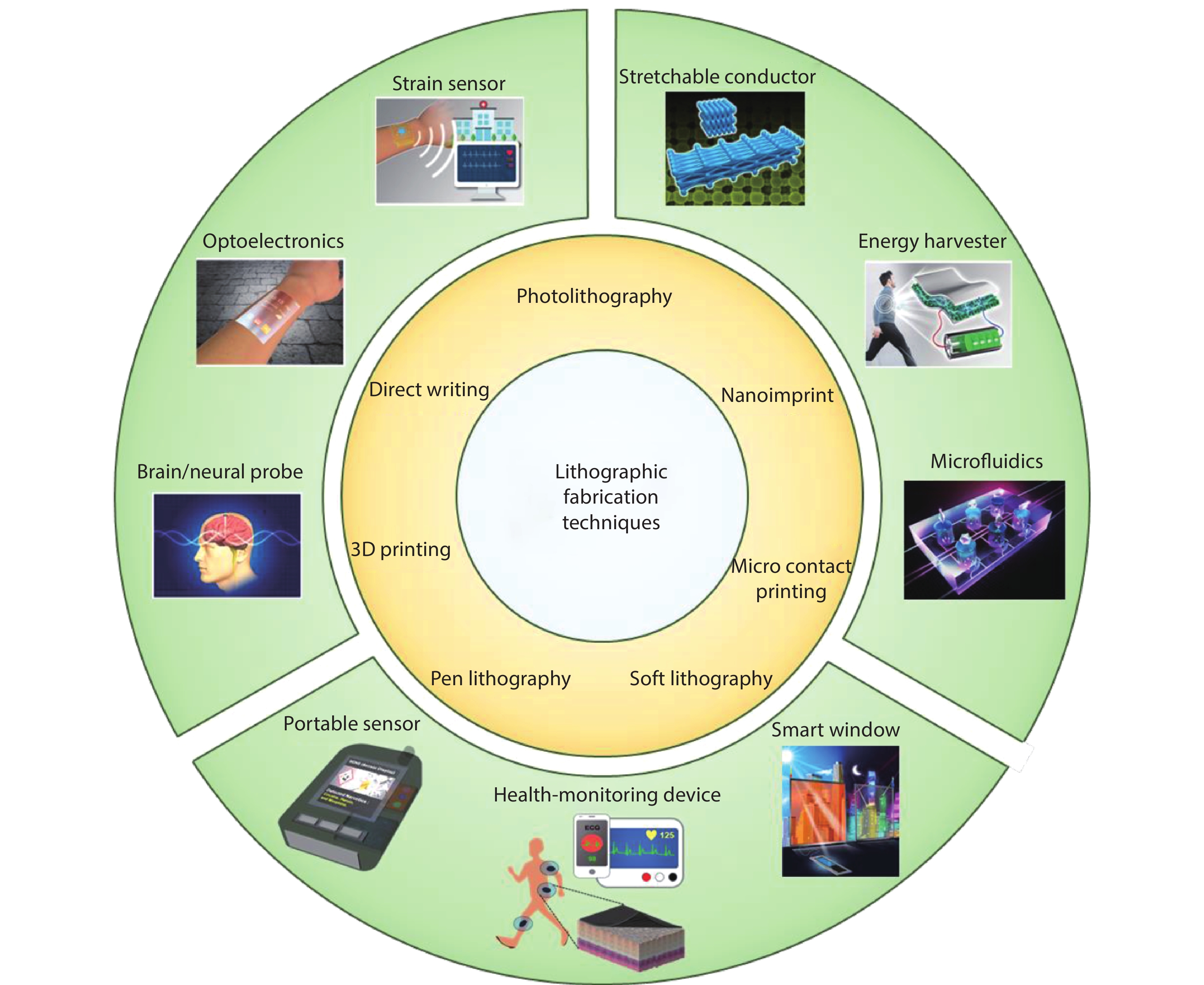
    As micro- and nanoelectromechanical system (MEMS/NEMS) technologies have been rapidly developed, soft electronics are opening new a paradigm in human-machine interfaces[1-7]. Emerging soft electronics necessarily involve stretchable conductors interconnected with various types of sensors[8, 9], actuators[10, 11] and many other optoelectronic devices[12-14] and can be exploited for a variety of practical purposes such as health monitoring[15, 16], clinical applications[17, 18], and wearable communication devices[19-22] through flexible/stretchable forms of electronics (Fig. 1). In all instances, their electrodes must meet two major prerequisites to realize levels of flexibility and stretchability. One is the compatibility of substrates with established conducting pathways comprised of inorganic materials under large strains ( %), and the other is full-recovery to their initial states without performance degradation after releasing the applied strain[1, 23]. Thus, it is easy to understand that fundamental approaches based on material designs for stretchable electrodes not only determine the mechanical and electrical performances of the resulting soft electronic devices but also offer many advantageous features in terms of system designs, user interfaces, and unique functionalities beyond their inherent characteristics.

    (Color online) An overview figure of the lithographic fabrication techniques and their applications. Strain sensor image, optoelectronics image, and brain/neural probe image: Reprinted from Ref. [1]. Copyright 2019 The Royal Society of Chemistry. Smart window image: Reprinted from Ref. [146]. Copyright 2018 Nature Publishing Group. Microfluidics image: Reprinted from Ref. [147]. Copyright 2019 The Royal Society of Chemistry. Stretchable conductor image: Reprinted from Ref. [23]. Copyright 2018 Nature Publishing Group.

    Figure 1.(Color online) An overview figure of the lithographic fabrication techniques and their applications. Strain sensor image, optoelectronics image, and brain/neural probe image: Reprinted from Ref. [1]. Copyright 2019 The Royal Society of Chemistry. Smart window image: Reprinted from Ref. [146]. Copyright 2018 Nature Publishing Group. Microfluidics image: Reprinted from Ref. [147]. Copyright 2019 The Royal Society of Chemistry. Stretchable conductor image: Reprinted from Ref. [23]. Copyright 2018 Nature Publishing Group.

    To date, there have been many efforts to achieve stretchable electrodes by constructing conductive percolation networks on/in elastomeric films[15-18, 21, 23-27]. Representative examples of stretchable electrodes have been created to be intimately integrated with compliant substrates through accommodating the applied strain (ε) induced on patterned percolation pathways such as serpentine-shaped[28] or coil-like conductive films of metal[29, 30], conductive oxides[31-33], and carbon-based materials[24-26]. Despite the significant technical developments, the resulting performances are limited by fundamental mismatches between the conducting materials and the substrates and the intrinsically low stretchability of the electronic materials. To address this critical issue, researchers have been devoted to finding a breakthrough in sophisticated embodiments in terms of accommodating the applied strain, including pre-strained surface wavy shapes[34-37], in-plane mesh geometries[25, 26], and three-dimensional (3D) buckling structures[24, 38]. These strategies of directly employing the structures in the substrates have been presented to effectively dissipate the mechanical fracturing of stretchable electrodes under external strains including bending, stretching, twisting and deforming into curvilinear shapes while maintaining the electronic performance.

    Among the many classes of elastic foam materials, silicon-based organic elastomers, especially polydimethylsiloxane (PDMS) have received intensive research interest as vital building blocks[39-41]. PDMS is a viscoelastic, biocompatible, mechanically and chemically robust elastomer with high cost-effectiveness, which is highly advantageous for further practical applications[39]. In particular, the intrinsic flexible and hydrophobic siloxane chains (Si–O–Si) of PDMS provide not only superb elasticity and water-proof property but also high degrees of freedom in its moldability[42]. From the perspective of material engineering, the feasible processability of PDMS plays a critical role in achieving high-performance wearable electronic applications such as stretchable conductors[1, 8, 16, 23], sensors and actuators[4, 24] and bio-sensor platforms[15] and in extending the research scope to realize new functions[39-41] from sophisticated embodiments. The stretchability of the electronic devices, which is one of the primary goals of current research, is not only determined by the inherent material properties such as the elastic modulus, viscoelasticity, and molecular structure but also significantly enhanced by the physical structure of the material[23, 24]. In comparison with non-structured materials, structural layouts providing additional deformation freedom offer lower densities and higher surface areas and contribute extraordinary deformability and elasticity. Structure-motivated approaches, for example, the generation novel structural designs ranging from 2D planar structures of periodic lines and wavy structures[43-46] to 3D engineered micro-/nanopillars and porous networks[23, 24], have greatly extended the stretchability beyond the given material properties. More importantly, the introduction of finely controlled micro-/nanostructures to PDMS to achieve tunable material properties through adjusting the morphology including the geometry, dimension, and porosity not only produces a flexibly deformable platform but also offers an optimal scaffold for constructing electrical pathways[24]. These properties are attributed to the potential to combine the controlled mechanical properties of the physical structure of the PDMS with the electrical properties of the incorporated functional materials such as metals[29, 30, 46], inorganic conductors[31-33], and carbon-based materials[24-26, 47]. Despite the promising capabilities of these materials, chemistry-based fabrication methods generally hinder the reliable production of structures, resulting from the required complicated processes and technical constraints on the precise adjustment of the morphologies. On the other hand, it has recently been reported that this issue can be overcome by means of soft lithographic techniques[1, 4]. The well-known route is to utilize patterning, molding and imprinting techniques that can finely adjust the geometric parameters of the structured PDMS via MEMS/NEMS technologies[48]. Additionally, with advances in well-developed wafer-based systems, the reproducibility and scalability has been greatly improved, and state-of-art lithographic technologies offer new design opportunities to develop structures[37]. Considering their remarkable contribution to the improvement of the overall performances of stretchable electronics and accelerating the growth of research interest, a critical review that summarizes recent progresses in fabrication methods of structured PDMS with various architectures and the associated promising applications can trigger further research interest.

    In this review, we aim to provide an overview of the comprehensive lithographic technologies used to produce micro-/nanostructured PDMS, as well as their soft electronic applications such as in stretchable displays, sensors, and bio-sensor platforms and showcase intriguing demonstrations of structural effects. This review begins with a brief introduction to representative fabricating strategies for structured PDMS, and a discussion of their advantages and drawbacks follows. Afterwards, the roles of structured PDMS in various applications are considered, and finally, this review is concluded with personal intuition towards existing technical challenges and a forecast of further research directions.

    2. Fabrication methods of micro-/nanostructured PDMS

    2.1. Photolithography with PDMS etching procedures

    The demand for PDMS as the structural material in MEMS/NEMS technologies has explosively increased due to its excellent structural resolution and accuracy of less than 10 nm[49]. While this material has the advantage of being applicable in most processing technologies, PDMS has been found to be incompatible with conventional lithographic techniques because of its low surface energy, which results in poor coverage of photoresists on the PDMS surface and adhesion problem[50, 51]. At the initial research stage, Ryu et al. reported a simple route to pattern PDMS into a 2D structure through physically removing the excessive PDMS prepolymer from the pre-structured mold at the micron scale with a traversing blade[50]. This mechanical etching process generally suffers from limited resolution of patterns and, more importantly, poor uniformity and tapered edge profiles resulting from the uncontrolled interfaces between the mold and PDMS. These issues originating from the intrinsically hydrophobic surface can be overcome by simple treatment of the PDMS surface with O2 plasma or ozone[24, 52, 53]. This surface modification creates a relatively hydrophilic surface by inducing methyl groups on the PDMS surface and spontaneously generating silanols[54]. With this significant attribute, soft lithography, which is a simple yet highly precise and repeatable method, offers a rational route to precisely control the morphology of PDMS. Chenet al. reported a PDMS surface micromachining technique utilizing direct photolithography followed by reactive-ion etching (RIE)[51]. The overall fabrication process is demonstrated in Fig. 2(a). The easily implementable surface micromachining technique at the wafer level can be integrated with other conventional microfabrication techniques and is applicable to produce microstructured PDMS in various planar structures. In-plane perforations of PDMS membranes defined by the micromachining method are shown in Figs. 2(b)2(f). The microstructured PDMS membranes are designed to have thicknesses of 2 to 20 mm with hexagonal and square arrays. In addition, free-standing thin PDMS beam structures on Si wafer substrates with a thickness of 500 nm and a total beam length of 800 μm have been fabricated. As shown in Figs. 2(g)2(j), the beam widths were 2, 10, and 5 μm, respectively. This result indicates that wafer-level fabrication provides a new design opportunity for 2D planar PDMS structures ranging from submicrons to tens of micrometers in size.

    (Color online) Lithographic surface micromachining of PDMS. (a) Schematic illustrations of photolithographic surface micromachining of PDMS. (b–j) Free-standing PDMS microfiltration membranes and beam structures. (b–f) SEM images of the microstructured PDMS membrane bonded to (e) a PDMS support structure. The membrane had a thickness of 10 μm, and it contained an array of hexagonally spaced through-holes (with a hole diameter of 4 μm). (g–j) Free-standing PDMS beam structures on Si wafer substrates, with the beam thickness of 500 nm and a total beam length of 800 μm. The minimum beam widths were (g) 2 μm, (h) 10 μm, and (i, j) 5 μm, respectively. (Reprinted from Ref. [51]. Copyright 2012 The Royal Society of Chemistry.)

    Figure 2.(Color online) Lithographic surface micromachining of PDMS. (a) Schematic illustrations of photolithographic surface micromachining of PDMS. (b–j) Free-standing PDMS microfiltration membranes and beam structures. (b–f) SEM images of the microstructured PDMS membrane bonded to (e) a PDMS support structure. The membrane had a thickness of 10 μm, and it contained an array of hexagonally spaced through-holes (with a hole diameter of 4 μm). (g–j) Free-standing PDMS beam structures on Si wafer substrates, with the beam thickness of 500 nm and a total beam length of 800 μm. The minimum beam widths were (g) 2 μm, (h) 10 μm, and (i, j) 5 μm, respectively. (Reprinted from Ref. [51]. Copyright 2012 The Royal Society of Chemistry.)

    2.2. Direct patterning of PDMS

    Previous lithographic technologies using PDMS have significantly relied on additional direct etching procedures such as RIE processes and mechanical scrapping with sharp edges. In spite of their active removal processes, it is difficult to achieve precise control of the morphology because of the unavoidable PDMS residue left behind[51]. To solve this issue, much effort has been devoted to making PDMS photosensitive and photo-patternable[51, 54-57]. For example, Ward et al. successfully demonstrated a photo-patterning approach by adding photo-initiators such as benzophenone or 2,2-dimethoxy-2-phenylacetophenone (DMAP) into the PDMS matrix[56-58]. Likewise, the conventional negative-tone photoresists, the UV-exposed regions in the PDMS, survived after the development steps. Although the novel strategy involves one lithographic step of preparation to produce structured PDMS, the photo-initiating chemicals generally require extensive care to maintain the controlled state under a minimized amount of oxygen existing in the PDMS, as it serves as an inhibitor of photo-crosslinking during the UV exposure[59]. With the increasing attention to this simple technical approach, Dow Corning and others released a series of commercial products as photo-patternable PDMS[60-62]. For example, photo-patternable silicone was presented, which can be directly patterned by following the well-known lithographic fabrication steps including spin casting, soft baking, UV exposing, post baking, developing, rinsing and hard baking. This material is advantageous for integration with well-established MEMS technologies, but still, some drawbacks such as high costs and limited processing conditions need to be addressed. Bhagat et al. suggested alternatives to the aforementioned techniques by synthesizing a photo-definable PDMS which is only sensitive to light below 365 nm due to the absorption spectrum of benzophenone with peaks at 260 nm[57]. The authors claimed that the developed materials are free from processing under normal ambient light, which greatly contributes to extending the environmental conditions beyond the conventional yellow room. Fig. 3(a) illustrates the photo-definable PDMS process sequences, and Fig. 3(b) shows two Y-junction microfluidic channel patterns with feature sizes ranging from 100 μm to several millimeters. Unlike the previous results from the traditional replication of PDMS from molds or masters, the results were directly patterned. In addition, the pattern resolution can be improved to the dozens-of-microns scale, and dual-layered structures can also be prepared through two-step photolithographic steps. As shown in Figs. 3(c) and 3(d), finely controlled examples are demonstrated in a 30 μm-thick patterned free-standing film with a variety of feature sizes from 0.5 to 2 mm. Despite the development of a simpler, cheap, and rapid way to produce the microstructured PDMS, the levels of pattern resolution are limited to only the micron scale due to the chronic bottleneck of requiring a certain distance when the photomask is applied in UV exposure[51]. In turn, to utilize the novel features of more sophisticated 3D structures through these fabrication methods, the complex and time consuming manufacturing procedures of layer-by-layer strategies should be followed.

    Microstructuring technique with photopatternable PDMS. (a) Schematic illustrations of the photoPDMS process sequence. (b) SEM image of a 400 μm-wide channel with 200 μm inlets. The image shows vertical channel walls similar to those achieved using conventional photoresists. (c) Photograph of a 30 μm-thick patterned free-standing photoPDMS film with various feature sizes from 0.5 to 2 mm. (d) Digital image of a dual-layered photoPDMS structure fabricated using a two-step lithography process. (Reprinted from Ref. [57]. Copyright 2007 The Royal Society of Chemistry.)

    Figure 3.Microstructuring technique with photopatternable PDMS. (a) Schematic illustrations of the photoPDMS process sequence. (b) SEM image of a 400 μm-wide channel with 200 μm inlets. The image shows vertical channel walls similar to those achieved using conventional photoresists. (c) Photograph of a 30 μm-thick patterned free-standing photoPDMS film with various feature sizes from 0.5 to 2 mm. (d) Digital image of a dual-layered photoPDMS structure fabricated using a two-step lithography process. (Reprinted from Ref. [57]. Copyright 2007 The Royal Society of Chemistry.)

    2.3. PDMS replication from a 3D template via unconventional lithography

    With the recent development of a variety of new 3D patterning technologies through non-traditional methods, the high-level engineering of elaborate 3D architectures and the fundamental understanding of these structures through in-depth studies have been considered as breakthroughs for a wide range of existing applications over the fields of energy storage devices[63, 64], microfluidics[65-67], photonics[67-75], and, especially, electronics[15, 23, 24]. As mentioned in the introduction, the emphasis here is on micro-/nanostructured PDMS, and representatives based on lithographic fabrications are discussed in the following subsections. A straightforward method which is generally utilized for generating the structured PDMS includes the use of various types of templates such as sugar cube, PS beads, Ni foam, etc[39]. In particular, one of the critical limitations of previous approaches is the feasibility of scale-down to the nano dimension with uniformity. In this section, a powerful technology for the production of finely designed 3D micro-/nanostructures is introduced. The well-known principle is to replicate the structures from solid templates, which is defined by unconventional 3D lithographic technologies. This direct templating method is highly advantageous for generating not only planar structures but also more complex 3D architectures at both the micron and nano scales.

    2.3.1. Interference lithography

    The use of multi-beam interference lithography offers a rational design opportunity to fabricate well-established 3D structures at the submicron scale[57, 65, 76-81]. Interference lithography (IL) is one of the unconventional photolithography techniques which can directly transfer a periodically generated 3D light distribution into a photoresist. This method is highly advantageous for controlling structural factors such as the porosity, symmetry, and dimension by adjusting optical parameters such as the wavelength, incident angle, intensity and many others. In the case of using a positive-tone photoresist, for example, regions with destructive interference form the structure, and the other regions are selectively removed after the development procedure[23, 78]. To utilize the novel characteristics of 3D nanostructures including large surface areas[24, 63, 64, 71, 74, 75], porosities[71, 74, 75], and mass transportation abilities[63, 82, 83], fabricated 3D nanostructures are generally exploited to serve as templates for transforming the polymeric material into various functional materials, such as metals[23, 82, 84], ceramics[63, 64, 66, 71, 75], semiconducting materials and some organic materials[15, 23, 24, 73]. Thus, it is obvious that the removability of the 3D template directly determines the capability of material conversion. Considering this governing factor, there have been numerous efforts to transfer 3D nanostructures to functional organic materials, especially for PDMS due to its potential swelling issue during the template removal process of photolithographic technologies[15, 23, 24, 78, 80]. The most commonly used commercial photoresist is SU-8, which is based on an epoxy and generally requires harsh removal processes such as heat treatment at up to 500 °C and a plasma etching step[23, 24]. From the point view of material conversion, available materials are significantly limited to only metals and ceramics which have heat and chemical resistance and do not include organic materials. Recently, Jang et al. reported a new route for removing the 3D template in a bicontinuous 3D network and conveniently replicated the topological interconnections without structural degradation[78]. A positive-tone photoresist (AZ5214-E, MicroChemicals) was used to prepare the 3D template through the IL technique, and after infiltration of the PDMS prepolymer into the interconnected pores of the template, the photoresist was selectively removed in an aqueous solution appropriate for removing it without PDMS swelling or pattern collapse. The 3 steps of the fabrication procedure for 3D elastomeric network/air materials are illustrated in Fig. 4(a). In the first step, a 3D ILT is prepared via the IL technique. The porous 3D ILT is completely filled with the PDMS prepolymer with the assistance of vacuum infiltration, and the PDMS is cured via thermal treatment. Finally, a second flood exposure to UV light makes the 3D template easily soluble in the aqueous remover. With the knowledge that PDMS is subject to a swelling problem from nonpolar organic solvents such as hexane, chloroform, acetone, and even ethanol, the development of a template removal process using a water-based solution has been found to be a cheap and rapid way to produce the periodic 3D nanostructure of PDMS[24, 85]. As a result, as shown in Figs. 4(b) and 4(c), theoretical light intensity models and reconstructed confocal micrographs prove a reasonable correspondence of the technique with the optical calculation. Consequently, an interconnected PDMS network with periodicity at the submicron scale is successfully constructed, as shown in Fig. 4(d). From the perspective of utilizing the synergetic effects between the structural advantages (which generally include the porosity, high surface area, and functional geometry) and intrinsic features of PDMS elastomers, as discussed in the introduction, technologies need to be developed to achieve reliable production with practically large areas, which will ensure significantly improved performances of existing applications[39].

    (Color online) Fabrication of 3D elastomeric network/air structures via interference lithography. (a) Schematic illustration of the fabrication process. (b) Theoretical light intensity model. The brown and green colors indicate the inner and outer surfaces, respectively. (c) Reconstructed confocal image showing a perspective view of the PDMS elastomeric structure. (d) SEM images of the prepared 3D PDMS network/air structure. (Reprinted from Ref. [78]. Copyright 2006 American Chemical Society.)

    Figure 4.(Color online) Fabrication of 3D elastomeric network/air structures via interference lithography. (a) Schematic illustration of the fabrication process. (b) Theoretical light intensity model. The brown and green colors indicate the inner and outer surfaces, respectively. (c) Reconstructed confocal image showing a perspective view of the PDMS elastomeric structure. (d) SEM images of the prepared 3D PDMS network/air structure. (Reprinted from Ref. [78]. Copyright 2006 American Chemical Society.)

    2.3.2. Proximity-field nanopatterning (PnP)

    The PnP technique is an advanced 3D nanofabrication technology that utilizes high-resolution, conformable phase masks and provides a powerful route to produce classes of 3D nanostructures[15, 23, 24, 54, 63-75, 82-84, 86-89]. With single exposure through the conformal phase mask that contains periodic relief structures with a comparable feature size to the incident wavelength, the diffracted beams generated from the periodic relief structures of the phase mask induce constructive and destructive interferences and create a 3D distribution of intensity, which is called the Talbot effect. In brief, the PnP technique uses this intriguing optical phenomenon as an unconventional 3D nanopatterning technique. The PnP technique is advantageous for producing large-area 3D nanostructures. These structures generally serve as polymeric templates for conversing into various functional materials such as metals, oxides, semiconductors, and polymers. The well-known methods include depositing the functional materials on the surface of the template or infiltrating into the pores of the structure and removing the template. In turn, the capability of the flexible material conversion with superb scalability over inch scale offers one promising lithographic strategy to generate a variety of architectures. In particular, PnP can also provide highly periodic 3D templates to produce nanostructured PDMS by removing the 3D polymeric templates with the mild solvents. For example, Park et al. proposed a new fabrication method for producing 3D nanostructured PDMS, which the authors refer to as 3D PDMS[23]. As shown in Fig. 5(a), the process began with the preparation of the 3D template defined by the PnP technique. A positive-tone photoresist (AZ-9260, Clariant) was used to provide an easily removable template (Fig. 5(b)). After following the conventional patterning processes using the positive-tone photoresist, an additional AZ-9260 thin film placed on the substrate as sacrificial layer provided a way to make the 3D PDMS spontaneously release as a free-standing film by first being removed by the buffered aqueous solution of KOH after infiltration of the PDMS prepolymer, without any structural damage (Fig. 5(c)). A key advancement over previous works is the great extension of the pattern thickness of the resulting 3D nanostructure with the positive resist. Most positive resists possess high absorption coefficients and are significantly restricted in achieving levels of thickness higher than 3 μm by utilizing 3D nanopatterning techniques[23, 78]. This issue can be overcome by a unique optical property of DNQ-based resists, which is known as the photo-bleaching effect. As the UV light exposure time increases, the original chemical system changes into indene-carboxylic acid photoproducts and becomes an optically new material with a relatively reduced absorption. Accordingly, the pattern thicknesses that can be achieved are significantly extended from 3 to 10 μm. The free-standing 3D PDMS film maintains its 3D continuous porous nanonetwork with the mechanical assistance of the conformal backing PDMS layers, as shown in Fig. 5(d). On the basis of the MEMS photolithographic advantages, the produced coverage is not limited to bulk volumes and can also be designed as arbitrary shapes by performing 2-step photolithography using a multiple-photomask system. The resulting 3D PDMS films with line and space patterns are shown in Fig. 5(e). In turn, the 3D PDMS can be applied as a porous elastomeric scaffold for various applications, especially stretchable electrode systems. This application will be discussed in the following sections.

    (Color online) Fabrication of highly ordered, 3D nanostructured PDMS by the proximity-field nanopatterning (PnP) technique and material conversion technique. (a) Schematic illustration of the fabrication procedures to produce 3D PDMS. (b) Top-view SEM image of the top surface of the 3D polymeric template, which was fabricated with a positive-tone photoresist, after intentionally removing part of the first layer and (c) the replicated 3D PDMS from the template. (d) Optical image of a supported 3D PDMS film and (e) a folded 3D PDMS film with line patterns (scale bar = 1 cm) (Reprinted from Ref. [23]. Copyright 2012 Nature Publishing Group.) (f) Top-view SEM image of the top surface of the 3D polymeric template, which was fabricated with a negative-tone photoresist and (g) the resulting 3D PDMS. (Reprinted from Ref. [24]. Copyright 2017 American Chemical Society.)

    Figure 5.(Color online) Fabrication of highly ordered, 3D nanostructured PDMS by the proximity-field nanopatterning (PnP) technique and material conversion technique. (a) Schematic illustration of the fabrication procedures to produce 3D PDMS. (b) Top-view SEM image of the top surface of the 3D polymeric template, which was fabricated with a positive-tone photoresist, after intentionally removing part of the first layer and (c) the replicated 3D PDMS from the template. (d) Optical image of a supported 3D PDMS film and (e) a folded 3D PDMS film with line patterns (scale bar = 1 cm) (Reprinted from Ref. [23]. Copyright 2012 Nature Publishing Group.) (f) Top-view SEM image of the top surface of the 3D polymeric template, which was fabricated with a negative-tone photoresist and (g) the resulting 3D PDMS. (Reprinted from Ref. [24]. Copyright 2017 American Chemical Society.)

    Recently, Cho et al. reported that the 3D nanostructure defined by the PnP using a negative-tone photoresist can also be an appropriate 3D template for conversion to PDMS[24]. In general, as discussed in the lithographic technique sections, most negative-tone photoresists are epoxy-based polymers or off-stoichiometry thiol-ene (OSTE) polymers which require harsh removal steps such as high-temperature burning above 500 °C or plasma etching, along with toxic organic solvents[90]. However, a phenolic-based negative-tone photoresist (NR5, futurrex) has newly been employed to fabricate 3D templates for producing 3D PDMS. The NR5 can be easily removed by a single drop of dimethyl sulfoxide (DMSO), which produces the lowest swelling ratio of PDMS (similar to that of water)[91]. Following the PnP steps with a 355 nm laser provides successful preparation of a 3D template with a periodicity of 600 nm and pore diameters of approximately 300 nm, which is the inverse structure of the 3D nanostructure with the positive-tone photoresist (Fig. 5(f)). After removing the template, 3D PDMS is obtained without severe structural degradation, as shown in Fig. 5(g). The detailed diameter and porosity of the 3D nanostructure significantly depend on the optical values of the photoresist including the refractive index and level of pattern resolution. In turn, the resulting 3D PDMS has slightly different feature sizes compared to that from the positive-tone photoresist AZ-9260. The 3D PDMS from NR5 has a periodicity of 3.1 μm in the z-direction, which is relatively longer than that of the 3D PDMS from AZ-9260 (with an approximate periodicity of 2.2 μm). It has been found that the development of 3D PDMS fabrication methods greatly contributes to not only improving the stretchability of soft electronics but also achieving other functional behaviors by incorporating new structural functions from other functional materials. The further research direction of the PnP method includes 1) scalability beyond the wafer scale, 2) extending the range of the designable structures from periodic structures to arbitrary structures, and 3) realization of the thick-pattern over 50 μm which is limited by the intrinsic light absorption of the photoresist. To improve the quality of the various applications based on the 3D PDMS, the aforementioned issues should be solved.

    2.4. 3D printing technique

    Additive manufacturing, also known as 3D printing techniques, has drawn tremendous attention due to its extraordinarily high freedom of producing intricate or arbitrary architectures[92-99]. This intuitive, mold-free fabrication technique has evolved to realize new characteristics and improved properties from the micron scale to the bulk scale. According to these attributes, many efforts to 3D print PDMS have recently been reported[100-102]. Still, there are some technical issues with reliably generating 3D-printed PDMS due to the liquid nature of the PDMS precursor, which has a low elastic modulus, and its crosslinking mechanism. One of the well-known routes for constructing various physical structures with PDMS is to make the silicone precursor a non-flowable or thixotropic fluid by incorporating additives that help the PDMS prepolymer be cured even under low temperatures, preserving the geometric accuracy during the curing step[93, 94, 99]. For instance, Lv et al. proposed that the addition of silica nanoparticles into PDMS can provide improved mechanical strength of the ink for PDMS 3D printing[97]. The hydrophobic nanosilica-filled PDMS ink ensures the construction of target topographical structures without structural collapse during 3D printing. The 3D-printed structure was also subjected to a template removal process similar to that described in section 2.3.1. Duan et al. prepared 3D-printed polyactic acid (PLA) as a template and infiltrate the PDMS prepolymer into the pores of the template[103]. The PLA skeleton was removed by etching with dichloromethane. Despite the active designability of PDMS structures, this is considered a time-consuming and expensive process. On the other hand, Chen et al. fabricated a series of functional PDMS foams with superb performance in terms of viscoelasticity, sensing and wetting properties, and tunability by direct ink writing[104]. As depicted in Fig. 6(a), the ink was first prepared from a dispersion of sodium chloride in the PDMS prepolymer and printed into the target shape. After thermal curing, the solid PDMS possessed some salts and solvent drops, which were added in the preparation step. Salt leaching and solvent removal by immersion in alcohol completely removed the components trapped in the PDMS matrix and left micro-scaled pores in the filamentary struts. The cross-sections of the filamentary struts were therefore filled with an interconnected irregular shaped 3D network, with sizes ranging from 30 μm to more than 100 μm, as shown in Fig. 6(b). In addition, smaller-sized pores were observed at the surface. Controlling the pore sizes according to 2 experimental conditions (3D printing at the bulk scale and changing the composition of the ink at the microscale) allows the printing of trimodal porous objects, as shown in Fig. 6(c). Due to the freedom of structure design in 3D printing techniques, the hierarchically porous PDMS structure can also be printed in arbitrary shapes (Fig. 6(d)). At this point, however, this process needs intensive technical development to improve its reliability, versatility, cost issue, and resolution down to the nanoscale for further practical applications[39].

    (Color online) Preparation of hierarchical porous PDMS via a 3D printing technique. (a) Schematic illustration of the 3D printing of trimodal porous PDMS with complex architectures. (b) SEM images of the microscaled porosity inside the extruded filaments. (c) Illustration of hierarchically porous printed objects. (d) Optical images of 3D-printed PDMS foam structures (an octopus, a pyramid, a half of ball, and a butterfly). (Reprinted from Ref. [104]. Copyright 2019 Wiley.)

    Figure 6.(Color online) Preparation of hierarchical porous PDMS via a 3D printing technique. (a) Schematic illustration of the 3D printing of trimodal porous PDMS with complex architectures. (b) SEM images of the microscaled porosity inside the extruded filaments. (c) Illustration of hierarchically porous printed objects. (d) Optical images of 3D-printed PDMS foam structures (an octopus, a pyramid, a half of ball, and a butterfly). (Reprinted from Ref. [104]. Copyright 2019 Wiley.)

    2.5. Pen lithography

    Another representative example of direct fabrication method is a pen lithography. This method is based on a scanning probe lithography technique, which has made use of an array of tips that includes transparent two-dimensional pyramid-shaped elastomeric tips (as writing pens)[105], metal coated polymer tips[106], and a conventional atomic force microscope (AFM) tip[107, 108], to create large-area, high-throughput patterns directly on a range of substances with a variety of writing inks. Depending on their types of the used tips, these techniques have different titles. The dip-pen nanolithography (DPN) uses an AFM tip to generate patterns on the substrate. A polymer pen lithography utilizes PDMS tips, rather than tips mounted on individual cantilevers, to pattern the inks to a surface in a direct writing manner. This technique effectively merges the feature size control capability of dip-pen nanolithography with the scalability of the contact printing methods. Likewise, a beam pen lithography can generate arbitrary patterns in large-area by passing approximately 400 nm light through nanoscopic apertures at each tip in the array. These techniques can be readily integrated with conventional photolithography methods[106]. More importantly, as the nanotechnologies are developed, the combination of nanoscale tips with macroscale control of the writing pens allows to generate finely designed arbitrary pattern in large-area and provides a simple but powerful and cost-effective fabrication route[107]. With these attributes, one of the representative results include that the PDMS can be chemically patterned by DPN, unlike the other physically patterning techniques. For example, Zheng, et al. proposed a versatile way to prepare topographically flat, but chemically patterned PDMS stamps by DPN[107]. The physically flat but chemically structured PDMS stamp was induced by the selective ink transport on the sub-100 nm to many μm length scale. This chemical engineered PDMS was used to generate gold arrays by further a wet etching process. Although the technique was not able to etch the patterned PDMS directly, these technical advances significantly increase the resolution of conventional microcontact printing techniques. In our opinion, it indicates that the pattern feature size of the surface structured PDMS may have a chance to be scaled down by combining this chemical patterning of the PDMS with further etching step as discussed in the subsection 2.1. In addition, chemical patterning of the surface with a wide range of inks, even polar inks, may be beneficial to the many researchers who are interested in structuring the PDMS with the surface chemistry engineering.

    2.6. Brief summary

    The aim of this section is to provide a comprehensive overview of fabricating methods for producing micro-/nanostructured PDMS defined by representative examples of lithographic techniques (Fig. 7). The characteristics of these recently reported strategies are briefly listed in Table 1 in terms of major advantages as well as technical challenges.

    (Color online) Schematic illustration of the fabrication of structured PDMS with various lithographic techniques. (a) Photolithography with PDMS etching procedures. (b) Direct patterning of photopatternable PDMS. (c) PDMS replication from pre-structured mold. (d) PDMS replication from a 3D template via interference lithography. (e) Direct writing techniques. (e.g. 3D printing techniques)

    Figure 7.(Color online) Schematic illustration of the fabrication of structured PDMS with various lithographic techniques. (a) Photolithography with PDMS etching procedures. (b) Direct patterning of photopatternable PDMS. (c) PDMS replication from pre-structured mold. (d) PDMS replication from a 3D template via interference lithography. (e) Direct writing techniques. (e.g. 3D printing techniques)

    Table Infomation Is Not Enable

    3. Applications

    In this section, the applications of materials based on structured PDMS in soft electronics, including stretchable conductors, sensors, health-monitoring systems, mechano-responsive smart windows, etc. are discussed. These promising applications were realized by utilizing the novel features of structured PDMS and its designed structures, including large surface areas, viscoelasticity, mechanical robustness, biocompatibility, processability, ease of handling and low cost. Additionally, the intriguing functions originating from the controlled structure such as dry adhesive properties without the assistance of a wet adhesive and high-optical modulation through simple mechanical deformation are explained and discussed.

    3.1. Stretchable electrodes

    As the demand for flexible electronics has rapidly increased, the development of electronic devices capable of operating in a stretched state rather than in a simple bending state has been attempted[9, 23]. In particular, there is a growing interest in optoelectronic devices that can be incorporated into fabrics or attached to the skin[1]. To date, the research of such stretchable optoelectronic devices has been led by the John Rogers group at Northwestern University and the Takao Someya group at Tokyo University. One of the most elusive components in stretchable optoelectronic devices is the electrode part, which is mainly composed of rigid metal[23, 37]. There are two main strategies for achieving stretchable electrodes. The first is to use an accordion or serpentine microstructured metal film on the PDMS substrate[34, 37, 43]. In this case, although the high conductivity of the metal can be utilized for electrical interconnection, the microstructured metal film may peel off from the substrate under high elongation. The second method is to use a soft elastomer composite in which a low-dimensional conductive nanomaterial (e.g. carbon nanotube, Ag nanowire, graphene, etc.) is uniformly dispersed and electrically percolated[24, 37]. In this case, a stretchable electrode with a high stretchability of more than 100% can be achieved, but the conductivity is significantly lower than that of typical metal. Additionally, nanocomposite electrodes generally exhibit a trade-off relationship between stretchability and conductivity. Recently Park et al. proposed a new type of composite electrode system based on 3D PDMS filled with liquid metal that can simultaneously provide high conductivity and high stretchability[23]. The 3D PDMS, which was prepared by sequential processes consisting of PnP and material conversion, basically showed an improved stretchability of more than 60% in absolute value compared to that of unstructured PDMS. Thus, 3D PDMS can be utilized as a super-stretchable platform with porosity. Another important point is that a huge number of arranged nanopores inside the 3D PDMS are interconnected. This porous nanonetwork can easily be filled with a metal present in a liquid state at room temperature, such as eutectic gallium indium alloy (EGaIn). An embedded stretchable conductor is developed by filling two 3D PDMS films with a solid residual layer on one side with EGaIn and then sandwiching them (inset of Fig. 8(a)). The liquid-phase EGaIn inside the 3D PDMS can be freely deformed while maintaining its high conductivity (~2.5 × 10⁴ S/cm) comparable to that of Cu, even at a stretching of 220% (Fig. 8(a)). The periodic nanostructure of 3D PDMS effectively deconcentrates the accumulated stress during stretching, enabling excellent mechanical durability (Fig. 8(b)). By employing the newly developed, embedded stretchable conductor as an interconnection layer between two light-emitting diode (LED) lamps, a super-stretchable display with almost no brightness degradation under 220% stretching has been successfully demonstrated (Figs. 8(c) and 8(d)).

    (Color online) Stretchable display applications based on the electrical robustness of the 3D stretchable conductor. (a) Electrical conductivity of the sandwich-structured stretchable conductor with strain of up to 220%. (b) Cyclic stretching and releasing of various strains. (c) Schematic illustration of LED devices on the stretchable conductors. (d) Stable LED operation under strains of up to 220%. (Reprinted from Ref. [23]. Copyright 2012 Nature Publishing Group.)

    Figure 8.(Color online) Stretchable display applications based on the electrical robustness of the 3D stretchable conductor. (a) Electrical conductivity of the sandwich-structured stretchable conductor with strain of up to 220%. (b) Cyclic stretching and releasing of various strains. (c) Schematic illustration of LED devices on the stretchable conductors. (d) Stable LED operation under strains of up to 220%. (Reprinted from Ref. [23]. Copyright 2012 Nature Publishing Group.)

    3.2. Stretchable sensors

    As wearable smart devices are rapidly developed to fuel the revolution of the life quality of human beings, the demand for high-performance soft strain sensors is explosively increasing[4, 21, 109, 110]. Promising results have been shown in the fields of human motion detection[4, 21, 111, 112], health-care systems[4], and emerging skintronics[15, 24]. Previous material systems of strain sensors were based on metals or inorganic semiconductors and are still considered to be a few step away from satisfying the prerequisites of strain sensors, including the simultaneous achievement of active deformation and high sensitivity[109, 110]. To address this issue, tremendous efforts have been devoted to investigating novel material systems for stretchable sensors[4, 24, 111-117]. Among the many elastomers with high stretchability and processability to which functional fillers can be added, PDMS is the predominant choice as the polymer matrix, which is a crucial factor affecting the sensing performance. The incorporation of conductive fillers such as carbon nanotubes (CNTs)[24], graphene[112], carbon blacks[15] and metal nanowires[21] provides electrical conductivity to the PDMS composite. Typically, a thin film-type composite comprised of a conductive percolation network on the surface of a PDMS film has been a simple way to realize a stretchable strain-sensing system[21, 118]. However, this type of sensor generally lacks stretchability because of electrical breakdown under large structural deformations. Moreover, in the case of an excessively constructed percolation network for improved stretchability, the active deformation of the conductive network is greatly hindered, resulting in poor sensitivity to strain. In turn, a rational design is needed to achieve not only sensitivity but also stretchability. As an alternative approach, recently, Cho, et al. suggested a novel material system formed by decorating CNTs along the surface of 3D nanostructured PDMS (Fig. 9(a))[24]. As shown in Fig. 9(b), the 3D interconnected scaffold containing high-aspect ratio conductive fillers allows the creation of a robust conductive pathway, while also producing a flexibly deformable percolation network under tensile strain. The porous interconnected nanonetwork provides appropriate sites for generating an effective percolation network even with low concentrations of CNTs (< 1 vol%). As a result, the fabricated strain sensor shows the highest gauge factor of 134 under a strain of 40% and a wide working range of 160% (Fig. 9(c)). These performance attributes are highly effective for measuring the strain level of human motions in daily life (near 40%) (Fig. 9(d)). With the attribute of superb reliability, as shown in Fig. 9(e), the fabricated sensors are able to record wide strain ranges of various human motions including small motions of phonation (Fig. 9(f)) and large deformations of bending fingers (Fig. 9(g)), and bending wrists (Fig. 9(h)). In fact, the sensors are optimally designed for each strain measurement level by controlling the infiltration cycles of the CNTs solution to adjust the density of the percolation network. The conformal sensors attached to non-planar human skin are demonstrated to produce real-time transmitting electrical resistance changes as an output signal. This collective set of results represents an important contribution from 3D nanostructured PDMS to the improvement of stretchable sensory performances.

    (Color online) Piezoresistive-type strain sensors based on porous PDMS. (a) Schematic illustrations of an experimental procedure to produce 3D strain sensors based on periodic porous PDMS. (b) Top-view SEM images of the SWCNT-coated porous PDMS fabricated by controlling the infiltration cycles of SWCNT solution. (c) Relative resistance changes of the 3D strain sensor and (d) comparison of the resulting gauge factor of recently reported CNT/elastomer-based strain sensors. (e) Cyclic property of the 3D strain sensor. (f–h) Demonstrations of the 3D strain sensor measurement of various human motions in daily life including (f) general phonations, (g) index finger movement, and (h) wrist movement. (Reprinted from Ref. [24]. Copyright 2017 American Chemical Society.)

    Figure 9.(Color online) Piezoresistive-type strain sensors based on porous PDMS. (a) Schematic illustrations of an experimental procedure to produce 3D strain sensors based on periodic porous PDMS. (b) Top-view SEM images of the SWCNT-coated porous PDMS fabricated by controlling the infiltration cycles of SWCNT solution. (c) Relative resistance changes of the 3D strain sensor and (d) comparison of the resulting gauge factor of recently reported CNT/elastomer-based strain sensors. (e) Cyclic property of the 3D strain sensor. (f–h) Demonstrations of the 3D strain sensor measurement of various human motions in daily life including (f) general phonations, (g) index finger movement, and (h) wrist movement. (Reprinted from Ref. [24]. Copyright 2017 American Chemical Society.)

    3.3. Bio-inspired architectures for biosensor platforms

    There has been a need for the development of wearable sensors to detect physical movements of the body and to continuously monitor vital signs or in vivo biomolecule levels[119, 120]. Over the years, efforts to continuously monitor cardiac electrical activity through wearable devices to prevent heart disease, which has the highest mortality rate, have been ongoing. In the clinic setting, most electrocardiogram (ECG) electrodes consist of metallic electrodes and conductive gels and use chemical adhesives to attach them to the skin. In the case of conventional ECG electrodes, chemical-based adhesives cause significant deterioration of the adhesive ability when repeatedly adhered to the skin, and sometimes, they lead to an irritating effect on the skin when worn for a long period of time. To overcome these disadvantages, many wearable adhesive platforms have been studied using bio-mimicking architectures. In particular, the gecko lizard has attracted much attention because the hierarchical micro and nano-hair structure existing on their feet shows excellent adhesion performance without any chemical composition through van der Waals forces formed with adhesive surfaces[15, 121-123]. Studies on the mimicked adhesive structure of gecko feet have been carried out to improve adhesive strengths through the use of various materials and structural optimization. In terms of materials, PDMS has been widely used as substrates of soft electronics because it can precisely replicate the sophisticated micro-/nanoarchitecture and can withstand extreme deformations like stretching, bending and even twisting[122-128]. Also, PDMS has proven its biocompatibility and tunability of its mechanical properties through numerous studies. These advantages of PDMS have been utilized in bio-inspired skin adhesives.

    In 2011, Kwak et al. demonstrated that high-density PDMS-based micropillar arrays inspired by gecko hair can be an alternative to the adhesive parts of ECG electrodes[122]. The structure and material properties of the micropillar presented in this paper showed a maximum skin adhesion of 1.3 N/cm2, but this was not enough to completely replace existing medical tape adhesives, which has approximately 3 N/cm2 skin adhesiveness. Afterward, composite micropillar arrays with different Young's modulus values were fabricated to improve the adhesive strength to the skin[123]. First, pillar posts were formed with hard PDMS with an elastic modulus of 2.8 MPa for the structural stability of high-aspect ratio pillars, and then, low-modulus PDMS (~0.8 MPa) was coated on the tips to enhance the adhesive performance to 1.8 N/cm2. A series of studies has steadily increased the adhesion to the skin but has not solved the dependence on metal electrodes and the poor adhesion problem on the surface of wet skin. In 2016, Kim et al. proposed a new type of metal-free ECG electrode by merging a gecko-inspired dry adhesive platform with conductive PDMS composites[15]. As shown in Figs. 10(a) and 10(b), the previously studied mushroom-shaped structure was successfully fabricated with a PDMS composite of carbon nanotubes (CNTs) and graphene with the ratio of 9 : 1. These all-in-one-type dry adhesive skin patches were able to measure electrocardiograms in dry or wet conditions while adhering to the skin (Fig. 10(c)). Since the publication of the aforementioned paper, several studies have been published that use conductive PDMS composites as metal-free skin adhesive platforms for biosensor applications. A micro-scale structure mimicking the suction cup of cephalopods (e.g. octopi and squids) has been additionally studied to generate adhesion between wet surfaces (e.g. internal organs) and PDMS-based patches[124, 125]. The adhesion mechanism of cephalopods-inspired structures relies on the induced negative pressure. In 2018, Chun et al. produced an octopus-inspired skin patch consisting of a PDMS compound mixed with carbon black to solve the problem of losing adhesion on wet skin[126].

    (Color online) Gecko-inspired architecture for biosensor applications. (a) A schematic illustration of the fabrication procedure for conductive dry adhesive patches. (b) A digital image of replicated conductive dry adhesive and its cross-sectional SEM image. (c) ECG measurement with conductive dry adhesive skin patches under various operation conditions. (Reprinted from Ref. [15]. Copyright 2016 American Chemical Society.)

    Figure 10.(Color online) Gecko-inspired architecture for biosensor applications. (a) A schematic illustration of the fabrication procedure for conductive dry adhesive patches. (b) A digital image of replicated conductive dry adhesive and its cross-sectional SEM image. (c) ECG measurement with conductive dry adhesive skin patches under various operation conditions. (Reprinted from Ref. [15]. Copyright 2016 American Chemical Society.)

    The skin patch with an octopus suction cup structure showed a high adhesive property on the surface of wet as well as dry skin and transmitted the ECG signal stably[127]. In a recent study, a skin adhesive platform for ECG monitoring integrated an amphibian adhesion system with an octopus sucker architecture[128] (Fig. 11(a)). The adhesive patch with its surface coated with rGO is designed to detect electrical signals (Fig. 11(b)). This amphibian structure has a water-drainable property, and the octopus suction cup structure has strong adhesiveness on both dry and wet surfaces, thereby ensuring robust adhesion to the skin in various environments and high ECG recording quality (Fig. 11(c)). In a nutshell, bio-inspired micro and nanostructures using PDMS have been used as biosensing platforms in many recent studies, and PDMS compounds mixed with various conductive fillers have also been studied to overcome the dependence on metal electrodes.

    (Color online) Bio-inspired hierarchical architecture for biosensor applications. (a) A schematic illustration of conductive hierarchical architectures inspired by amphibians and octopi. (b) A digital image of an rGO nanoplatelet-coated bio-inspired skin patch and a schematic illustration of its fabrication procedures. (c) ECG measurement with a conductive bio-inspired skin patch under various measuring conditions. (Reprinted from Ref. [128]. Copyright 2019 Wiley.)

    Figure 11.(Color online) Bio-inspired hierarchical architecture for biosensor applications. (a) A schematic illustration of conductive hierarchical architectures inspired by amphibians and octopi. (b) A digital image of an rGO nanoplatelet-coated bio-inspired skin patch and a schematic illustration of its fabrication procedures. (c) ECG measurement with a conductive bio-inspired skin patch under various measuring conditions. (Reprinted from Ref. [128]. Copyright 2019 Wiley.)

    3.4. Mechano-responsive smart windows

    The highly stretchable PDMS scaffold plays a significant role in optical modulation through simple mechanical deformations, which is considered to be one of the most common practices used to control light transmission comprehensively, similar to the drawing of blinds or curtains[129-140]. Likewise, in micro- and nanostructures with feature sizes on the order of the light wavelength, strain-dependent optical modulation offers a promising alternative for promptly adjusting light transmission without the assistance of external power sources[129-139]. To date, mechano-responsive materials, including micro-/nanowrinkle[129, 132, 135-137, 139]; pillar arrays on elastomeric polymers[131, 133, 138], especially PDMS; and particle-embedded composites[130, 134], have been demonstrated. The PDMS structures induce light scattering at the interface between the PDMS matrix and the air, which provides a significant difference between the refractive indices (nPDMS = 1.4, nair = 1), and reduce the optical transmission through the film. Manipulating the film through simple mechanical deformations such as stretching and bending leads to spontaneous adjustment of the scattering site, allowing it to serve as an optical switching film. The lithographic fabrication techniques facilitate the rational design of the structural platform for the mechano-responsive smart window. For example, Kim et al. demonstrated a simple strategy to achieve a mechano-responsive material system with various wrinkle patterns of stripes, labyrinths, and herringbones by controlling the state of the bi-axial stress applied to the PDMS substrate[137]. The resulting optical film showed an active-surface wrinkle-induced optical switching performance. However, the direction of deformation was limited to only the 2D surface, and the tunable range of transmittance (ΔT = TinitialTdeformed or TdeformedTinitial) was generally not enough to reach a high performance of over 70%. As an alternative, an optically dense mechano-responsive structure which consists of randomly dispersed silica nanoparticles and a PDMS matrix has been suggested, as shown in Fig. 12[130, 134]. This 3D nanocomposite film shows an improved optical-modulation range of near 70% under a tensile strain of 80%. Considering the high-contrast optical modulation achieved with the small input, this simple working principle of a smart window may be a key alternative to conventional smart windows based on chemically engineered functions such as those of electrochromic[141, 142], thermochromic[143, 144], and photochromic materials[145]. Despite their outstanding performance, a fundamental study to maximize the performance is critically limited because of the random structure which possess unadjustable scattering boundaries within the random morphology. To overcome this technical obstacle, it is suggested to develop a novel material system with high uniformity. The PnP technique can be one promising candidate fabrication method, which takes advantage of the superb technical reproducibility. As discussed in subsection 2.3.2, the highly periodic 3D nanostructured PDMS can be decorated with alumina (nalumina = 1.7) with a thickness of 60 nm, which offers a large refractive index when neighboring air (nair = 1) (Fig. 12(j)). After infiltrating the pores of the nanocomposite with PDMS prepolymer, the different mechanical behaviors between the rigid ceramic and elastomer lead to the generation of countless air gaps at the interface of the 3D bicontinuous nanocomposite upon stretching. The strain-induced air gaps with effective light scattering interfaces can result in a dramatic decrease of the overall optical transmittance, and the material can also be completely recovered into the intrinsic state upon releasing the applied strain. The structural uniformity of the 3D nanocomposite will allow the theoretical design of the scattering site by calculating the scattering efficiency of the air gap through optical and mechanical simulations.

    (Color online) Optical modulation from various PDMS composite structures. (a) Schematics of fabrication procedures. (b) Cross-sectional SEM image of the prepared composite. (c) SEM image of a stretched composite film with silica nanoparticles with a diameter of 258 nm at ~ 80% strain. Arrows indicate PDMS ligaments. d) Confocal optical image of (i) an unstretched and (ii) a stretched silica nanoparticle (diameter of 5 μm)/PDMS film. The circles indicate silica nanoparticles. Black regions indicate voids. (e) Transmittance versus applied strain at wavelengths of 500 and 700 nm, respectively. (Reprinted from Ref. [130]. Copyright 2019 Wiley.) (f) Schematic illustration of the procedure to prepare wrinkled-silica composite films. (g) SEM images of the top and bottom surfaces of the wrinkled-silica composite film with embedded 500 nm silica nanoparticles. (h) AFM height profiles of the wrinkled surface and NPs-embedded surface of the composite film in the released state. (i) Normal transmittance of a wrinkled-silica nanoparticle composite film (pre-strain: 10%) at a wavelength of 550 nm as a function of the strain (0–40%). (Reprinted from Ref. [134]. Copyright 2019 Wiley.) (j) Schematic illustrations and SEM images representing the fabrication steps of the 3D nanocomposite which provides optical modulation by the stretching and releasing.

    Figure 12.(Color online) Optical modulation from various PDMS composite structures. (a) Schematics of fabrication procedures. (b) Cross-sectional SEM image of the prepared composite. (c) SEM image of a stretched composite film with silica nanoparticles with a diameter of 258 nm at ~ 80% strain. Arrows indicate PDMS ligaments. d) Confocal optical image of (i) an unstretched and (ii) a stretched silica nanoparticle (diameter of 5 μm)/PDMS film. The circles indicate silica nanoparticles. Black regions indicate voids. (e) Transmittance versus applied strain at wavelengths of 500 and 700 nm, respectively. (Reprinted from Ref. [130]. Copyright 2019 Wiley.) (f) Schematic illustration of the procedure to prepare wrinkled-silica composite films. (g) SEM images of the top and bottom surfaces of the wrinkled-silica composite film with embedded 500 nm silica nanoparticles. (h) AFM height profiles of the wrinkled surface and NPs-embedded surface of the composite film in the released state. (i) Normal transmittance of a wrinkled-silica nanoparticle composite film (pre-strain: 10%) at a wavelength of 550 nm as a function of the strain (0–40%). (Reprinted from Ref. [134]. Copyright 2019 Wiley.) (j) Schematic illustrations and SEM images representing the fabrication steps of the 3D nanocomposite which provides optical modulation by the stretching and releasing.

    4. Summary and outlook

    The silicone-based elastomer PDMS, which enables the construction of a stretchable platform for soft electronic applications, has received explosive research attention due to its ease of handling, processability, stretchability, flexibility, cost-effectiveness, and high degrees of freedom to incorporate electrically functional additives. Thus, the introduction of finely controlled micro-/nanoarchitectures into bulk PDMS is a promising approach for improving its mechanical and electrical properties by utilizing the synergetic effects among 1) its intrinsic bulk material properties, 2) the significant increase in its surface area due to the introduction of a structure, and 3) its capability to create novel material systems, which provide optimally designed structural features and the facile incorporation of functional materials in/on the PDMS scaffold. Recently, to meet practical needs—especially, integration with conventional MEMS/NEMS technologies—lithographic fabrication methods to produce stretchable platforms have become one of the promising research topics and directions for many researchers. In turn, reliable structuring of PDMS affords characteristics to satisfy practical purposes such as scalability, reproducibility, and high performance and provides great potential for use in various research fields including stretchable displays, sensors, and healthcare system platforms. To achieve these, it is imperative to develop a versatile and highly scalable fabrication method of the structured PDMS in parallel. The studies into structuring the PDMS via the lithographic fabrication techniques has been drastically growing. For further practical production of the structured PDMS, in particular for industrial applications, one of the promising research directions includes pursuit of developing the cost-effective, eco-friendly, and reliable technologies. In this point of view, the lithographic fabrication methods offer a general pathway to create the vital building blocks, not just PDMS, for a broad scope of materials and potential applications. We envision that this review will offer a focused understanding of the lithographic fabrication techniques used for the further adjustment and optimization of the physical structures of PDMS and their compelling features, as well as to address technical challenges. In addition, it can also motivate researchers to design research directions with knowledge of the structure-function correlation for the realization of next-generation stretchable electronics.

    Acknowledgements

    This research was supported by the National Research Foundation (NRF) of Korea funded by the Ministry of Science and ICT and Future Planning (MSIP) (2016R1E1A1A01943131).

    References

    [1] S Choi, S I Han, D Kim et al. High-performance stretchable conductive nanocomposites: materials, processes, and device applications. Chem Soc Rev, 48, 1566(2019).

    [2] K I Jang, H U Chung, S Xu et al. Soft network composite materials with deterministic and bio-inspired designs. Nat Commun, 6, 6566(2015).

    [3] S Lin, H Yuk, T Zhang et al. Stretchable hydrogel electronics and devices. Adv Mater, 28, 4497(2016).

    [4] H Liu, Q Li, S Zhang et al. Electrically conductive polymer composites for smart flexible strain sensors: a critical review. J Mater Chem C, 6, 12121(2018).

    [5] J Jeong, W H Yeo, A Akhtar et al. Materials and optimized designs for human-machine interfaces via epidermal electronics. Adv Mater, 25, 6839(2013).

    [6] S Jung, J Kim, J Kim et al. Reverse-micelle-induced porous pressure-sensitive rubber for wearable human–machine interfaces. Adv Mater, 26, 4825(2014).

    [7] R Guo, Y Yu, J Zeng et al. Biomimicking topographic elastomeric petals (e-petals) for omnidirectional stretchable and printable electronics. Adv Sci, 2, 1400021(2015).

    [8] J Kim, M Lee, H J Shim et al. Stretchable silicon nanoribbon electronics for skin prosthesis. Nat Commun, 5, 5747(2014).

    [9] H Lee, C Song, Y S Hong et al. Wearable/disposable sweat-based glucose monitoring device with multistage transdermal drug delivery module. Sci Adv, 3, e1601314(2017).

    [10] S Hong, H Lee, J Lee et al. Highly stretchable and transparent metal nanowire heater for wearable electronics applications. Adv Mater, 27, 4744(2015).

    [11] H Lee, T K Choi, Y B Lee et al. A graphene-based electrochemical device with thermoresponsive microneedles for diabetes monitoring and therapy. Nat Nanotechnol, 11, 566(2016).

    [12] M K Choi, J Yang, K Kang et al. Wearable red–green–blue quantum dot light-emitting diode array using high-resolution intaglio transfer printing. Nat Commun, 6, 7149(2015).

    [13] J H Koo, D C Kim, H J Shim et al. Flexible and stretchable smart display: materials, fabrication, device design, and system integration. Adv Funct Mater, 28, 1801834(2018).

    [14] K Li, Y Zhang, H Zhen et al. Versatile biomimetic haze films for efficiency enhancement of photovoltaic devices. J Mater Chem A, 5, 969(2017).

    [15] T Kim, J Park, J Sohn et al. Bioinspired, highly stretchable, and conductive dry adhesives based on 1D–2D hybrid carbon nanocomposites for all-in-one ECG electrodes. ACS Nano, 10, 4770(2016).

    [16] S W Hwang, C H Lee, H Cheng et al. Biodegradable elastomers and silicon nanomembranes/nanoribbons for stretchable, transient electronics, and biosensors. Nano Lett, 15, 2801(2015).

    [17] W H Yeo, Y S Kim, J Lee et al. Multifunctional epidermal electronics printed directly onto the skin. Adv Mater, 25, 2773(2013).

    [18] D Son, J Lee, S Qiao et al. Multifunctional wearable devices for diagnosis and therapy of movement disorders. Nat Nanotechnol, 9, 397(2014).

    [19] J Park, Y Lee, J Hong et al. Giant tunneling piezoresistance of composite elastomers with interlocked microdome arrays for ultrasensitive and multimodal electronic skins. ACS Nano, 8, 4689(2014).

    [20] H Park, Y R Jeong, J Yun et al. Stretchable array of highly sensitive pressure sensors consisting of polyaniline nanofibers and Au-coated polydimethylsiloxane micropillars. ACS Nano, 9, 9974(2015).

    [21] M Amjadi, A Pichitpajongkit, S Lee et al. Highly stretchable and sensitive strain sensor based on silver nanowire–elastomer nanocomposite. ACS Nano, 8, 5154(2014).

    [22] B U Hwang, J H Lee, T Q Trung et al. Transparent stretchable self-powered patchable sensor platform with ultrasensitive recognition of human activities. ACS Nano, 9, 8801(2015).

    [23] J Park, S Wang, M Li et al. Three-dimensional nanonetworks for giant stretchability in dielectrics and conductors. Nat Commun, 3, 916(2012).

    [24] D Cho, J Park, J Kim et al. Three-dimensional continuous conductive nanostructure for highly sensitive and stretchable strain sensor. ACS Appl Mater Interfaces, 9, 17369(2017).

    [25] T Yamada, Y Hayamizu, Y Yamamoto et al. A stretchable carbon nanotube strain sensor for human-motion detection. Nat Nanotechnol, 6, 296(2011).

    [26] D J Lipomi, M Vosgueritchian, B C Tee et al. Skin-like pressure and strain sensors based on transparent elastic films of carbon nanotubes. Nat Nanotechnol, 6, 788(2011).

    [27] N Lu, C Lu, S Yang et al. Highly sensitive skin-mountable strain gauges based entirely on elastomers. Adv Funct Mater, 22, 4044(2012).

    [28] S Xu, Z Yan, K I Jang et al. Assembly of micro/nanomaterials into complex, three-dimensional architectures by compressive buckling. Science, 347, 154(2015).

    [29] J Kim, D Son, M Lee et al. A wearable multiplexed silicon nonvolatile memory array using nanocrystal charge confinement. Sci Adv, 2, e1501101(2016).

    [30] J Lee, B Yoo, H Lee et al. Ultra-wideband multi-dye-sensitized upconverting nanoparticles for information security application. Adv Mater, 29, 1603169(2017).

    [31] J K Song, D Son, J Kim et al. Wearable force touch sensor array using a flexible and transparent electrode. Adv Funct Mater, 27, 1605286(2017).

    [32] C Yan, W Kang, J Wang et al. Stretchable and wearable electrochromic devices. ACS Nano, 8, 316(2013).

    [33] K Park, D K Lee, B S Kim et al. Stretchable, transparent zinc oxide thin film transistors. Adv Funct Mater, 20, 3577(2010).

    [34] D H Kim, J H Ahn, W M Choi et al. Stretchable and foldable silicon integrated circuits. Science, 320, 507(2008).

    [35] S Y Kim, J H Bong, C Kim et al. Mechanical stability analysis via neutral mechanical plane for high-performance flexible si nanomembrane fdsoi device. Adv Mater Interfaces, 4, 1700618(2017).

    [36] M Kaltenbrunner, T Sekitani, J Reeder et al. An ultra-lightweight design for imperceptible plastic electronics. Nature, 499, 458(2013).

    [37] J A Rogers, T Someya, Y Huang. Materials and mechanics for stretchable electronics. Science, 327, 1603(2010).

    [38] Y Lin, S Liu, L Liu. A new approach to construct three dimensional segregated graphene structures in rubber composites for enhanced conductive, mechanical and barrier properties. J Mater Chem C, 4, 2353(2016).

    [39] D Zhu, S Handschuh-Wnag, X Zhou. Recent progress in fabrication and application of polydimethylsiloxane sponges. J Mater Chem A, 5, 16467(2017).

    [40] S J Choi, T H Kwon, H Im et al. A polydimethylsiloxane (pdms) sponge for the selective absorption of oil from water. ACS Appl Mater Interfaces, 3, 4552(2011).

    [41] W Liu, Z Chen, G Zhou et al. 3D porous sponge-inspired electrode for stretchable lithium-ion batteries. Adv Mater, 28, 3578(2016).

    [42] Y I Y Emel. Silicone containing copolymers: Synthesis, properties and applications. Prog Polym Sci, 39, 11951165(2014).

    [43] D Y Khang, H Jiang, Y Huang et al. A stretchable form of single-crystal silicon for high-performance electronics on rubber substrates. Science, 311, 208(2006).

    [44] T Sekitani, Y Noguchi, K Hata et al. A rubberlike stretchable active matrix using elastic conductors. Science, 321, 1468(2008).

    [45] K Y Chun, Y Oh, J Rho et al. Highly conductive, printable and stretchable composite films of carbon nanotubes and silver. Nat Nanotechnol, 5, 853(2010).

    [46] T Li, Z Huang, Z Suo. Stretchability of thin metal films on elastomer substrates. Appl Phys Lett, 85, 3435(2004).

    [47] T Lin, X Dong, S Liu et al. Graphene−elastomer composites with segregated nanostructured network for liquid and strain sensing application. ACS Appl Mater Interfaces, 8, 24143(2016).

    [48] B Huyghe, H Rogier, J Vanfleteren et al. Design and manufacturing of stretchable high-frequency interconnects. IEEE Trans Adv Packag, 31, 802(2008).

    [49] S R Quake, A Scherer. From micro- to nanofabrication with soft materials. Science, 290, 1536(2000).

    [50] K S Ryu, X Wang, K Shaikh et al. A method for precision patterning of silicone elastomer and its applications. J Microelectromech Syst, 13, 568(2004).

    [51] W Chen, R H W Lam, J Fu. Photolithographic surface micromachining of polydimethylsiloxane (pdms). Lab Chip, 12, 391(2012).

    [52] S Hu, X Ren, M Bachman et al. Tailoring the surface properties of poly(dimethylsiloxane) microfluidic devices. Langmuir, 20, 5569(2004).

    [53] W A C Bauer, M Fischlechner, C Abell et al. Hydrophilic pdms microchannels for high-throughput formation of oil-in-water microdroplets and water-in-oil-in-water double emulsions. Lab Chip, 10, 1814(2010).

    [54] R M Diebold, D R Clarke. Lithographic patterning on polydimethylsiloxane surfaces using polydimethylglutarimide. Lab Chip, 11, 1694(2011).

    [55] J C Lötters, W Olthuis, P H Veltink et al. The mechanical properties of the rubber elastic polymer polydimethylsiloxane for sensor applications. J Micromech Microeng, 7, 145(1997).

    [56] M Almasri, W Zhang, A Kine et al. Tunable infrared filter based on elastic polymer springs. Proc SPIE, 5770, 190(2005).

    [57] A A S Bhagat, P Jothimuthu, I Papautsky. Photodefinable polydimethylsiloxane (pdms) for rapid lab-on-a-chip prototyping. Lab Chip, 7, 1192(2007).

    [58] J H Ward, R Bashir, N A Peppas. Micropatterning of biomedical polymer surfaces by novel UV polymerization techniques. J Biol Mater Res banner, 56, 351(2001).

    [59] C Iojoiu, M J M Abadie, V Harabagiu et al. Synthesis and photocrosslinking of benzyl acrylate substituted polydimethylsiloxanes. Eur Polym J, 36, 2115(2000).

    [60] B Harkness, G B Gardner, J S Alger et al. Photopatternable silicone compositions for electronic packaging applications. Proc SPIE, 5376, 517(2004).

    [61] H Cong, T Pan. Photopatternable conductive pdms materials for microfabrication. Adv Funct Mater, 18, 1912(2008).

    [62] S P Desai, B M Taff, J Voldman. A photopatternable silicone for biological applications. Langmuir, 24, 575(2007).

    [63] S K Kuk, Y Ham, K Gopinath et al. Continuous 3D titanium nitride nanoshell structure for solar-driven unbiased biocatalytic CO2 reduction. Adv Energy Mater, 1900029(2019).

    [64] G Hyun, S H Cho, J Park et al. 3D ordered carbon/SnO2 hybrid nanostructures for energy storage applications. Electrochim Acta, 288, 108(2018).

    [65] S Jeon, J U Park, R Cirelli et al. Fabricating complex three-dimensional nanostructures with high-resolution conformable phase masks. Proc Natl Acad Sci USA, 101, 12428(2004).

    [66] J Park, K I Kim, K Kim et al. Rapid, high-resolution 3D interference printing of multilevel ultralong nanochannel arrays for high-throughput nanofluidic transport. Adv Mater, 27, 8000(2015).

    [67] D J Shir, S Jeon, H Liao et al. Three-dimensional nanofabrication with elastomeric phase masks. J Phys Chem B, 111, 12945(2007).

    [68] S Jeon, D J Shir, Y S Nam et al. Molded transparent photopolymers and phase shift optics for fabricating three dimensional nanostructures. Opt Express, 15, 6358(2007).

    [69] J Park, S Yoon, K Kang et al. Antireflection behavior of multidimensional nanostructures patterned using a conformable elastomeric phase mask in a single exposure step. Small, 6, 19811981(2010).

    [70] J Park, J H Park, E Kim et al. Conformable solid-index phase masks composed of high-aspect-ratio micropillar arrays and their application to 3D nanopatterning. Adv Mater, 23, 860(2011).

    [71] C Ahn, J Park, D Kim et al. Monolithic 3D titania with ultrathin nanoshell structures for enhanced photocatalytic activity and recyclability. Nanoscale, 5, 10384(2013).

    [72] J K Hyun, J Park, E Kim et al. Rational control of diffraction and interference from conformal phase gratings: toward high-resolution 3D nanopatterning. Adv Opt Mater, 2, 1213(2014).

    [73] Y W Kwon, J Park, T Kim et al. Flexible near-field nanopatterning with ultrathin, conformal phase masks on nonplanar substrates for biomimetic hierarchical photonic structures. ACS Nano, 10, 4609(2016).

    [74] J Park, J Seo, H K Jung et al. Direct optical fabrication of fluorescent, multilevel 3D nanostructures for highly efficient chemosensing platforms. Adv Funct Mater, 26, 7170(2016).

    [75] S Cho, C Ahn, J Park et al. 3D nanostructured n-doped TiO2 photocatalysts with enhanced visible absorption. Nanoscale, 10, 9747(2018).

    [76] S Yang, J Ford, C Ruengruglikit et al. Synthesis of photoacid crosslinkable hydrogels for the fabrication of soft, biomimetic microlens arrays. J Mater Chem, 15, 4200(2005).

    [77] C K Ullal, M Maldovan, E L Thomas. Photonic crystals through holographic lithography: Simple cubic, diamond-like, and gyroid-like structures. Appl Phy Lett, 84, 5434(2004).

    [78] J H Jang, C K Ullal, T Gorishnyy et al. Mechanically tunable three-dimensional elastomeric network/air structures via interference lithography. Nano Lett, 6, 740(2006).

    [79] J H Jang, C K Ullal, M Maldovan et al. 3D micro- and nanostructures via interference lithography. Adv Funct Mater, 17, 3027(2007).

    [80] J H Jang, D Dendukuri, T A Hatton et al. A route to three-dimensional structures in a microfluidic device:stop-flow interference lithography. Angew Chem, 46, 9027(2007).

    [81] M Campbell, D N Sharp, M T Harrison et al. Fabrication of photonic crystals for the visible spectrum by holographic lithography. Nature, 404, 5353(2000).

    [82] S Kim, C Ahn, Y Cho et al. Suppressing buoyant force: New avenue for long-term durability of oxygen evolution catalysts. Nano Energy, 54, 184(2018).

    [83] K Lee, H Yoon, C Ahn et al. Strategies to improve the photocatalytic activity of TiO2: 3D nanostructuring and heterostructuring with graphitic carbon nanomaterials. Nanoscale, 11, 7025(2019).

    [84] H Park, C Ahn, H Jo et al. Large-area metal foams with highly ordered sub-micrometer-scale pores for potential applications in energy areas. Mater Lett, 129, 174(2014).

    [85] J N Lee, C Park, G M Whitesides. Solvent compatibility of poly(dimethylsiloxane)-based microfluidic devices. Anal Chem, 75, 6544(2003).

    [86] K Kim, J Park, S Hong et al. Anomalous thermoelectricity of pure ZnO from 3D continuous ultrathin nanoshell structures. Nanoscale, 10, 3046(2018).

    [87] Y E Na, D Shin, K Kim et al. Emergence of new density-strength scaling law in 3D hollow ceramic nanoarchitectures. Small, 14, e1802239(2018).

    [88] J Ahn, C Ahn, S Jeon et al. Atomic layer deposition of inorganic thin films on 3D polymer nanonetworks. Appl Sci, 9, 1990(2019).

    [89] S Araki, Y Ishikawa, X Wang et al. Fabrication of nanoshell-based 3D periodic structures by templating process using solution-derived ZnO. Nanoscale Res Lett, 12, 419(2017).

    [90] F Ejserholm, J Stegmayr, P Bauer et al. Biocompatibility of a polymer based on off-stoichiometry thiol-enes + epoxy (oste+) for neural implants. Biomater Res, 19, 19(2015).

    [91] I Divliansky, T S Mayer. Fabrication of three-dimensional polymer photonic crystal structures using single diffraction element interference lithography. Appl Phys Lett, 82, 1667(2003).

    [92] A C Leon, Q Chen, N B Palaganas et al. High performance polymer nanocomposites for additive manufacturing applications. React Funct Polym, 103, 141(2016).

    [93] D B Kolesky, R L Truby, A S Gladman et al. 3D bioprinting of vascularized, heterogeneous cell-laden tissue constructs. Adv Mater, 26, 3124(2014).

    [94] D B Koleskya, K A Homan, M A Skylar-Scott et al. Three-dimensional bioprinting of thick vascularized tissues. Proc Natl Acad Sci USA, 113, 3179(2016).

    [95] J K Kim, K Taki, M Ohshima. Preparation of a unique microporous structure via two step phase separation in the course of drying a ternary polymer solution. Langmuir, 23, 12397(2007).

    [96] J Z Manapat, Q Chen, P Ye et al. 3D printing of polymer nanocomposites via stereolithography. Macromol Mater Eng, 302, 1600553(2017).

    [97] Juan Lv, Z Gong, Z He et al. 3D printing of a mechanically durable superhydrophobic porous membrane for oil–water separation. J Mater Chem A, 5, 12435(2017).

    [98] Q Chen, J D Mangadlao, J Wallat et al. 3D printing biocompatible polyurethane/poly(lactic acid)/graphene oxide nanocomposites: anisotropic properties. ACS Appl Mater Interfaces, 9, 4015(2017).

    [99] Z Qin, B G Compton, J A Lewis et al. Structural optimization of 3D-printed synthetic spider webs for high strength. Nat Commun, 6, 7038(2015).

    [100] Q Chen, P F Cao, R C Advincula. Mechanically robust, ultraelastic hierarchical foam with tunable properties via 3D printing. Adv Funct Mater, 28, 1800631(2018).

    [101] E B Duoss, T H Weisgraber, K Hearon et al. Three-dimensional printing of elastomeric, cellular architectures with negative stiffness. Adv Funct Mater, 24, 4905(2014).

    [102] A H E Jr Espera, A D Valino, J O Palaganas et al. 3D printing of a robust polyamide-12-carbon black composite via selective laser sintering: thermal and electrical conductivity. Macromol Mater Eng, 304, 1800718(2019).

    [103] S Duan, K Yang, Z Wang et al. Fabrication of highly stretchable conductors based on 3D printed porous poly(dimethylsiloxane) and conductive carbon nanotubes/graphene network. ACS Appl Mater Interfaces, 8, 2187(2016).

    [104] Q Chen, J Zhao, J Ren et al. 3D printed multifunctional, hyperelastic silicone rubber foam. Adv Funct Mater, 29, 1900469(2019).

    [105] F Huo, Z Zheng, G Zheng et al. Polymer pen lithography. Science, 321, 1658(2008).

    [106] F Huo, G Zheng, X Liao et al. Beam pen lithography. Nat Nanotechnol, 5, 637(2010).

    [107] Z Zheng, J W Jang, G Zheng et al. Topographically flat, chemically patterned PDMS stamps made by dip-pen nanolithography. Angew Chem Int Ed, 47, 9951(2008).

    [108] R D Piner, Jin Zhu, Feng Xu et al. Dip-pen nanolithography. Science, 283, 661(1999).

    [109] Y Tang, Z Zhao, H Hu et al. Highly stretchable and ultrasensitive strain sensor based on reduced graphene oxide microtubes-elastomer composite. ACS Appl Mater Interfaces, 7, 27432(2015).

    [110] C Yan, J Wang, W Kang et al. Highly stretchable piezoresistive graphene-nanocellulose nanopaper for strain sensors. Adv Mater, 26, 2022(2014).

    [111] E Roh, B U Hwang, D Kim et al. Stretchable, transparent, ultrasensitive, and patchable strain sensor for human-machine interfaces comprising a nanohybrid of carbon nanotubes and conductive elastomers. ACS Nano, 9, 6252(2015).

    [112] J Shi, X Li, H Cheng et al. Graphene reinforced carbon nanotube networks for wearable strain sensors. Adv Funct Mater, 26, 2078(2016).

    [113] J Seo, T J Lee, C Lim et al. A highly sensitive and reliable strain sensor using a hierarchical 3D and ordered network of carbon nanotubes. Small, 11, 2990(2015).

    [114] Q Fan, Z Qin, S Gao et al. The use of a carbon nanotube layer on a polyurethane multifilament substrate for monitoring strains as large as 400%. Carbon, 50, 4085(2012).

    [115] S Ryu, P Lee, J B Chou et al. Extremely elastic wearable carbon nanotube fiber strain sensor for monitoring of human motion. ACS Nano, 9, 5929(2015).

    [116] S Wang, X Zhang, X Wu et al. Tailoring percolating conductive networks of natural rubber composites for flexible strain sensors via a cellulose nanocrystal templated assembly. Soft Matter, 12, 845(2016).

    [117] S J Park, J Kim, M Chu et al. Highly flexible wrinkled carbon nanotube thin film strain sensor to monitor human movement. Adv Mater Technol, 1, 1600053(2016).

    [118] M Amjadi, Y J Yoon, I Park. Ultra-stretchable and skin-mountable strain sensors using carbon nanotubes-ecoflex nanocomposites. Nanotechnology, 26, 375501(2015).

    [119] M Bariya, H Y Y Nyein, A Javey. Wearable sweat sensors. Nature Electron, 1, 160(2018).

    [120] J Heikenfeld, A Jajack, J Rogers et al. Wearable sensors: modalities, challenges, and prospects. Lab Chip, 18, 217(2018).

    [121] K Autumn, M Sitti, Y A Liang et al. Evidence for van der Waals adhesion in gecko setae. Proc Natl Acad Sci USA, 99, 12252(2002).

    [122] M K Kwak, H E Jeong, K Y Suh. Rational design and enhanced biocompatibility of a dry adhesive medical skin patch. Adv Mater, 23, 3949(2011).

    [123] W G Bae, D Kim, M K Kwak et al. Enhanced skin adhesive patch with modulus-tunable composite micropillars. Adv Health Mater, 2, 109(2013).

    [124] M K Choi, O K Park, C Choi et al. Cephalopod-inspired miniaturized suction cups for smart medical skin. Adv Health Mater, 5, 80(2016).

    [125] H Lee, D S Um, Y Lee et al. Octopus-inspired smart adhesive pads for transfer printing of semiconducting nanomembranes. Adv Mater, 28, 7457(2016).

    [126] S Chun, D W Kim, S Baik et al. Conductive and stretchable adhesive electronics with miniaturized octopus-like suckers against dry/wet skin for biosignal monitoring. Adv Funct Mater, 28, 1805224(2018).

    [127] L Wang, K H Ha, S Qiao et al. Suction effects of crater arrays. Extreme Mech Lett, 30, 100496(2019).

    [128] D W Kim, S Baik, H Min et al. Highly permeable skin patch with conductive hierarchical architectures inspired by amphibians and octopi for omnidirectionally enhanced wet adhesion. Adv Funct Mater, 29, 1807614(2019).

    [129] C Cao, H F Chan, J Zang et al. Harnessing localized ridges for high-aspect-ratio hierarchical patterns with dynamic tunability and multifunctionality. Adv Mater, 26, 1763(2014).

    [130] D Ge, E Lee, L Yang et al. A robust smart window: reversibly switching from high transparency to angle-independent structural color display. Adv Mater, 27, 2489(2015).

    [131] E Lee, M Zhang, Y Cho et al. Tilted pillars on wrinkled elastomers as a reversibly tunable optical window. Adv Mater, 26, 4127(2014).

    [132] G Lin, P Chandrasekaran, C Lv et al. Self-similar hierarchical wrinkles as a potential multifunctional smart window with simultaneously tunable transparency, structural color, and droplet transport. ACS Appl Mater Interfaces, 9, 26510(2017).

    [133] H Xu, C Yu, S Wang et al. Deformable, programmable, and shape-memorizing micro-optics. Adv Funct Mater, 23, 3299(2013).

    [134] H N Kim, D Ge, E Lee et al. Multistate and on-demand smart windows. Adv Mater, 30, e1803847(2018).

    [135] J M Taylor, C Argyropoulos, S A Morin. Soft surfaces for the reversible control of thin-film microstructure and optical reflectance. Adv Mater, 28, 2595(2016).

    [136] J Zang, S Ryu, N Pugno et al. Multifunctionality and control of the crumpling and unfolding of large-area graphene. Nat Mater, 12, 321(2013).

    [137] P Kim, Y Hu, J Alvarenga et al. Rational design of mechano-responsive optical materials by fine tuning the evolution of strain-dependent wrinkling patterns. Adv Opt Mater, 1, 381(2013).

    [138] S G Lee, D Y Lee, H S Lim et al. Switchable transparency and wetting of elastomeric smart windows. Adv Mater, 22, 5013(2010).

    [139] S Zeng, D Zhang, W Huang et al. Bio-inspired sensitive and reversible mechanochromisms via strain-dependent cracks and folds. Nat Commun, 7, 11802(2016).

    [140] J Park, Y Lee, M H Barbee et al. A hierarchical nanoparticle-in-micropore architecture for enhanced mechanosensitivity and stretchability in mechanochromic electronic skins. Adv Mater, 31, 1808148(2019).

    [141] A Azam, J Kim, J Park et al. Two-dimensional WO3 nanosheets chemically converted from layered WS2 for high-performance electrochromic devices. Nano Lett, 18, 5646(2018).

    [142] C J Barile, D J Slotcavage, J Hou et al. Dynamic windows with neutral color, high contrast, and excellent durability using reversible metal electrodeposition. Joule, 1, 133(2017).

    [143] X H Li, C Liu, S P Feng et al. Broadband light management with thermochromic hydrogel microparticles for smart windows. Joule, 3, 290(2019).

    [144] M Kamalisarvestani, R Saidur, S Mekhilef et al. Performance, materials and coating technologies of thermochromic thin films on smart windows. Renew Sust Energ Rev, 26, 353(2013).

    [145] L Y L Wu, Q Zhao, H Huang et al. Sol-gel based photochromic coating for solar responsive smart window. Surf Coat Tech, 320, 601(2017).

    [146] J Lin, M Lai, L Dou et al. Thermochromic halide perovskite solar cells. Nat Mater, 17, 261(2018).

    [147] P Coliaie, M S Kelkar, N K Nere et al. Continuous-flow, well-mixed, microfluidic crystallization device for screening of polymorphs, morphology, and crystallization kinetics at controlled supersaturation. Lab Chip, 19, 2373(2019).

    Donghwi Cho, Junyong Park, Taehoon Kim, Seokwoo Jeon. Recent advances in lithographic fabrication of micro-/nanostructured polydimethylsiloxanes and their soft electronic applications[J]. Journal of Semiconductors, 2019, 40(11): 111605
    Download Citation