• Photonics Research
  • Vol. 10, Issue 4, 1127 (2022)
Yuguang Zhang1、2、†, Hongguang Zhang2、†, Junwen Zhang3、†, Jia Liu2, Lei Wang1、2, Daigao Chen1、2, Nan Chi3, Xi Xiao1、2、4、*, and Shaohua Yu1、2、4
Author Affiliations
  • 1State Key Laboratory of Optical Communication Technologies and Networks, China Information and Communication Technologies Group Corporation (CICT), Wuhan 430074, China
  • 2National Information Optoelectronics Innovation Center, Wuhan 430074, China
  • 3Key Laboratory of Information Science of Electromagnetic Waves (MoE), Fudan University, Shanghai 200433, China
  • 4Peng Cheng Laboratory, Shenzhen 518055, China
  • show less
    DOI: 10.1364/PRJ.441791 Cite this Article Set citation alerts
    Yuguang Zhang, Hongguang Zhang, Junwen Zhang, Jia Liu, Lei Wang, Daigao Chen, Nan Chi, Xi Xiao, Shaohua Yu. 240 Gb/s optical transmission based on an ultrafast silicon microring modulator[J]. Photonics Research, 2022, 10(4): 1127 Copy Citation Text show less
    (a) Simulated optical bandwidth, electrical bandwidth, and EO bandwidth of the MRM with different doping concentrations, respectively. (b) Simulated EO bandwidth with optical peaking and extinction ratio (ER) of the MRM with different detuning wavelengths. The ER is simulated with the 3Vpp and 4.5 V reversed-bias voltage.
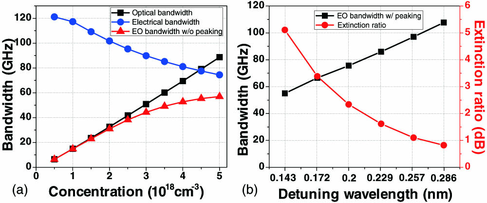
    Fig. 1. (a) Simulated optical bandwidth, electrical bandwidth, and EO bandwidth of the MRM with different doping concentrations, respectively. (b) Simulated EO bandwidth with optical peaking and extinction ratio (ER) of the MRM with different detuning wavelengths. The ER is simulated with the 3Vpp and 4.5 V reversed-bias voltage.
    (a) Schematic for the high-performance MRM. (b) PN junction in the MRM indicated by dashed square in (a). (c) Microscope picture of the proposed MRM.
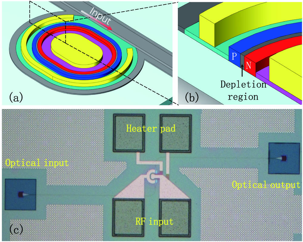
    Fig. 2. (a) Schematic for the high-performance MRM. (b) PN junction in the MRM indicated by dashed square in (a). (c) Microscope picture of the proposed MRM.
    (a) Normalized optical transmission by varying the reversed-bias voltages. (b) Extracted insertion loss (IL) and ER with different working wavelength with driving voltage of 3Vpp.
    Fig. 3. (a) Normalized optical transmission by varying the reversed-bias voltages. (b) Extracted insertion loss (IL) and ER with different working wavelength with driving voltage of 3Vpp.
    Measured EO response with 2 V reversed-bias voltage. The EO bandwidths of 110, 91, 79, 65, and 52 GHz are measured with the detuning wavelength Δλ of 0.326, 0.269, 0.24, 0.183, and 0.115 nm, respectively.
    Fig. 4. Measured EO response with 2 V reversed-bias voltage. The EO bandwidths of 110, 91, 79, 65, and 52 GHz are measured with the detuning wavelength Δλ of 0.326, 0.269, 0.24, 0.183, and 0.115 nm, respectively.
    Experimental setup of the transmission based on the MRM. Tx, transmitter; Rx, receiver; DSO, digital storage oscilloscope; AWG, arbitrary wave generator; PC, polarization controller; PD, photodetector; EA, electrical amplifier; VOA, variable optical attenuator; SSMF, standard single-mode fiber; EQ, equalization; NN, neural network; NLC, nonlinear compensation.
    Fig. 5. Experimental setup of the transmission based on the MRM. Tx, transmitter; Rx, receiver; DSO, digital storage oscilloscope; AWG, arbitrary wave generator; PC, polarization controller; PD, photodetector; EA, electrical amplifier; VOA, variable optical attenuator; SSMF, standard single-mode fiber; EQ, equalization; NN, neural network; NLC, nonlinear compensation.
    Measured BER for 110, 115, and 120 Gb/s NRZ at different received optical power. Inset: eye diagram after equalization of 120 Gb/s NRZ signal.
    Fig. 6. Measured BER for 110, 115, and 120 Gb/s NRZ at different received optical power. Inset: eye diagram after equalization of 120 Gb/s NRZ signal.
    (a) Measured BER for BtB and after 2 km SSMF transmission with different data rates for PAM-4 signal of the MRM. Inset: diagram of 220 Gb/s PAM-4 signal. (b) Measured BER for 200 Gb/s PAM-4 signal at different received optical powers. Inset: diagram of 200 Gb/s PAM-4 signal.
    Fig. 7. (a) Measured BER for BtB and after 2 km SSMF transmission with different data rates for PAM-4 signal of the MRM. Inset: diagram of 220 Gb/s PAM-4 signal. (b) Measured BER for 200 Gb/s PAM-4 signal at different received optical powers. Inset: diagram of 200 Gb/s PAM-4 signal.
    (a) Measured BER for BtB and after 2 km SSMF transmission with different data rates for PAM-8 signal of the MRM. Inset: diagram of 240 Gb/s PAM-8. (b) Calculated BER for 180 Gb/s PAM-8 signal at different received optical powers. Inset: diagram of 180 Gb/s PAM-8.
    Fig. 8. (a) Measured BER for BtB and after 2 km SSMF transmission with different data rates for PAM-8 signal of the MRM. Inset: diagram of 240 Gb/s PAM-8. (b) Calculated BER for 180 Gb/s PAM-8 signal at different received optical powers. Inset: diagram of 180 Gb/s PAM-8.
    PlatformTypeEO Bandwidth (GHz)Vπ·L(V·cm)Vpp(V)Footprint (mm)Data Rate (Gb/s)FormatDSP
    III–V/SiC [9]DMLa108N.A.1.750.05256 (HD-FEC)PAM4Off-line, 101-tap FFE & 61-tap Volterra
    LNOI [17]MZI>702.7/b9128 (HD-FEC)PAM431-tap FFE
    SOI [3]MZI601.452112PAM4W/o
    SOI [5]MZI471.352.32.5225 (SD-FEC)PAM8Off-line, 81-tap FFE& Volterra
    SOI [23]MRR770.531.60.006c192PAM4Off-line, 5-tap FFE & TDECQ
    POH [13]MZI700.00630.0172 (HD-FEC)OOK9-tap delay filter
    SOH [11]MZI681.441.38200 (HD-FEC)PAM4Off-line, Nyquist pulse shaping
    SOI (this work)MRR >600.830.008c240 (SD-FEC)PAM8Off-line, NN & MLSE
    Table 1. Performance Comparison of High-Speed EO Modulators
    Yuguang Zhang, Hongguang Zhang, Junwen Zhang, Jia Liu, Lei Wang, Daigao Chen, Nan Chi, Xi Xiao, Shaohua Yu. 240 Gb/s optical transmission based on an ultrafast silicon microring modulator[J]. Photonics Research, 2022, 10(4): 1127
    Download Citation