
Yuguang Zhang, Hongguang Zhang, Junwen Zhang, Jia Liu, Lei Wang, Daigao Chen, Nan Chi, Xi Xiao, Shaohua Yu, "240 Gb/s optical transmission based on an ultrafast silicon microring modulator," Photonics Res. 10, 1127 (2022)
- Photonics Research
- Vol. 10, Issue 4, 1127 (2022)
Abstract
1. INTRODUCTION
The fast development of artificial intelligence (AI), 5G applications, cloud computation, and internet of things (IoT) requires high-speed optical modules in optical interconnections. As one of the building blocks of optical communication, optical modulators [1] with high bandwidth, low loss, and low driving voltage are desired. Mach–Zehnder modulators (MZMs), including silicon modulators [2–5], indium phosphide (InP) modulators and lasers [6–9], silicon organic hybrid (SOH) modulators [10,11], plasmonic-organic hybrid (POH) modulators [12,13], and lithium niobate on insulator (LNOI) modulators [14–17], are intensively investigated. Among these technologies, silicon photonics technology is considered to be one of the best approaches, due to its high integration, low fabrication cost, and compatibility with mature CMOS process [1,18]. Although MZMs have the advantage of large bandwidth, there are drawbacks, including high optical loss, large footprint, high driving voltage, and high-power consumption. Compared with the MZMs, microring modulators (MRMs) [19–23] can overcome the disadvantages aforementioned.
Over recent years, MRMs have attracted increasing interest, and modulation over 100 Gb/s [24,25] PAM4 has been experimentally demonstrated. Optical peaking [26,27] is researched to enlarge the EO bandwidth. Through this approach, a 50 GHz EO bandwidth MRM [28] supporting 128 Gb/s PAM4 modulation is achieved. However, achieving a modulation data rate higher than 200 Gb/s is still a big challenge for MRM.
An ultrafast MRM is experimentally demonstrated. We achieved the large bandwidth of 110 GHz through optimizing the doping concentration and optical peaking of the proposed MRM. The
Sign up for Photonics Research TOC. Get the latest issue of Photonics Research delivered right to you!Sign up now
2. DESIGN AND FABRICATION
Both the photon lifetime limited optical bandwidth and the resistance-capacitance constant limited electrical bandwidth determine the EO bandwidth of the MRMs, as described by [29,30]
The photon lifetime of the MRM is defined by
To investigate the relationship between the performance of the MRMs and the doping concentration, we simulated the optical bandwidth, electrical bandwidth, and EO bandwidth with different doping concentrations. Figure 1(a) presents the simulated results. The carrier distribution of the PN junction is simulated by a Lumerical device to obtain the series resistance and PN junction capacitance. Then, the simulated carrier distribution is sent to mode solutions to calculate the optical loss and effective index at different reversed-bias voltages. Lumerical interconnect is used to simulate the optical transmission spectra of the MRM, and the
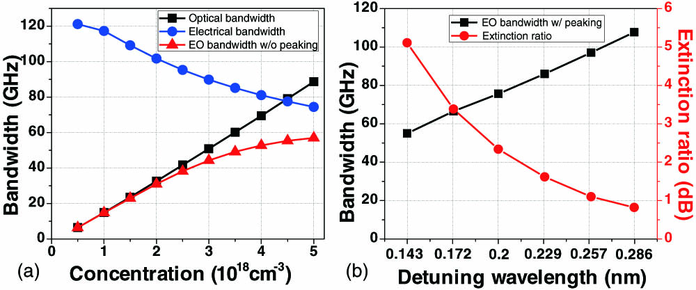
Figure 1.(a) Simulated optical bandwidth, electrical bandwidth, and EO bandwidth of the MRM with different doping concentrations, respectively. (b) Simulated EO bandwidth with optical peaking and extinction ratio (ER) of the MRM with different detuning wavelengths. The ER is simulated with the 3
The electrical bandwidth of the MRMs will decrease with heavier doping concentration, due to the larger junction capacitance [32]. The optical bandwidth will increase, along with the doping concentration. The overall EO bandwidth of the MRMs is calculated based on Eq. (1). The increase of the EO bandwidth for the MRM becomes slower for doping concentration larger than
We designed the proposed high-speed MRM based on the 220 nm SOI platform. The schematic of the proposed MRM is presented in Fig. 2(a). The radius of the MRM is designed to be 8 μm. The waveguide width of 420 nm is designed with the slab thickness of 70 nm
![]()
Figure 2.(a) Schematic for the high-performance MRM. (b) PN junction in the MRM indicated by dashed square in (a). (c) Microscope picture of the proposed MRM.
The proposed MRM is fabricated in a commercial 8 in. 130 nm CMOS foundry with three metal layers and one TiN heater layer. Figure 2(c) is the microscope picture of the fabricated MRM. The ground-signal (G-S) electrode with the pitch of 150 μm is designed for implementing the RF signal. The CW light from the optical fiber is coupled into the proposed MRM through the grating couplers. The resonant wavelength of the MRM will be affected by fabrication errors or temperature variations and deviate from the desired value. Thus, we implemented an integrated TiN heater above the MRM to control the resonant wavelength.
The normalized optical transmission by varying the reversed-bias voltage is shown in Fig. 3(a). The
![]()
Figure 3.(a) Normalized optical transmission by varying the reversed-bias voltages. (b) Extracted insertion loss (IL) and ER with different working wavelength with driving voltage of
With a Keysight’s 110 GHz light wave component analyzer (LCA, N4372E), we characterized the EO response for the high bandwidth MRM. In order to obtain an accurate EO response, influences caused by cables and probe are de-embedded. The PN junction capacitance
![]()
Figure 4.Measured EO response with 2 V reversed-bias voltage. The EO bandwidths of 110, 91, 79, 65, and 52 GHz are measured with the detuning wavelength
3. HIGH-SPEED CHARACTERIZATION
NRZ, PAM-4, and PAM-8 signal modulations of our proposed MRM are carried out through the measurement setup shown in Fig. 5. The output power of the tunable laser is 15 dBm. We adjusted the output light to TE mode with a polarization controller (PC) and coupled the TE mode to the MRM through the grating couplers. To simplify the measurement, we adjusted the output wavelength of the tunable laser instead of tuning the TiN heater. The RF signal is generated by a 120 GS/s arbitrary wave generator (AWG). An SHF driver (S807 C, bandwidth of 55 GHz) is used with the output voltage swing of 3Vpp. After amplification, the RF signal is sent to the MRM with a high bandwidth G-S probe. To reduce the RF reflection, a 50 Ω termination contacts the MRM through an S-G probe. Meanwhile, 4.5 V reversed-bias voltage for the PN junction is provided by a DC power supplier and a bias tee. The output optical signal power from the MRM is more than 2.5 dBm and is adjusted with a variable optical attenuator (VOA). The total insertion loss is about 12.5 dB, including 8 dB for two grating couplers, 1.5 dB for optical fiber transmission loss (polarization controller, fibers, and connectors), and 3 dB for bias loss, corresponding to about 0.148 nm wavelength detuning. The bandwidth at this detuning point is estimated to be larger than 60 GHz. A 50 GHz commercial photodetector (PD) is used to receive the optical signal. Since high-bandwidth trans-impedance amplifier (TIA) is not available, an electrical amplifier is used to enhance the received signal. We captured the amplified electrical signal by a 256 GS/s real-time digital storage oscilloscope (DSO) and calculated the BER through off-line digital signal processing (DSP).
![]()
Figure 5.Experimental setup of the transmission based on the MRM. Tx, transmitter; Rx, receiver; DSO, digital storage oscilloscope; AWG, arbitrary wave generator; PC, polarization controller; PD, photodetector; EA, electrical amplifier; VOA, variable optical attenuator; SSMF, standard single-mode fiber; EQ, equalization; NN, neural network; NLC, nonlinear compensation.
In the high-speed transmission measurement of the proposed MRM, we applied joint off-line signal processing in the Tx and Rx side to improve the overall performance. At the Tx side, the pre-equalization is employed to compensate for the linear impairments caused by limited component bandwidth [34]. At the Rx side, the neural network (NN)-based nonlinear compensation (NLC) [35] at 1 sample per symbol (sps) was used to mitigate the nonlinear impairments for PAM signals, followed by the maximum likelihood sequence equalization (MLSE) to handle the residual linear impairments [36].
Figure 6 shows the measured BER with different data rates for NRZ signal transmission based on the MRM. The BtB BER of 120 Gb/s NRZ is calculated to be
![]()
Figure 6.Measured BER for 110, 115, and 120 Gb/s NRZ at different received optical power. Inset: eye diagram after equalization of 120 Gb/s NRZ signal.
The PAM-4 signal transmission based on the proposed MRM is measured. Figure 7(a) displays the calculated BER of BtB and after 2 km transmission with different data rates. The BER of 220 Gb/s PAM-4 is calculated to be
![]()
Figure 7.(a) Measured BER for BtB and after 2 km SSMF transmission with different data rates for PAM-4 signal of the MRM. Inset: diagram of 220 Gb/s PAM-4 signal. (b) Measured BER for 200 Gb/s PAM-4 signal at different received optical powers. Inset: diagram of 200 Gb/s PAM-4 signal.
For the purpose of further increasing the modulation data rate, we test the performance of PAM-8 signal transmission based on the proposed MRM with the same setup. The calculated BER for PAM-8 signal with a different baud rate is shown in Fig. 8(a). The highest data rate of 240 Gb/s PAM-8 is achieved with the BER of
![]()
Figure 8.(a) Measured BER for BtB and after 2 km SSMF transmission with different data rates for PAM-8 signal of the MRM. Inset: diagram of 240 Gb/s PAM-8. (b) Calculated BER for 180 Gb/s PAM-8 signal at different received optical powers. Inset: diagram of 180 Gb/s PAM-8.
The performance of our MRM is compared with the prior state-of-the art demonstrations, consisting of III–V on a SiC directly modulated laser (DML) [9], LNOI modulator [17], silicon Mach–Zehnder modulator [3,5], silicon microring modulator [23], POH modulator [13], and SOH modulator [11], as shown in Table 1. Compared with Mach–Zehnder modulators, the insertion loss in MRMs is predominantly determined by the wavelength detuning point while having negligible correlation with the waveguide loss. This is important for next-generation optical interconnects, since the optical power budget is becoming increasingly critical. The present device experimentally demonstrated 240 Gb/s PAM8 modulation, which is the highest modulation speed among all the modulators in silicon photonics. The proposed MRM also features the advantages of large bandwidth and small footprint, which are comparable with the best demonstrated performances of the prior modulators. All these characters make the proposed MRM appeal for the applications in high-speed data-center interconnect (DCI).
Performance Comparison of High-Speed EO Modulators
| Platform | Type | EO Bandwidth | Footprint | Data Rate | Format | DSP | ||
|---|---|---|---|---|---|---|---|---|
| III–V/SiC [ | DML | 108 | N.A. | 1.75 | 0.05 | 256 (HD-FEC) | PAM4 | Off-line, 101-tap FFE & 61-tap Volterra |
| LNOI [ | MZI | 2.7 | / | 9 | 128 (HD-FEC) | PAM4 | 31-tap FFE | |
| SOI [ | MZI | 1.4 | 5 | 2 | 112 | PAM4 | W/o | |
| SOI [ | MZI | 47 | 1.35 | 2.3 | 2.5 | 225 (SD-FEC) | PAM8 | Off-line, 81-tap FFE& Volterra |
| SOI [ | MRR | 77 | 0.53 | 1.6 | 0.006 | 192 | PAM4 | Off-line, 5-tap FFE & TDECQ |
| POH [ | MZI | 70 | 0.006 | 3 | 0.01 | 72 (HD-FEC) | OOK | 9-tap delay filter |
| SOH [ | MZI | 68 | 1.44 | 1.3 | 8 | 200 (HD-FEC) | PAM4 | Off-line, Nyquist pulse shaping |
| SOI (this work) | MRR | | 0.8 | 3 | 0.008 | 240 (SD-FEC) | PAM8 | Off-line, NN & MLSE |
Directly modulated laser (DML).
Not provided.
Radius of the MRR.
4. DISCUSSION
The performances of the proposed MRM are partially hindered by the devices used in our experiment. The system bandwidth is limited by the 50 GHz commercial PD. Since a high-bandwidth transimpedance amplifier (TIA) is not available, the electrical amplifier is necessary to enhance the received signal, which will increase the noise and the measured BER. Therefore, we can improve the measured results of the MRM by three ways: (i) replacing the PD with another possessing larger bandwidth; (ii) using the edge couplers with higher coupling efficiency to decrease the optical loss; (iii) adding a praseodymium-doped fiber amplifier to amplify the output optical signal. In these ways, the system bandwidth of the experimental setup can be improved and the electrical amplifier can be removed. As a result, the measured BER for different modulation formats, i.e., NRZ, PAM-4, and PAM-8 signals in our work, will decrease.
Considering the high performances, we can integrate the proposed MRM to achieve terabit-per-second optical transmission by wavelength division multiplexing (WDM) [37] in the future. The proposed MRM can also be used to realize high-speed in-phase/quadrature modulation [38]. Recently, heterogeneous III–V-on-silicon photonic integration [39] is developing rapidly. We believe that the performance of the MRM can be further improved by heterogeneous III–V-on-silicon photonic integration [39].
For off-line signal processing complexity, in our experimental test, the NN-based nonlinear compensation with a multilayer perceptron (MLP) algorithm is used to compensate for residual linear and nonlinear distortions in the signal. The number of input nodes of the MLP is set to nine; the number of the first hidden layer should be 512. The current results are evaluated by using off-line DSP. As reported in Ref. [40], the NN-based equalization can be realized in real-time FPGA. We will study the complexity and realization in real-time processing in future work, for example, using FPGA [40].
5. CONCLUSION
The ultrahigh-speed MRM is proposed and developed. The doping concentration is optimized to enlarge the EO bandwidth and ER. The optical peaking is utilized to further extend the EO bandwidth. The measured
Acknowledgment
Acknowledgment. The authors thank Keysight Technologies for the support on device tests and measurements. Dr. Xi Xiao thanks Dr. Di Liang, Dr. Min Sun, and Dr. Bo Zhang for insightful discussions.
References
[1] G. T. Reed, G. Mashanovich, F. Y. Gardes, D. J. Thomson. Silicon optical modulators. Nat. Photonics, 4, 518-526(2010).
[2] M. R. Watts, W. A. Zortman, D. C. Trotter, R. W. Young, A. L. Lentine. Low-voltage, compact, depletion-mode, silicon Mach–Zehnder modulator. IEEE J. Sel. Top. Quantum Electron., 16, 159-164(2010).
[3] M. Li, L. Wang, X. Li, X. Xiao, S. Yu. Silicon intensity Mach–Zehnder modulator for single lane 100 Gb/s applications. Photon. Res., 6, 109-116(2018).
[4] H. Zhang, M. Li, Y. Zhang, D. Zhang, Q. Liao, J. He, S. Hu, B. Zhang, L. Wang, X. Xiao, N. Qi, S. Yu. 800 Gb/s transmission over 1 km single-mode fiber using a four-channel silicon photonic transmitter. Photon. Res., 8, 1776-1782(2020).
[5] M. S. Alam, X. Li, M. Jacques, Z. Xing, A. Samani, E. El-Fiky, P. Koh, D. V. Plant. Net 220 Gbps/
[6] J.-H. Han, F. Boeuf, J. Fujikata, S. Takahashi, S. Takagi, M. Takenaka. Efficient low-loss InGaAsP/Si hybrid MOS optical modulator. Nat. Photonics, 11, 486-490(2017).
[7] Y. Ogiso, J. Ozaki, Y. Ueda, H. Wakita, M. Nagatani, H. Yamazaki, M. Nakamura, T. Kobayashi, S. Kanazawa, T. Fujii, Y. Hashizume, H. Tanobe, N. Nunoya, M. Ida, Y. Miyamoto, M. Ishikawa. Ultra-high bandwidth InP IQ modulator for beyond 100-GBd transmission. Optical Fiber Communications Conference and Exhibition (OFC), M2F.2(2019).
[8] Y. Ogiso, J. Ozaki, Y. Ueda, N. Kashio, N. Kikuchi, E. Yamada, H. Tanobe, S. Kanazawa, H. Yamazaki, Y. Ohiso, T. Fujii, M. Kohtoku. Over 67 GHz bandwidth and 1.5 V
[9] S. Yamaoka, N. P. Diamantopoulos, H. Nishi, R. Nakao, T. Fujii, K. Takeda, T. Hiraki, T. Tsurugaya, S. Kanazawa, H. Tanobe, T. Kakitsuka, T. Tsuchizawa, F. Koyama, S. Matsuo. Directly modulated membrane lasers with 108 GHz bandwidth on a high-thermal-conductivity silicon carbide substrate. Nat. Photonics, 15, 28-35(2021).
[10] L. Alloatti, R. Palmer, S. Diebold, K. P. Pahl, B. Chen, R. Dinu, M. Fournier, J.-M. Fedeli, T. Zwick, W. Freude, C. Koos, J. Leuthold. 100 GHz silicon–organic hybrid modulator. Light Sci. Appl., 3, e173(2014).
[11] G.-W. Lu, J. Hong, F. Qiu, A. M. Spring, T. Kashino, J. Oshima, M. Ozawa, H. Nawata, S. Yokoyama. High-temperature-resistant silicon-polymer hybrid modulator operating at up to 200 Gbit s−1 for energy-efficient datacentres and harsh-environment applications. Nat. Commun., 11, 4224(2020).
[12] W. Heni, Y. Fedoryshyn, B. Baeuerle, A. Josten, C. B. Hoessbacher, A. Messner, C. Haffner, T. Watanabe, Y. Salamin, U. Koch, D. L. Elder, L. R. Dalton, J. Leuthold. Plasmonic IQ modulators with attojoule per bit electrical energy consumption. Nat. Commun., 10, 1694(2019).
[13] C. Haffner, W. Heni, Y. Fedoryshyn, J. Niegemann, A. Melikyan, D. L. Elder, B. Baeuerle, Y. Salamin, A. Josten, U. Koch, C. Hoessbacher, F. Ducry, L. Juchli, A. Emboras, D. Hillerkuss, M. Kohl, L. R. Dalton, C. Hafner, J. Leuthold. All-plasmonic Mach–Zehnder modulator enabling optical high-speed communication at the microscale. Nat. Photonics, 9, 525-528(2015).
[14] C. Wang, M. Zhang, X. Chen, M. Bertrand, A. Shams-Ansari, S. Chandrasekhar, P. Winzer, M. Lončar. Integrated lithium niobate electro-optic modulators operating at CMOS-compatible voltages. Nature, 562, 101-104(2018).
[15] Y. Zhang, M. Xu, H. Zhang, M. Li, J. Jian, M. He, L. Chen, L. Wang, X. Cai, X. Xiao, S. Yu. 220 Gb/s optical PAM-4 modulation based on lithium niobate on insulator modulator. 45th European Conference on Optical Communication (ECOC), PD2.6(2019).
[16] M. Xu, M. He, H. Zhang, J. Jian, Y. Pan, X. Liu, L. Chen, X. Meng, H. Chen, Z. Li, X. Xiao, S. Yu, S. Yu, X. Cai. High-performance coherent optical modulators based on thin-film lithium niobate platform. Nat. Commun., 11, 3911(2020).
[17] S. Sun, M. He, M. Xu, S. Gao, Z. Chen, X. Zhang, Z. Ruan, X. Wu, L. Zhou, L. Liu, C. Lu, C. Guo, L. Liu, S. Yu, X. Cai. Bias-drift-free Mach–Zehnder modulators based on a heterogeneous silicon and lithium niobate platform. Photon. Res., 8, 1958-1963(2020).
[18] L. Liu, R. Kumar, K. Huybrechts, T. Spuesens, G. Roelkens, E.-J. Geluk, T. Vries, P. Regreny, D. Van Thourhout, R. Baets, G. Morthier. An ultra-small, low-power, all-optical flip-flop memory on a silicon chip. Nat. Photonics, 4, 182-187(2010).
[19] Q. Xu, B. Schmidt, S. Pradhan, M. Lipson. Micrometre-scale silicon electro-optic modulator. Nature, 435, 325-327(2005).
[20] J. Rhim, Y. Ban, B.-M. Yu, J.-M. Lee, W.-Y. Choi. Verilog-A behavioral model for resonance- modulated silicon micro-ring modulator. Opt. Express, 23, 8762-8772(2015).
[21] X. Xiao, H. Xu, X. Li, Y. Hu, K. Xiong, Z. Li, T. Chu, Y. Yu, J. Yu. 25 Gb/s silicon microring modulator based on misalignment-tolerant interleaved PN junctions. Opt. Express, 20, 2507-2515(2012).
[22] X. Xiao, X. Li, H. Xu, Y. Hu, K. Xiong, Z. Li, T. Chu, J. Yu, Y. Yu. 44-Gb/s silicon microring modulators based on zigzag PN junctions. IEEE Photon. Technol. Lett., 24, 1712-1714(2012).
[23] M. Sakib, P. Liao, C. Ma, R. Kumar, D. Huang, G. Su, X. Wu, S. Fathololoumi, H. Rong. A high-speed micro-ring modulator for next generation energy-efficient optical networks beyond 100 Gbaud. Conference on Lasers and Electro-Optics (CLEO), SF1C.3(2021).
[24] Y. Ban, J. Verbist, M. Vanhoecke, J. Bauwelinck, P. Verheyen, S. Lardenois, M. Pantouvaki, J. Van Campenhout. Low-voltage 60 Gb/s NRZ and 100 Gb/s PAM-4 O-band silicon ring modulator. IEEE Optical Interconnects Conference(2019).
[25] Y. Tong, Z. Hu, X. Wu, S. Liu, L. Chang, A. Netherton, C.-K. Chan, J. E. Bowers, H. K. Tsang. An experimental demonstration of 160-Gb/s PAM-4 using a silicon micro-ring modulator. IEEE Photon. Technol. Lett., 32, 125-128(2019).
[26] J. Muller, F. Merget, S. S. Azadeh, J. Hauck, S. R. Garcıa, B. Shen, J. Witzens. Optical peaking enhancement in high-speed ring modulators. Sci. Rep., 4, 6310(2014).
[27] L. Zhang, Y. Li, J.-Y. Yang, M. Song, R. G. Beausoleil, A. E. Willner. Silicon-based microring resonator modulators for intensity modulation. IEEE J. Sel. Top. Quantum Electron., 16, 149-158(2010).
[28] J. Sun, R. Kumar, M. Sakib, J. B. Driscoll, H. Jayatilleka, H. Rong. A 128 Gb/s PAM-4 silicon microring modulator with integrated thermo-optic resonance tuning. J. Lightwave Technol., 37, 110-115(2019).
[29] P. Dong, S. Liao, D. Feng, H. Liang, D. Zheng, R. Shafiiha, C.-C. Kung, W. Qian, G. Li, X. Zheng, A. V. Krishnamoorthy, M. Asghari. Low
[30] G. Li, A. V. Krishnamoorthy, I. Shubin, J. Yao, Y. Luo, H. Thacker, X. Zheng, K. Raj, J. E. Cunningham. Ring resonator modulators in silicon for interchip photonic links. IEEE J. Sel. Top. Quantum Electron., 19, 95-113(2013).
[31] M. Shin, Y. Ban, B. M. Yu, M. H. Kim, J. Rhim, L. Zimmermann, W. Y. Choi. A linear equivalent circuit model for depletion-type silicon microring modulators. IEEE Trans. Electron Devices, 64, 1140-1145(2017).
[32] M. Pantouvaki, H. Yu, M. Rakowski, P. Christie, P. Verheyen, G. Lepage, N. V. Hoovels, P. Absil, J. V. Campenhout. Comparison of silicon ring modulators with interdigitated and lateral PN junctions. IEEE J. Sel. Top. Quantum Electron., 19, 7900308(2013).
[33] Y. Zhang, H. Zhang, M. Li, P. Feng, L. Wang, X. Xiao, S. Yu. 200 Gb/s optical PAM4 modulation based on silicon microring modulator. European Conference on Optical Communications (ECOC), Th3A-1(2020).
[34] J. Zhang, J. Yu, N. Chi, H.-C. Chien. Time-domain digital pre-equalization for band-limited signals based on receiver-side adaptive equalizers. Opt. Express, 22, 20515-20529(2014).
[35] N. Chi, Y. Zhao, M. Shi, P. Zou, X. Lu. Gaussian kernel-aided deep neural network equalizer utilized in underwater PAM8 visible light communication system. Opt. Express, 26, 26700-26712(2018).
[36] Z. Jia, Y. Cai, H.-C. Chien, J. Yu. Performance comparison of spectrum-narrowing equalizations with maximum likelihood sequence estimation and soft-decision output. Opt. Express, 22, 6047-6059(2014).
[37] Q. Xu, B. Schmidt, J. Shakya, M. Lipson. Cascaded silicon micro-ring modulators for WDM optical interconnection. Opt. Express, 14, 9431-9436(2006).
[38] P. Dong, C. Xie, L. Chen, N. K. Fontaine, Y.-K. Chen. Experimental demonstration of microring quadrature phase-shift keying modulators. Opt. Lett., 37, 1178-1180(2012).
[39] D. Liang, J. E. Bowers. Recent progress in heterogeneous III–V-on-silicon photonic integration. Light Adv. Manuf., 2, 59-83(2021).
[40] N. Kaneda, Z. Zhu, C. Chuang, A. Mahadevan, B. Farah, K. Bergman, D. Van Veen, V. Houtsma. FPGA implementation of deep neural network based equalizers for high-speed PON. Optical Fiber Communications Conference and Exhibition (OFC), T4D.2(2020).


Set citation alerts for the article
Please enter your email address

© Copyright 2018-2021 | Chinese Laser Press. All Rights Reserved 沪ICP备15018463号-20