• Photonics Research
  • Vol. 4, Issue 5, 0173 (2016)
Ahmad A. Darweesh1, Stephen J. Bauman1, and Joseph B. Herzog1、2、*
Author Affiliations
  • 1Microelectronics-Photonics Graduate Program, University of Arkansas, Fayetteville, Arkansas 72701, USA
  • 2Department of Physics, University of Arkansas, Fayetteville, Arkansas 72701, USA
  • show less
    DOI: 10.1364/prj.4.000173 Cite this Article Set citation alerts
    Ahmad A. Darweesh, Stephen J. Bauman, Joseph B. Herzog. Improved optical enhancement using double-width plasmonic gratings with nanogaps[J]. Photonics Research, 2016, 4(5): 0173 Copy Citation Text show less
    Sketch of the double-width plasmonic grating design with nanogap spacing. The nanostructure height, t, period, P, the short width, wS, the long width, wL, and the nanogap width, g, are labeled.
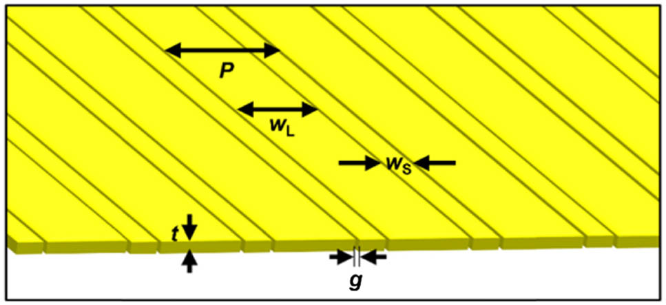
    Fig. 1. Sketch of the double-width plasmonic grating design with nanogap spacing. The nanostructure height, t, period, P, the short width, wS, the long width, wL, and the nanogap width, g, are labeled.
    (a) Depiction of cross-sectional simulation space that contains a single period of the dual-width plasmonic Au grating. The PMLs as well as the structure and gap widths (wS, wL, and g, respectively) are labeled. The incident light direction is k, and E0 is the direction of polarization. Periodic boundary conditions were applied in both horizontal directions. (b) Optical enhancement distribution simulation results when wS=60 nm, wL=360 nm, and λ0=700 nm. The box over the gap is the region of interest and does not alter any material properties of the structure.
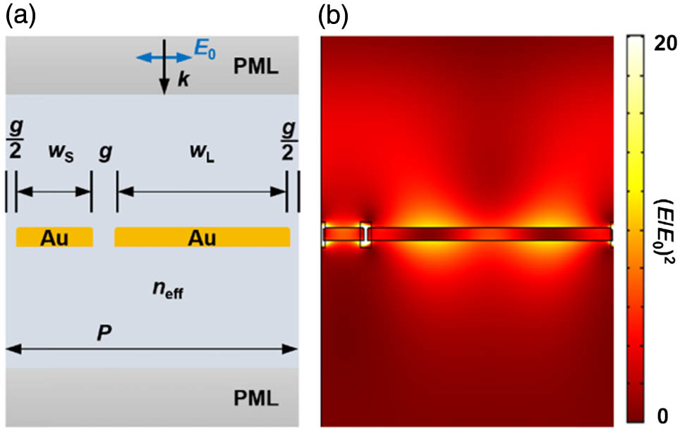
    Fig. 2. (a) Depiction of cross-sectional simulation space that contains a single period of the dual-width plasmonic Au grating. The PMLs as well as the structure and gap widths (wS, wL, and g, respectively) are labeled. The incident light direction is k, and E0 is the direction of polarization. Periodic boundary conditions were applied in both horizontal directions. (b) Optical enhancement distribution simulation results when wS=60  nm, wL=360  nm, and λ0=700  nm. The box over the gap is the region of interest and does not alter any material properties of the structure.
    (a)–(c) Optical enhancement, Σ(E/E0)2, in the gap for double-width plasmonic grating geometries as a function of wS and wL for three incident wavelengths (λ0=600, 700, and 800 nm); wS and wL range from 10 to 250 nm in 10 nm steps. (d) w values at the peak wavelengths for each of the three resonant periods in the width range. (e) Enhancement as a function of gold width (wS=wL) with the range extended from 10 to 1000 nm for the same wavelengths and step size as in (a)–(c).
    Fig. 3. (a)–(c) Optical enhancement, Σ(E/E0)2, in the gap for double-width plasmonic grating geometries as a function of wS and wL for three incident wavelengths (λ0=600, 700, and 800 nm); wS and wL range from 10 to 250 nm in 10 nm steps. (d) w values at the peak wavelengths for each of the three resonant periods in the width range. (e) Enhancement as a function of gold width (wS=wL) with the range extended from 10 to 1000 nm for the same wavelengths and step size as in (a)–(c).
    (a) Optical enhancement for combinations of wS and wL from 10 to 1000 nm with λ0=700 nm. The positively sloped diagonal corresponds to wS=wL. Negatively sloped, constant-period diagonal lines correspond to the patterns of local and absolute enhancement maxima. Width combinations A and i–iii are points of interest. (b) Depiction of the geometry showing P and x=wS+g. (c) Plot of optical enhancement versus gap position, x, along the black diagonal line, from A to iii in (a), where P1=430 nm. (d) Plot of period width versus resonance number, corresponding to the periods in (a).
    Fig. 4. (a) Optical enhancement for combinations of wS and wL from 10 to 1000 nm with λ0=700  nm. The positively sloped diagonal corresponds to wS=wL. Negatively sloped, constant-period diagonal lines correspond to the patterns of local and absolute enhancement maxima. Width combinations A and i–iii are points of interest. (b) Depiction of the geometry showing P and x=wS+g. (c) Plot of optical enhancement versus gap position, x, along the black diagonal line, from A to iii in (a), where P1=430  nm. (d) Plot of period width versus resonance number, corresponding to the periods in (a).
    Simulation results of a nonperiodic model consisting of an isolated 5 μm Au slab with 15 nm height. Resulting charge distribution of the slab showing the resonant plasmon wavelength (λp) from a normal incident plane wave with the wavelength (λ0) set at 700 nm. λp was found to be 363 nm. One edge of the structure is visible at the far left.
    Fig. 5. Simulation results of a nonperiodic model consisting of an isolated 5 μm Au slab with 15 nm height. Resulting charge distribution of the slab showing the resonant plasmon wavelength (λp) from a normal incident plane wave with the wavelength (λ0) set at 700 nm. λp was found to be 363 nm. One edge of the structure is visible at the far left.
    Electric field and surface charge distribution results for P1=430 nm and width combinations labeled in Fig. 4(a). In (i), (ii), and (iii), wS are 60, 130, and 210 nm, and wL are 360, 290, and 210 nm, respectively. (a) Electric field distributions resulting from the different plasmons shown by (b) the charge distributions. Also see Visualization 1.
    Fig. 6. Electric field and surface charge distribution results for P1=430  nm and width combinations labeled in Fig. 4(a). In (i), (ii), and (iii), wS are 60, 130, and 210 nm, and wL are 360, 290, and 210 nm, respectively. (a) Electric field distributions resulting from the different plasmons shown by (b) the charge distributions. Also see Visualization 1.
    Simulation results for three different geometries at three different gap widths for constant period, P=430 nm, and Au width, wS=60 nm. Gap values of g=5, 20, and 50 nm were used and correspond to (i), (ii), and (iii), respectively. (a) Shows the three simulated geometries with similar widths. (b) Enhancement spectra for each situation. Gray wS curves represent enhancement near an isolated small stripe, red wL curves represent an isolated larger stripe, and blue dual curves were taken by including both gold structures.
    Fig. 7. Simulation results for three different geometries at three different gap widths for constant period, P=430  nm, and Au width, wS=60  nm. Gap values of g=5, 20, and 50 nm were used and correspond to (i), (ii), and (iii), respectively. (a) Shows the three simulated geometries with similar widths. (b) Enhancement spectra for each situation. Gray wS curves represent enhancement near an isolated small stripe, red wL curves represent an isolated larger stripe, and blue dual curves were taken by including both gold structures.
    Electric field distribution results of each gap width and geometry at the corresponding peak wavelengths. (a), (b), and (c) Correspond to Fig. 7(b) i, ii, and iii, respectively.
    Fig. 8. Electric field distribution results of each gap width and geometry at the corresponding peak wavelengths. (a), (b), and (c) Correspond to Fig. 7(b) i, ii, and iii, respectively.
    (a) Cross-sectional simulation space, which contains air, SiO2, and various double nanowire widths. (b) Plot of the optical enhancement versus wire width along the diagonal line in (c). (c) Optical enhancement of the structure when wS and wL were swept from 10 to 800 nm. Dashed diagonal line represents wS=wL, the standard plasmonic grating geometry.
    Fig. 9. (a) Cross-sectional simulation space, which contains air, SiO2, and various double nanowire widths. (b) Plot of the optical enhancement versus wire width along the diagonal line in (c). (c) Optical enhancement of the structure when wS and wL were swept from 10 to 800 nm. Dashed diagonal line represents wS=wL, the standard plasmonic grating geometry.
    Ahmad A. Darweesh, Stephen J. Bauman, Joseph B. Herzog. Improved optical enhancement using double-width plasmonic gratings with nanogaps[J]. Photonics Research, 2016, 4(5): 0173
    Download Citation