Ahmad A. Darweesh, Stephen J. Bauman, Joseph B. Herzog, "Improved optical enhancement using double-width plasmonic gratings with nanogaps," Photonics Res. 4, 0173 (2016)
Copy Citation Text
Plasmonic grating structures have been shown effective at increasing near-field optical enhancement. A doublewidth plasmonic grating design is introduced, where each period has two alternating metal widths separated by a nanogap. With this new design, analysis has shown that plasmonic resonances couple between each metal section, resulting in even greater optical enhancement compared with single-width gratings. The geometry that gives the greatest optical enhancement has been determined with a computational model. This work demonstrates that the increased enhancement is due to hybridized modes that couple between the two grating segments.
Plasmonic gratings, periodic arrays of metal structures separated by a dielectric, have been demonstrated to increase optical enhancement, benefitting a variety of photonics applications. Various slit, groove, and grating styles have been studied [1–3]. Circular gratings are used as plasmonic lenses for surface-enhanced nanoscale spectroscopy [4,5]. Experimental and theoretical work has confirmed that tunable grating structures enable the engineering of different desired spectral enhancements [6–10]. The number and period of grating rings, the material used, and the slit geometry are all controllable, thus demonstrating the flexibility of gratings as plasmonic tools for sensing applications [4]. Plasmonic gratings enhance light absorption, scattering, and optical detection [11–17]; they have been used in solar cell enhancement devices [18–22], biosensing [23–27], and fluorescence [28–31] applications. Slits are typically considered to be areas of a large metal slab where the metal has been removed [32,33]. Grooves tend to be depressed-height regions within a large metal area and often incorporate slanted walls [34–36]. Gratings can be periodic arrays of slits, grooves, or simply metallic wires, rods, or other structures. Here, arrays of long, isolated, metallic structures are referred to as standard or single plasmonic gratings. Reports on dual-step plasmonic gratings have shown stronger field intensities [2,14], but dual-width gratings still need investigation.
Beyond gratings, plasmonic devices of various geometries and configurations are also useful for enhancing optical applications. Bringing plasmonic structures close together until they are separated by nanoscale gaps has been shown to increase this light enhancement even further [37–40]. Moreover, gap widths approaching 10 nm or less display a nearly exponential increase in enhancement [41–49]. Thus, sub-10 nm gaps between plasmonically active devices hold promise as useful technology that utilizes these optical enhancement capabilities. These include, but are not limited to, enhanced photovoltaics [50–56], surface-enhanced Raman spectroscopy (SERS) and other spectroscopies [57–62], single molecule detection [62–65], and biosensors [66–72].
This work combines dual-width plasmonic gratings with sub-10 nm gaps to develop devices with increased optical enhancement factors. The devices can be fabricated via a recently developed lithography technique called nanomasking [73,74]. These structures differ from slits and grooves, as they are separate metallic structures, completely isolated from one another except via the surrounding media. The work shows that dual-width plasmonic gratings can more than double optical enhancement values over standard plasmonic gratings. Also reported is that the addition of a 5 nm gap spacing increases the optical field more than 40 times that of a similar structure with a 50 nm gap, highlighting the importance of sub-10 nm gaps.
Sign up for Photonics Research TOC. Get the latest issue of Photonics Research delivered right to you!Sign up now
2. DOUBLE-WIDTH GRATINGS
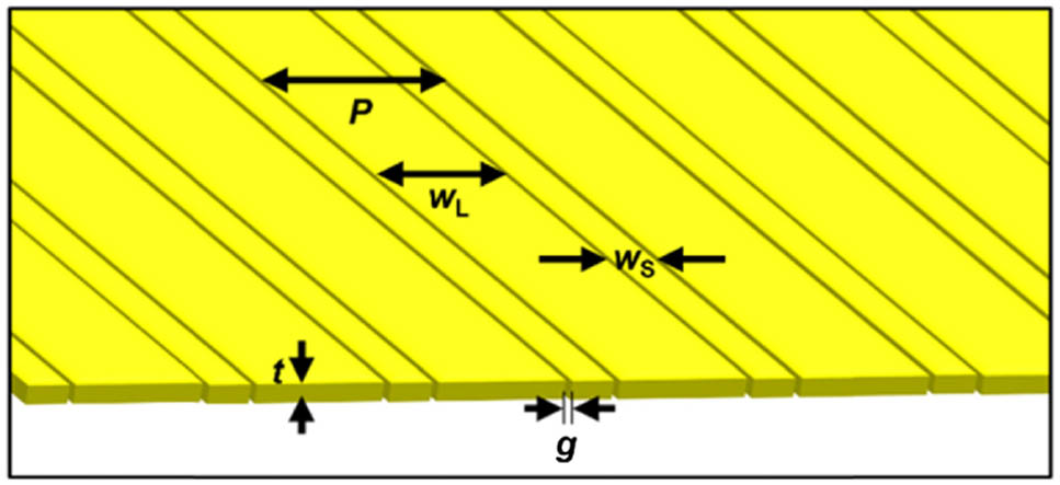
Double-width plasmonic gratings are defined here as gratings in which each period contains two metal nanostructure regions with unique widths. These are separated by a dielectric in addition to the separations between each period. This design is shown in Fig. 1. The period, , is equal to the sum of both gap widths, , plus the short and long widths of the gold regions, and , respectively. Thus, .
Figure 1.Sketch of the double-width plasmonic grating design with nanogap spacing. The nanostructure height, , period, , the short width, , the long width, , and the nanogap width, , are labeled.
The goal of this work was to determine the potential for utilizing the resulting structures in optical enhancement applications by optimizing the period size and Au structure width combination for this design. Thus, detailed simulations were performed for various geometries of these gratings.
3. METHODS
Finite element method (FEM) simulations were used to determine the optical enhancement produced by these dual-width plasmonic gratings (COMSOL 5.1). Figure 2(a) shows a cross-sectional view of one period of the grating structure used in the base simulation model. The schematic in this image is not to scale, so that the figure could be more clearly labeled. The variable model was made to consist of two Au nanostructures separated by a gap of width . Material properties for Au were taken from Johnson and Christy [75]. The model used an effective medium approximation for the surrounding medium, , to model a general case [76–78]. An additional model, which includes a substrate and demonstrates similar results, has been included (see Appendix A). The height of the gold stripes was fixed at 15 nm, and the widths ( and ) varied for each different calculation. Varying both widths made it possible to study the effects of a double-width plasmonic grating. The gap width was set at unless otherwise noted, and the top edges of the structures were beveled with a 5 nm radius of curvature to more accurately represent the experimentally realized geometry. A periodic condition was applied to the left and right edges of the model (in the center of the outer gaps), to make an infinitely repeating horizontal array with variable period, . Light of variable wavelength was simulated as being incident normal to the surface from the top of the space ( orientation) with the electric field () polarized in the direction of periodicity. Perfectly matched layers (PMLs) were applied to the top and bottom of the model to prevent scattered light from reflecting back into the space from these imaginary boundaries. Figure 2(b) displays an example of the resulting electric field distribution for and with . The black box containing the nanogap and inner metal edges, shown in Fig. 2(b), represents the region of interest where the optical signal is the greatest. The optical enhancement, , is the ratio of local light intensity to incident light intensity, the square of the local field divided by the incident field strength .
Figure 2.(a) Depiction of cross-sectional simulation space that contains a single period of the dual-width plasmonic Au grating. The PMLs as well as the structure and gap widths (, , and , respectively) are labeled. The incident light direction is , and is the direction of polarization. Periodic boundary conditions were applied in both horizontal directions. (b) Optical enhancement distribution simulation results when , , and . The box over the gap is the region of interest and does not alter any material properties of the structure.
To study the effects of a double-width grating, the two widths of the grating were varied, and the optical enhancement was calculated using the model in Fig. 2(a). First, ranges of both and from 10 to 250 nm were investigated for three different incident wavelengths: 600, 700, and 800 nm. The combined results of these calculations are shown in Fig. 3.
Figure 3.(a)–(c) Optical enhancement, , in the gap for double-width plasmonic grating geometries as a function of and for three incident wavelengths (, 700, and 800 nm); and range from 10 to 250 nm in 10 nm steps. (d) values at the peak wavelengths for each of the three resonant periods in the width range. (e) Enhancement as a function of gold width with the range extended from 10 to 1000 nm for the same wavelengths and step size as in (a)–(c).
Color maps of the enhancement at different width combinations are shown in Figs. 3(a)–3(c) for each incident wavelength. Each data point in the color maps is the optical enhancement near the gap for a specific geometry. The near-field gap enhancement, represented by , was calculated by summing the enhancement values within the region of interest, as depicted in Fig. 2(b). The positively sloped diagonal lines, , in these color maps correspond to the standard (single-width) grating condition. The data along these diagonals are plotted in Fig. 3(e) to illustrate the relationship between the optical enhancement and the structure widths for each wavelength shown in Fig. 3(a). The calculation was extended in Fig. 3(e) for the standard grating case, , in order to see the enhancement for widths from 10 to 1000 nm with a step size of 10 nm. This plot shows three clear resonant period lengths for each wavelength, labeled , , and . For Fig. 3(b), when , the period of the grating is , so the peaks in the enhancement can be dependent on the metal width and the period of the grating. The gold widths, , giving the peak enhancement were plotted as a function of for each resonant period, as shown in Fig. 3(d). This nearly linear relationship can help fabricate grating structures that are tuned to specific wavelength needs.
The off-diagonal regions in Fig. 3(a)–3(c) are the dual-width grating geometries where . These regions show some interesting enhancement areas; they are most visible for at widths greater than 200 nm. Therefore, this wavelength was investigated further for a double-width structure with an extended-width range.
Figure 4(a) shows optical enhancement for for an extended-width range up to 1000 nm as compared with Figs. 3(a)–3(c); note that the color bar was rescaled due to the fact that width combinations with greater enhancements were probed. As expected, these results are symmetric across the diagonal of . However, the interesting features of these results are that two of the dual-width grating geometries (off-diagonal) give the maximum optical enhancement. These maxima appear for symmetrical geometries and occur when and (and vice versa) with an optical enhancement value of . One of these symmetrical points is shown at the data point labeled (i) in Fig. 4(a). This enhancement is more than double the maximum value for the standard plasmonic grating (single-width) structure, which was close to for . It also should be noted that this dual-width maximum value occurs along the negatively sloped diagonal line of constant period where .
Figure 4.(a) Optical enhancement for combinations of and from 10 to 1000 nm with . The positively sloped diagonal corresponds to . Negatively sloped, constant-period diagonal lines correspond to the patterns of local and absolute enhancement maxima. Width combinations A and i–iii are points of interest. (b) Depiction of the geometry showing and . (c) Plot of optical enhancement versus gap position, , along the black diagonal line, from A to iii in (a), where . (d) Plot of period width versus resonance number, corresponding to the periods in (a).
A simplified depiction of the model geometry is shown in Fig. 4(b) for clarification. For the dual-width structure, because , the lines with negative slope are given by
Therefore, lines with slope of have a constant period, , because the gap width is set constant at for these calculations. Upon careful inspection of Fig. 4(a), one can see that these lines of constant period contain the regions of maximum optical enhancement, validating the importance of period in plasmonic grating structures. These periods are the resonant period lengths, , for plasmonic gratings with this particular geometry. These resonant period lengths, , increase linearly with . This relationship is plotted in Fig 4(d). This result confirms the significance of the period in plasmonic grating design [10,79–82] and that the optimal stripe width and period combinations for a given incident wavelength are related to the resonant plasmon wavelength, which was determined by the result in Fig. 5.
Figure 5.Simulation results of a nonperiodic model consisting of an isolated 5 μm Au slab with 15 nm height. Resulting charge distribution of the slab showing the resonant plasmon wavelength () from a normal incident plane wave with the wavelength set at 700 nm. was found to be 363 nm. One edge of the structure is visible at the far left.
The new finding here shows that a double-width plasmonic geometry gives the largest enhancement. This is highlighted in the plot in Fig. 4(c). These data were extracted from the line of constant period, , for width combinations along the black diagonal line [from point A to iii in Fig. 4(a)]. The enhancement was plotted versus the gap position, , which is shown in Fig. 4(b), and defined as . The ratio of the widths changes with , again showing that the maximum enhancement value, is for widths of and . A video of the effects of the gap position also is available in the supplemental material. Along the positively sloped diagonal, for the standard single-width grating , the greatest enhancement appears only at the periods with even multiples of . However, it is also important to note that, when , the period becomes because now the irreducible period only contains one metal stripe, not two as in the dual-width case.
Because the period plays a significant role in plasmonic grating structures, a nonperiodic model was used to simulate the effect of incident light irradiation on a much wider (5 μm), isolated, thin Au slab. This test was established to determine the resonant plasmon wavelength, , for the incident light wavelength used in Fig. 4, , and for a thickness, , of 15 nm. The surface plasmon charge distribution map, as calculated by the simulation, is shown in Fig. 5 near the edge of a thin Au slab. The charge map was used to determine the value of the resonant plasmonic wavelength for this structure, which was measured to be for a normally incident 700 nm plane wave. For the standard single-width grating, when , the enhancement in the gap is a minimum [see Fig. 3(e)]. Here, when the width of the Au structure matches the resonant plasmonic wavelength, this puts the gap at a plasmon node for all the Au structures and therefore minimizes the charge fluctuations near the gap and the enhancement in the gap. For the dual-width geometry, when one of the gold widths matches closely with , this gives the greatest enhancement. For this situation, when one width is tuned to , the period of the unit cell also can be adjusted independently to the optimum value for . This allows for a strong signal in the gap because both and can be adjusted independently and due to coupling between the two gold structures.
Figure 6 shows the electric field and charge distributions calculated for the three width combinations (i)–(iii) also labeled in Fig. 4(a), which have periods equal to resonant period . At points (i)–(iii), was 60, 130, and 210 nm, and was 360, 290, and 210 nm, respectively, with the maximum optical enhancement occurring at point (i). Some interesting observations can be made from the charge distribution results of Fig. 6(b). For the standard single-width grating case (iii), each gold section has a dipolar plasmon with two anti-nodes, one on each edge of the gold structure near the gap. When the symmetry is broken, a dual-width grating is formed. As increases, the right structure begins to support a plasmon with four anti-nodes, as seen in the charge distribution of (ii) and (i), while the left smaller structure still has a dipolar resonance [13]. This dual-width structure creates a hybridized grating plasmon between the two different widths, which can lead to strong enhancement between the structures [65,83–85].
Figure 6.Electric field and surface charge distribution results for and width combinations labeled in Fig. 4(a). In (i), (ii), and (iii), are 60, 130, and 210 nm, and are 360, 290, and 210 nm, respectively. (a) Electric field distributions resulting from the different plasmons shown by (b) the charge distributions. Also see Visualization 1.
These results show that, for plasmonic gratings, the optimal enhancement depends on two important size-dependent factors. The first, which is well-known, is the period of the grating structure, but what is also important is the width of the nanostructures within the period. For standard plasmonic gratings, the only way to vary the width of the gold structures without changing the period is by increasing the gap size. Doing so, however, will significantly decrease any gap enhancement effects. With dual plasmonic gratings, one can vary the width without changing the gap size, thus allowing for one to have both an ideal grating period and an ideal nanostructure width. This is the advantage of dual-width gratings. To further optimize the enhancement, it is important to consider the optimal width to support a strong plasmonic resonance in the individual widths within the period. For single nonperiodic structures, widths smaller than the plasmonic wavelength, , give stronger enhancement [78]. Therefore, in order to optimize the period and the structure widths in a plasmonic grating, at least two metal widths are necessary to be able to couple both of these effects. Therefore, a dual-width plasmonic grating can give better enhancement than a traditional plasmonic grating with a single, repeating metal width, as confirmed by these results.
B. Gap Variation
The distance between adjacent metallic structures is also an important factor in producing optimal light enhancement [42,45,47,86]. The previously discussed calculations all maintained a constant gap between adjacent grating structures. It was hypothesized that the strong plasmonic enhancement for specific geometries was the result of a hybrid coupling of the effects of each nanostructure making up a single grating period. A model was simulated in which and were kept constant while and were varied. The period was held at and , while the gap was varied from 5 to 50 nm; thus, changed from 360 to 270 nm. For each gap width, three situations were simulated: the full geometry containing both stripes and the nanogap, the same geometry with removed, and the same geometry with removed instead; illustrations of this are shown in Fig. 7(a). In this study, the resulting enhancement spectrum for isolated, but still periodic, metal stripes could be compared with the enhancement spectrum obtained with both structures and the nanogap present.
Figure 7.Simulation results for three different geometries at three different gap widths for constant period, , and Au width, . Gap values of , 20, and 50 nm were used and correspond to (i), (ii), and (iii), respectively. (a) Shows the three simulated geometries with similar widths. (b) Enhancement spectra for each situation. Gray curves represent enhancement near an isolated small stripe, red curves represent an isolated larger stripe, and blue dual curves were taken by including both gold structures.
Figure 7 shows the results of this simulation. The plots of optical enhancement spectra in 7(b) correspond to the electric field distributions in Fig. 8, where the distributions are shown at the peak wavelengths near the edge or in the gap of the gold structures, where the enhancement is the greatest. The results from the isolated and models are labeled and shown in the gray and red plots, respectively, with the dual-width situation plotted in blue. The inset plot shows the enhancement versus for the dual-width situation at (red) and the peak wavelengths, (black). At 700 nm, the 5 nm gap has a more than 40 times greater enhancement compared with the 50 nm gap, and, at the peak wavelength, the enhancement was almost four times greater for the 5 nm gap.
Figure 8.Electric field distribution results of each gap width and geometry at the corresponding peak wavelengths. (a), (b), and (c) Correspond to Fig. 7(b) i, ii, and iii, respectively.
From the results shown in Fig. 7, it was determined that, as the gap decreases, a hybridized plasmonic mode is obtained, which couples across the gap(s) in one grating period [83]. This sharpens the spectral peak and increases the enhancement as is decreased for the dual structure. When the structures are farther apart, the enhancement in the dual-width geometry decreases and the spectrum approaches the spectral response of the smaller isolated , the stripe that has a stronger response compared with . The increase in enhancement over that of single, isolated, periodic structures is due to the hybridization of the plasmonic modes between the two stripes, made possible by their proximity when separated by a sub-10 nm gap [49,87]. The coupling of these modes increases as the gap decreases, which increases the optical enhancement [highlighted by the inset of Fig. 7(b)]. Also, as demonstrated by the map in Fig. 4(a), simply placing two 60 nm metal stripes adjacent to one another with does not produce the optimal intensity peak. The gap, period, and gold width combination are each geometrically dependent on one another and therefore must all be specifically tuned to the incident wavelength in order to optimize the dual-width grating enhancement.
The columns of Fig. 8 correspond to the different fields of view, as shown by the dotted boxes in Fig. 7(a) for , , and the dual geometry. Rows (a)–(c) correspond to the three groups of plots, Fig. 7(b) i–iii respectively; the brighter regions correspond to the taller peaks.
4. CONCLUSIONS
Models of unique dual-width metallic gratings with sub-10 nm gaps between adjacent grating structures were simulated in order to observe the effects of the double-width geometry at different incident wavelengths. It has been determined that three key factors are important in optimizing the enhancement in these dual-width plasmonic grating structures. First, the period must be tuned to one of the resonant period lengths for optimal enhancement. Next, it was found that having two different widths within each period can produce more than double the enhancement relative to a standard plasmonic grating. This geometry allows one to control the width of the gold structure without changing the period, while still maintaining strong coupling between periods. Finally, the presence of sub-10 nm gaps optimizes the hybridization and coupling between each period of the grating structure, further increasing the enhancement.
Acknowledgment
Acknowledgment. This work was supported with funding provided by the Arkansas Biosciences Institute, the major research component of the Arkansas Tobacco Settlement Proceeds Act of 2000. Ahmad Darweesh was supported by the Iraqi Ministry of Higher Education and Scientific Research (MoHESR). Stephen J. Bauman was supported by the Doctoral Academy Fellowship through the University of Arkansas Graduate School as well as the SPIE Optics and Photonics Education Scholarship.
[16] N. Rahbany, W. Geng, S. Blaize, R. Salas-Montiel, R. Bachelot, C. Couteau. Integrated plasmonic double bowtie/ring grating structure for enhanced electric field confinement. Nanospectroscopy, 1, 61-66(2015).
[38] X. Chen, H.-R. Park, M. Pelton, X. Piao, N. C. Lindquist, H. Im, Y. J. Kim, J. S. Ahn, K. J. Ahn, N. Park, D.-S. Kim, S.-H. Oh. Atomic layer lithography of wafer-scale nanogap arrays for extreme confinement of electromagnetic waves. Nat Commun., 4, 2361(2013).
[50] T. K. Manna, S. M. Mahajan. Nanotechnology in the development of photovoltaic cells. International Conference on Clean Electrical Power (ICCEP), 379-386(2007).
[62] Y. Zhang, Y.-R. Zhen, O. Neumann, J. K. Day, P. Nordlander, N. J. Halas. Coherent anti-Stokes Raman scattering with single-molecule sensitivity using a plasmonic Fano resonance. Nat. Commun., 5, 1-7(2014).
Ahmad A. Darweesh, Stephen J. Bauman, Joseph B. Herzog, "Improved optical enhancement using double-width plasmonic gratings with nanogaps," Photonics Res. 4, 0173 (2016)