Micro- and nanodisk lasers have emerged as promising optical sources and probes for on-chip and free-space applications. However, the randomness in disk diameter introduced by standard nanofabrication makes it challenging to obtain deterministic wavelengths. To address this, we developed a photoelectrochemical (PEC) etching-based technique that enables us to precisely tune the lasing wavelength with subnanometer accuracy. We examined the PEC mechanism and compound semiconductor etching rate in diluted sulfuric acid solution. Using this technique, we produced microlasers on a chip and isolated particles with distinct lasing wavelengths. These precisely tuned disk lasers were then used to tag cells in culture. Our results demonstrate that this scalable technique can be used to produce groups of lasers with precise emission wavelengths for various nanophotonic and biomedical applications.
Micro- and nanoscale laser batches—with each batch lasing at a deterministic wavelength having ultranarrowband precision, and different batches lasing at uniquely distinguishable wavelengths—are critical for various nanophotonic applications. This includes on-chip photonic communications using dense wavelength division multiplexing,1 quantum photonic information processing,2 on-chip bioimaging using optical coherence tomography,3 and biochemical sensing.4,5 Unless elaborate and space-consuming tuning circuits are associated on-chip with such lasers, scalable fabrication of precise wavelength micro- and nanolaser batches is a major challenge. The specific lasing wavelength is determined by the physical dimensions of the laser cavity and the material’s bandgap energy. The precision of fabrication scales with the wavelength of the beam used in lithography. While electron-beam lithography offers high resolution, it is too expensive and slow for large-scale production. In contrast, standard optical lithography, even using deep UV, offers lower precision.
Freestanding versions of such matched-wavelength microlaser batches would also allow for novel applications, such as optical barcoding of heterogeneous biological samples, where lasers with the same wavelength can be used to tag a specific cellular population6 or target specific molecules in multiplexed assays. Conventionally, cell-type specific tagging has been performed with organic fluorophores,7 quantum dots,8–10 and fluorescent beads.11–13 Owing to the broad emission linewidth of these conventional biomarkers, only a limited number of non-overlapping spectral signatures can be distinctly identified and thus, only very few distinct cell types can be simultaneously tagged.14 Microlasers offer an advantage over conventional biomarkers due to their ultranarrowband laser light emission, with linewidth on the subnanometer scale. Strategies such as using phase-change materials15 may also allow increasing the accessible lasing wavelength range. Thus, a much larger number of cell types can be simultaneously identified using precisely wavelength tuned microlasers as biomarkers.
Recently, micro- or nanodisk lasers based on compound semiconductors have successfully been used as physically associated optical barcodes for living cells that are also sufficiently small to cause no observable perturbation of normal cell behavior.16–18 In previous demonstrations, the inherent uncertainty in disk diameter introduced during standard lithography and dry-etching processes resulted in microdisks with virtually random wavelengths. These microdisk lasers, called laser particles (LPs), were utilized for stochastic19 combinatorial barcoding of hundreds of thousands of cells for imaging16,20,21 and flow cytometry.22 However, precise control over the wavelength of LPs is imperative to allow for more controlled association between wavelength and sample, instead of being stochastic.
Sign up for Advanced Photonics TOC. Get the latest issue of Advanced Photonics delivered right to you!Sign up now
To achieve precise wavelength control, in this study, we have investigated light-induced etching23–25 of semiconductors as a technique to fine-tune the wavelength of microdisk lasers. We describe the mechanism and kinetics of photoelectrochemical (PEC) etching for indium gallium arsenide phosphide (InGaAsP) microdisks on an indium phosphide (InP) substrate and present a recipe for wavelength tuning that enables the production of a batch of microdisk lasers at a desired wavelength.
2 PEC Etching of InGaAsP/InP Microdisks
2.1 Fabrication of Microdisk-on-Pillar
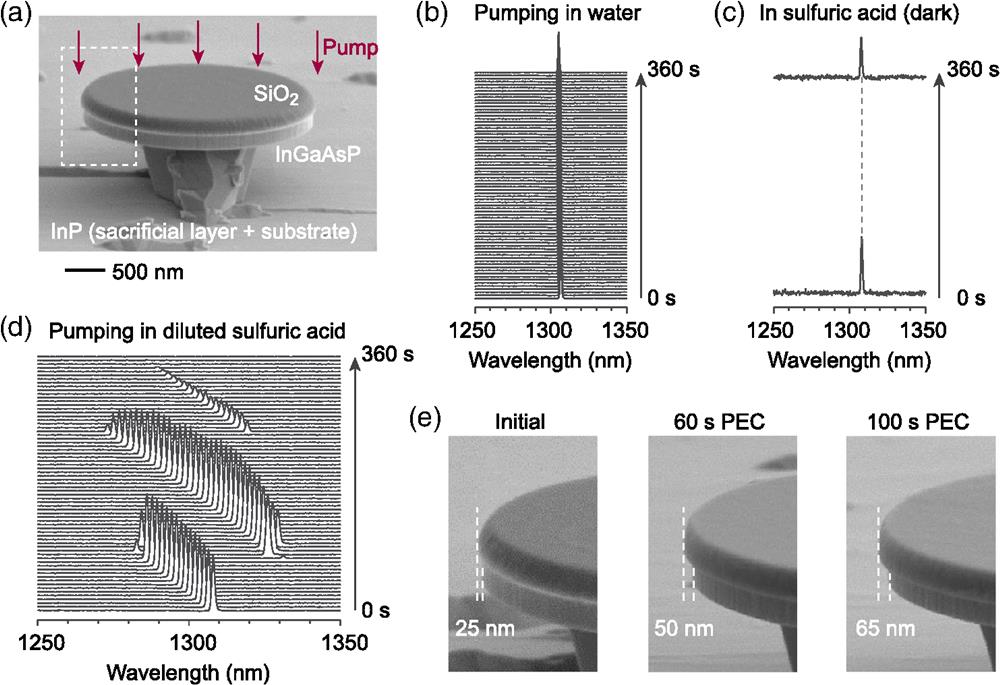
We obtained a custom-ordered semiconductor wafer comprising a 200 nm-thick layer and an InP buffer layer (300 nm thick), both epitaxially grown on an InP substrate using metal organic chemical vapor deposition. The unintentional (n-type) doping concentration of the epitaxial InGaAsP and InP layers is , while the substrate is n-type doped to . To safeguard the top active layer, we deposited a 250 nm-thick layer of using inductively coupled plasma chemical vapor deposition (Oxford ICP-CVD). To improve resist adhesion, we baked the coated wafer at 180°C on a hot plate for 5 min, followed by plasma priming (Anatech SP100). Next, we deposited a -thick photoresist (SU-8 2002, Kayaku) using spin coating. The photoresist was exposed with a quartz photomask having circular patterns using a UV i-line contact aligner (Karl Suss MA6) and then developed to yield resist pillars on the substrate. The photoresist was hard-baked at 190°C to enhance chemical resistance. The microdisk pattern on the photomask was then transferred onto the layer using a chemistry. Next, we removed the photoresist using plasma and a sulfuric acid dip. The mesas were then employed as etch masks to etch non-selectively into the semiconductor using a chemistry (Oxford Instruments ICP-RIE). The etch depth was such that it passed through the InGaAsP layer and penetrated a few hundred nanometers into the underlying InP. We then used a 1:1 dilute hydrochloric acid (HCl) to partially etch the InP (by controlling etching time) underneath the InGaAsP disks, producing a -capped InGaAsP-disk-on-InP-pillar structure. Figure 1(a) shows a representative microdisk on a pillar as seen through scanning electron microscope (SEM).
Figure 1.(a) SEM image of a microdisk-on-pillar structure. Dotted white box indicates region of zoom-in SEM images in (e). Temporal variation of microdisk laser spectrum showing (b) no peak shift with continuous pump laser illumination in water, (c) no peak shift in sulfuric acid under no illumination, and (d) blueshift and mode change of laser peak with continuous illumination in sulfuric acid. (e) SEM images of microdisks before (initial), after 60 s and after 100 s of PEC etching.
To excite charge carriers, we employed a pulsed laser with a wavelength of 1064 nm, 10 ns pulses, and 2 MHz repetition (Spectra Physics VGEN-ISP-POD), which was focused onto a single microdisk with an intensity significantly above the lasing threshold of typical pristine microdisks. The illumination area was large enough to cover the entire disk area. The excitation intensity was adjusted by an acousto-optic modulator and neutral-density filters. The output luminescence of the microdisk was analyzed with a grating-based spectrometer employing a high-speed InGaAs line-scan camera (Sensor Unlimited 2048L).
We immersed microdisks in various solutions to compare the etching speed and light sensitivity of the microdisks. To precisely quantify the degree of etching, we monitored the temporal evolution of the laser emission spectrum from a single microdisk. We found that microdisks are relatively stable in water, both with and without excitation by the pump laser [Fig. 1(b)]. The best results were from a dilute sulfuric acid solution (). Without illumination, the microdisk emission wavelength remained nearly unchanged over a duration of 6 min [Fig. 1(c)]. However, under the continuous illumination of pump light with an intensity of , we observed a relatively rapid shift of the lasing wavelength at a rate of around , as shown in Fig. 1(d). Over time, the microlaser underwent mode hopping and eventually ceased lasing in about 6 min [Fig. 1(d) and Video 1]. Both the blueshift and the mode transition to a lower mode number (indicated by the jump to a longer wavelength) indicate that the diameter of the microdisk continuously reduced during the excitation. SEM images confirmed the reduction of the InGaAsP disk diameter [Fig. 1(e)].
We separately immersed the pristine microdisks in a dilute sulfuric acid bath heated to 200°C and observed no etching of InGaAsP microdisks, indicating that heating alone is not sufficient to induce etching. This result supports the conclusion that the etching mechanism is PEC, rather than photothermal.
2.3 Mechanism of Photoelectrochemical Etching
The PEC etching process in (n-type) III-V semiconductors in an acidic medium typically involves the oxidation of the material, followed by etching of the oxidized material by acid. Under sustained illumination, the anodic reaction results in a reduction in the dimensions of the microdisk, leading to a blueshift of the lasing wavelength. In the case of our study, the InGaAsP material with a bandgap of 0.97 eV absorbs the pump photons at 1064 nm (1.16 eV), generating electrons and holes, while the InP (bandgap 1.34 eV) pillar and substrate do not absorb pump photons. When in contact with the dilute sulfuric acid solution, the InGaAsP layer forms an upward band-bending that leads to charge separation, and holes accumulate near the InGaAsP-solution interface. The holes initiate the oxidation reaction of InGaAsP, producing oxides that are dissolved in the acidic medium.26,27 There are several anodic reactions possible at the surface of InGaAsP, one of which can be written as follows:28,29
On the other hand, photo-induced electrons drift downward in potential from InGaAsP to the undoped InP and then to the n-type InP substrate, from which the electrons are injected into the electrolyte solution, driving the hydrogen evolution reaction. Minimal cathodic dissociation is expected at the surface of n-InP, and the typical water reduction reaction, , prevails. Figure 2(a) illustrates the charge carrier diffusion path (green-red arrow) and representative PEC reactions.
Figure 2.(a) Schematic diagram of a microdisk-on-substrate structure and the flow of electrons and holes enabling redox PEC reactions. (b) Band diagram depicting the energy levels along the charge carrier path between InGaAsP through InP pedestal and InP substrate, with both InGaAsP and InP substrate bounded by the electrolyte solution.
We refer to the band diagram presented in Fig. 2(b), which shows the charge carrier path with the InGaAsP and InP substrate, both bounded by diluted (0.0019 mol/L). The details of the band diagram derivation, including assumptions, are provided in Note S1 in the Supplementary Material. Previous studies have demonstrated30–33 that for PEC etching to occur, a local photovoltaic cell action is required, where one part of the semiconductor is at a more positive potential compared to another region. A uniformly illuminated surface does not create an open-circuit potential difference, which means that no etching occurs. This necessary condition is met in our current structure, where charge carriers are generated in InGaAsP but not generated in the electrically connected InP. This conclusion was further confirmed by releasing microdisks from the InP pillar and dispensing them on an insulating silicon dioxide surface. In this case, PEC etching was nearly absent, as the lasing peak from InGaAsP microdisks stayed at virtually the same wavelength, or blueshifted at orders of magnitude lower rate (Video 2). On the other hand, rapid PEC etching was observed from microdisks released on conductive gold surface (Video 3).
2.4 Kinetics of PEC Etching
The rate equation for photoexcited electron or hole density in intrinsic () or moderately doped () semiconductor can be written as
Here, is the Shockley–Read–Hall recombination coefficient that corresponds to relaxation to traps, including surface defects, is the radiative recombination coefficient, and is the Auger recombination coefficient. The absorption rate of excitation photons is , and represents the carrier loss due to PEC dissociation reactions. The magnitude of this term is substantially smaller than the other terms. We note that , where is the absorption coefficient of excitation light, and is the illumination intensity ( and for 1064 nm).
For InGaAsP disks, we estimate , where is the surface recombination velocity,34 and is the disk radius. We found literature values of and .34 The steady-state solution for in Eq. (1) is
This equation is plotted in Fig. 3(a) as a function of . At low intensity, is linearly proportional to , but it increases sublinearly with when exceeds about .
Figure 3.(a) Theoretical steady-state carrier density as a function of excitation laser intensity based on Eq. (2). (b) Experimental data showing the rate of wavelength changes. (c) Best fit curve based on Eq. (4).
We conducted experimental measurements of the rate of lasing wavelength shift at different pump laser intensities (time-average of the megahertz pulse train) spanning 6 orders of magnitude. The results are presented in Fig. 3(b). To measure wavelength shifts at laser intensities below lasing threshold (), we used a brief pump above threshold while simultaneously collecting the lasing peak position. Then, the pump intensity is lowered to the interrogation value. Finally, the laser was briefly pumped above threshold again while collecting the laser peak position. We obtained the peak wavelength shift by subtracting the starting peak position in the second measurement above threshold from the end peak position in the first measurement above threshold. We observed a sublinear trend in the peak wavelength shift across all incident power levels.
It is well established that a Piranha solution, which contains hydrogen peroxide () as an oxidation agent, can be used to etch InAs, GaAs, and InGaAs, but is less effective for etching InP. Based on this observation, it is reasonable to assume that the dissociation of phosphorus is the rate-limiting step in the dissolution process of InGaAsP in the PEC etching. Since this reaction involves holes [as shown in the equation in Fig. 2(a)], the overall etching rate is proportional to the concentration of photoexcited holes (). However, at higher values of , holes become less efficiently driven to the surface, which leads to a dampening of the etch rate despite the increased generation of electron–hole pairs.33 This effect has been studied in the literature using models that account for charge transport mechanisms within the semiconductor, at the semiconductor–solution interface, and within the solution itself.33,35,36 We have modeled the saturation effects with the following equation: where is the reaction rate coefficient and represents the saturation carrier concentration. The change of radius is equal to the change of lattice constant (equivalent to the length decreased by each dissociation reaction) per reaction times the reaction rate, given by
We fit the experimental data using Eq. (4), as depicted in Fig. 3(c), and obtained and . Using for InGaAsP, we obtain . For example, at , the reaction rate per unit cell is , which means one reaction occurs every 5.3 s per unit cell. It may be noted that the model derived here is independent of the excitation laser operation mode [pulsed or continuous-wave (CW)] and would thus be broadly applicable. While this report focuses primarily on pulsed laser excitation, the same PEC etching can be achieved with CW excitation light sources. Experimentally, we observed PEC etching using a 532 nm CW laser as the excitation source (data not shown).
2.5 Layer-Selective Etching by Excitation Wavelength
We have previously developed wafers containing multiple InGaAsP layers with different alloy compositions, which were used to create random-wavelength LPs.16,17,20,21 By exploiting the different bandgap energies of the individual layers, we can utilize the variation in spectral absorption [ in Eq. (1)] to perform PEC etching on specific layers. To demonstrate this concept, we employed a bilayer wafer composed of (bandgap at 1150 nm) and (bandgap at 1275 nm) layers separated by a 300 nm InP layer. In Fig. 4, we show the effect of bandgap-dependent PEC etching on an array of pillars. Figure 4(a) shows the pillar structure after immersing the chip in dilute sulfuric acid in the dark, where no etching occurs. In Fig. 4(b), we see a chip after exposing it to acidic medium and supercontinuum laser illumination through a long-pass filter that only allows wavelengths greater than 990 nm. The etched pillars indicate that both InGaAsP layers were etched, as evidenced by their reduced diameters between the intact InP layers. It is believed that electrons generated in the upper layer are transported all the way to the substrate. Figure 4(c) shows the same structure under illumination through a long-pass filter at 1250 nm, where the upper InGaAsP layer remained intact, while the lower layer is etched.
Figure 4.SEM images of a bilayer InGaAsP-in-InP pillar structure after immersion in dilute sulfuric acid under different illumination conditions. (a) Without illumination, (b) under illumination with wavelengths >, and (c) under illumination with wavelengths >. Yellow arrows indicate etched InGaAsP layers. Scale bar, .
To ensure reliable PEC tuning, it is critical to protect the flat surface of InGaAsP disks from etching, which is achieved by the capping layer. Figure 5(a) and Fig. S1 in the Supplementary Material present SEM images of microdisks after removal of the silica cap following PEC etching, revealing a normal morphology of the top surface and reasonably smooth sidewalls. When we removed the microdisks from the pillar using HCI etching, we found the bottom surface to be acceptably smooth. While the outer part of the bottom surface is in contact with the etchant solution, the light intensity reaching there is smaller than that on top due to optical absorption throughout the disk thickness, resulting in a less vigorous etch reaction. The overall etch rate for silica-capped disks was measured (from sequence of SEM images) to be ~0.44 nm/s.
Figure 5.(a) SEM images of silica-capped microdisks with PEC etching for 30, 60, and 100 s, with the silica cap removed to show the top and side morphology. Also shown is the bottom surface of a post-PEC microdisk released from its pillar. (b) SEM images of uncapped microdisks after 30 and 60 s of PEC etching, revealing severe top surface roughening. (c), (d) Temporal evolution of lasing peak intensity (mean and standard deviation of five disks) under PEC etch for (c) silica-capped and (d) uncapped microdisks.
In contrast, Fig. 5(b) shows the top surface of microdisks that were etched without silica caps, which visibly affected their morphology with significant surface roughening in 30 s of PEC etch, progressively worsening with longer etch times (Fig. S2 in the Supplementary Material). The porous surface indicates the production of solid components. Uncapped microdisks also show a higher etch rate of ~1.2 nm/s.
The significance of the silica cap is further emphasized by the temporal evolution of the laser peak intensity over an extended period. As shown in Figs. 5(c) and 5(d), the peak intensity initially increases for both silica-capped and non-capped microdisks. In the case of silica-capped disks, this may be attributed to an increase in the factor, as observed in previous studies.24,25 Conversely, for non-silica-capped disks, the observed roughening of the surface suggests that the factor is unlikely to increase. The apparent increase in lasing intensity is instead likely due to an increased scattering of laser light circulating in the disk, as reported in previous studies that employed different engineering methods.37 However, the intensity trend is rather brief for non-capped disks, with the intensity rapidly decreasing after of etching. Silica-capped disks demonstrate higher stability, with peak intensity being retained above the starting intensity for up to 120 s of etching on average.
3 Precision Wavelength Control of Microdisk Lasers
3.1 Subnanometer-Scale Wavelength Control on Disk-on-Chip Lasers
To achieve microlasers with a consistent wavelength, we created a array of microdisks, each with a nominal diameter of arranged in a square lattice of spacing. As shown in the graph labeled (i) in Fig. 6, the initial lasing wavelength distribution of the disks produced by standard nanofabrication spans a range of 9 nm around 1323 nm, which indicates a variation in disk diameter of .16 To address this, we used live-monitoring PEC etching to all the disks to a wavelength 1314.7 nm, and subsequently to 1309.6, 1304.8, and 1299.6 nm (Fig. 6 and Fig. S3 in the Supplementary Material), each time with a standard deviation of 0.5 or 0.6 nm. The median lasing peak intensity in each of these narrowband distribution disks remained close to the starting median peak intensity (see Fig. S4 in the Supplementary Material).
Figure 6.Wavelength tuning by PEC etching. Lasing wavelength histogram of an array of 36 disk-on-pillar samples (i) as fabricated by UV lithography and RIE, and the same array tuned sequentially to give narrowband wavelength distributions of (ii) , (iii) , (iv) , and (v) .
3.2 Nanometer-Scale Wavelength Control of Isolated Laser Particles
In addition, we achieved the fabrication of freestanding LPs by transferring wavelength tuned microdisk arrays onto a polydimethylsiloxane (PDMS) substrate [Fig. 7(a)]. Starting from the microdisk structures on chip, complete etching of InP in dilute HCl released the microdisks in the HCl solution. Then, we centrifuged the LP suspension to collect the disks at the bottom of a tube, and the supernatant liquid was selectively removed. Deionized (DI) water was then added to the tube, and the LPs were redispersed in it by ultrasonication. Repeating this centrifugation, decanting of supernatant, adding fresh DI water, and resuspension of LPs, the medium was effectively cleared of HCl. Freestanding LPs were then obtained by drop-casting the suspension on a PDMS substrate. The wavelength distribution of two separate batches of microdisk LPs released on the PDMS substrate is presented in Fig. 7(b), where the interquartile range is about 1.5 nm. The distribution is compared to the corresponding distribution observed after precision tuning while still on pillars. In both cases, the median lasing wavelength is slightly blueshifted by . This shift is partially attributed to the change in the surrounding medium’s refractive index in the two different situations: the on-pillar measurements were taken with the microdisks surrounded by the etchant solution, while the on-PDMS measurements were taken with one side of the microdisks in contact with the PDMS substrate and the other side by water. The broadening of the distribution for isolated particles is presumably caused by differences in pillar sizes, which affect lasing modes. We believe that the broadening can be reduced through improved engineering.
Figure 7.Isolated microdisk LPs. (a) Optical micrograph showing LPs on a PDMS substrate. (b) Histogram of lasing wavelength of LPs in two different batches after on-chip PEC tuning.
Finally, we explored the application of these precisely tuned LPs for barcoding live cells in culture. Following a similar process as described in the previous section, we obtained freestanding microdisk lasers on a clear-bottom cell-culture well. Normal breast epithelial MCF10A cells were then added in the well. In due course of time, the microdisk lasers were uptaken by the cells, forming an optical barcode for that specific cell. Figure 8(a) shows two LPs, LP1 and LP2, that are taken up by two different cells, remain in the respective cells as the cells continue to thrive and migrate in the culture in their natural cadence. Video 4 is a time-lapse series of pictures showing the entire sequence of events starting from the cells added to the culture well with the LPs already in the well, followed by LPs being naturally uptaken by the respective host cell, and the host cells continuing their natural behavior in the culture media with the associated LP forming their physical optical barcode. These specific LPs were tuned to wavelengths separated from each other by . Figure 8(b) shows the evolution of the lasing wavelength differential of the two LPs in the cell culture over 10 h. As LPs are internalized into cells, small wavelength shifts by up to 0.8 nm are observed. This is due to the adsorption of intracellular proteins on the surface of the LPs, which increases the surrounding refractive index and results in a redshift of the lasing wavelength. This spectral shift can be minimized by thick silica coating.16 For a given silica thickness, the magnitude of the wavelength shift is more or less constant. As a result, the wavelength differential stays stable over this prolonged time period when the LPs are either both outside or inside cells, interspersed with a unique transition signature when the particles were being uptaken by the respective host cells one after the other. This demonstration establishes the functional viability and importance of precision LPs in biomedical applications.
Figure 8.(a) Optical micrograph showing cells with incorporated LPs. One LP (LP1) is internalized by a cell at , and another LP (LP2) is internalized by a different cell at . (b) Lasing wavelength differential of the two microdisk lasers in the cell culture over time.
We have successfully utilized active PEC etching to precisely tune the lasing wavelength of InGaAsP microdisks across a 70 nm gain bandwidth. By applying this technique, we have created precision microdisks that emit lasing within an ultranarrow bandwidth of for on-pillar lasers and for isolated particles. Our model accurately predicted the hole-induced oxidative etching rates based on the illumination intensity. Through automating the wavelength tuning process with a robotic setup, we can potentially achieve single-mode lasers that are precisely tuned deterministically to ultranarrow wavelength bands with higher throughput that can find applications in on-chip photonic communications, information processing, and sensing. In addition, we have observed that freestanding particles isolated after releasing the disks from the pillars retained a narrow distribution with comparable median lasing wavelength values. These high-precision single-mode microdisk LPs have been used to tag live cells and could prove useful in barcoding for specific cell populations and assay molecules.
Video 2. Video (2× speed) of non-tunability of lasing wavelength of an InGaAsP microdisk laser released on (insulating) SiO2 substrate (MP4, 1.58 MB [URL: https://doi.org/10.1117/1.AP.5.5.056004.s2]).
Debarghya Sarkar was a postdoctoral research fellow in Prof. Seok-Hyun Yun’s group at Harvard Medical School and Massachusetts General Hospital at the time of this study. He received his PhD from the University of Southern California (USA) in 2020 and his bachelor’s from Jadavpur University (India) in 2014. His research expertise is in semiconductor materials and devices for electronic, photonic, and biomedical applications. Currently, he is a research engineer at IBM Research.
Paul H. Dannenberg is a medical resident at Mass General Brigham. He received his bachelor’s degrees in physics and computer science from Duke University. He received his PhD in medical engineering and medical physics from MIT and his Doctor of Medicine degree from Harvard Medical School. His main research interest is biomedical imaging with applications to human health.
Nicola Martino received his PhD in physics at Politecnico di Milano in 2015 and is now a scientist at Massachusetts General Hospital and Harvard Medical School. His main interest is in the development of novel laser-based technologies for biomedical applications. His most recent contributions are in the field of laser particles, micron-sized free-standing laser cavities that can be used to barcode and track cells and develop new workflows for single-cell biology.
Kwon-Hyeon Kim is an instructor at the Massachusetts General Hospital, Harvard Medical School, in Boston, USA. He received PhD in materials science and engineering from Seoul National University under the supervision of Prof. Jang-Joo Kim. He completed postdoctoral training at Massachusetts General Hospital, Harvard Medical School (PI Prof. Seok-Hyun Yun), from 2017 to 2022.
Yue Wu received her BS from Zhejiang University of Technology, China, in 2011 and her MS from the University of Chinese Academy of Sciences, China, in 2014. In 2019, she obtained her PhD in chemistry at the Georgia Institute of Technology, USA. She is now a research fellow at Massachusetts General Hospital and Harvard Medical School with Prof. Seok-Hyun Yun. Her current research interest is to develop new micro/nanosized photonic devices to optically barcode individual cells for single-cell spatial and temporal multi-omics.
Seok-Hyun Yun received his PhD in physics from KAIST, Korea, in 1997. He was a Chevening Scholar in 1996, and his thesis research in fiber optics led to a $68M-funded startup, Novera Optics, Inc., in San Jose, California. In 2003, he joined Massachusetts General Hospital and Harvard Medical School where he is now professor, Class of 2016 MGH Research Scholar, and an affiliated faculty member of the Harvard-MIT Division of Health Sciences and Technology at MIT.
[28] G. Kreysa, D. Rauh, K.-I. Ota, R. F. Savinell. Compound semiconductors, electrochemical decomposition. Encyclopedia of Applied Electrochemistry, 238-245(2014).