• Photonics Research
  • Vol. 10, Issue 2, 365 (2022)
Changmin Ahn, Yongjin Na, Minji Hyun, Jinho Bae, and Jungwon Kim*
Author Affiliations
  • School of Mechanical and Aerospace Engineering, Korea Advanced Institute of Science and Technology (KAIST), Daejeon 34141, Republic of Korea
  • show less
    DOI: 10.1364/PRJ.443316 Cite this Article Set citation alerts
    Changmin Ahn, Yongjin Na, Minji Hyun, Jinho Bae, Jungwon Kim. Synchronization of an optical frequency comb and a microwave oscillator with 53 zs/Hz1/2 resolution and 10-20-level stability[J]. Photonics Research, 2022, 10(2): 365 Copy Citation Text show less
    Schematic of EOS-TDs. (a) Sagnac-loop-based EOS-TD with unidirectional phase bias, (b) 3×3 optical coupler-based EOS-TD, (c) DO-MZM-based EOS-TD. VCO, voltage-controlled oscillator; BPD, balanced photodetector; EOM, electro-optic phase modulator; VOA, variable optical attenuator.
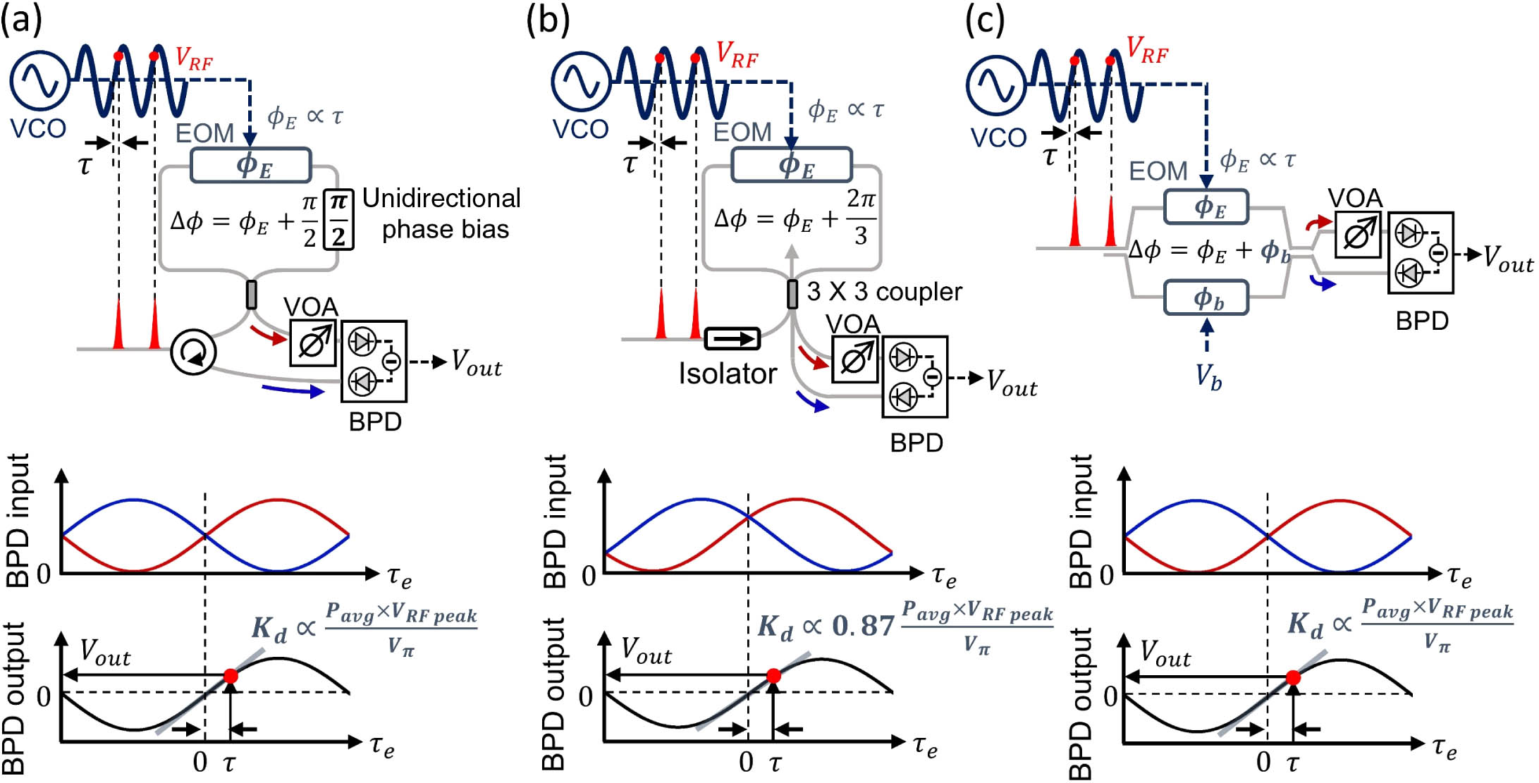
    Fig. 1. Schematic of EOS-TDs. (a) Sagnac-loop-based EOS-TD with unidirectional phase bias, (b) 3×3 optical coupler-based EOS-TD, (c) DO-MZM-based EOS-TD. VCO, voltage-controlled oscillator; BPD, balanced photodetector; EOM, electro-optic phase modulator; VOA, variable optical attenuator.
    Experimental setup schematic of the optical–microwave timing synchronization. DCF, dispersion compensating fiber; MZI, Mach–Zehnder interferometer; LF, loop filter; MDL, manual delay line; BPD, balanced photodetector; PD, photodetector; EDFA, erbium-doped fiber amplifier; RIN, relative intensity noise; LD, laser diode; VCO, voltage-controlled oscillator; BPF, bandpass filter; EOM, electro-optic phase modulator; RF amp, RF amplifier.
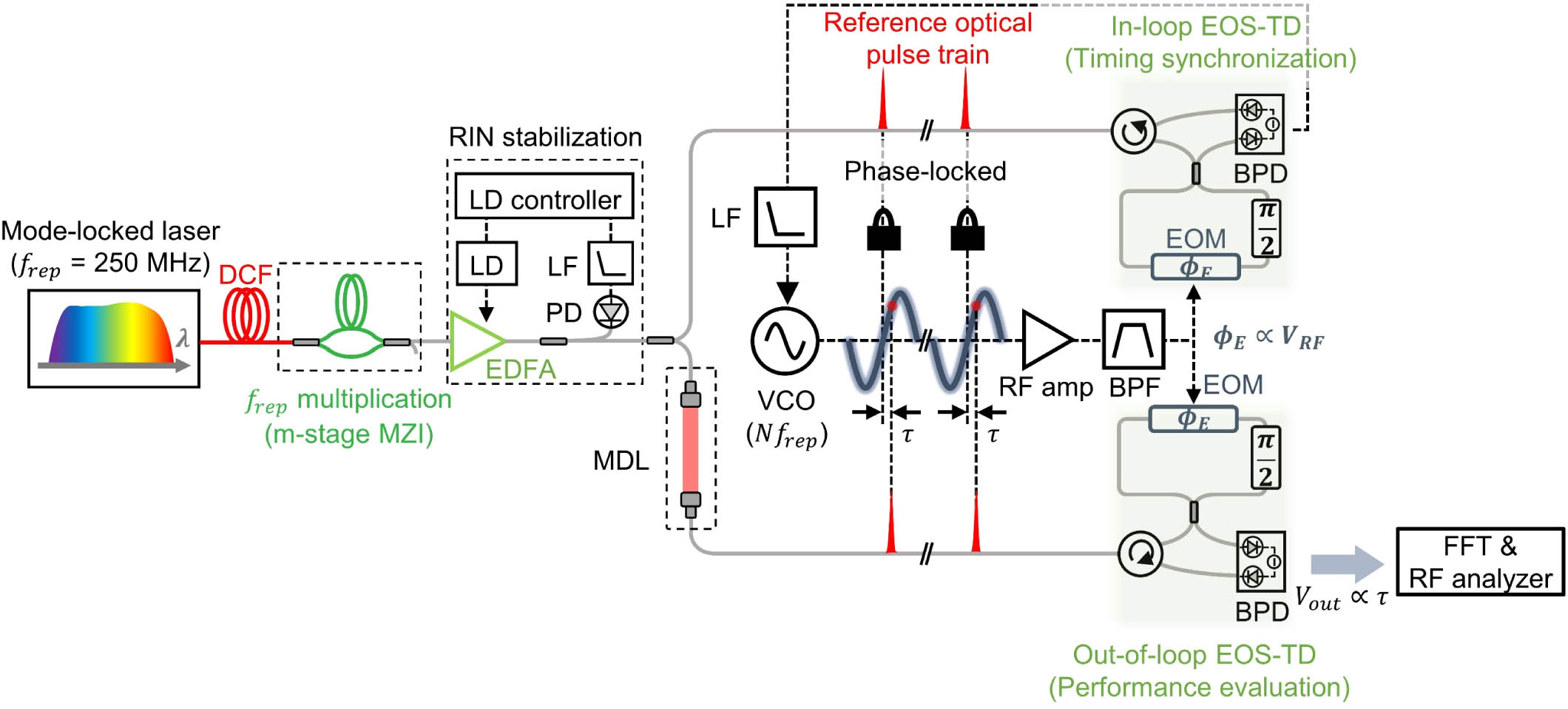
    Fig. 2. Experimental setup schematic of the optical–microwave timing synchronization. DCF, dispersion compensating fiber; MZI, Mach–Zehnder interferometer; LF, loop filter; MDL, manual delay line; BPD, balanced photodetector; PD, photodetector; EDFA, erbium-doped fiber amplifier; RIN, relative intensity noise; LD, laser diode; VCO, voltage-controlled oscillator; BPF, bandpass filter; EOM, electro-optic phase modulator; RF amp, RF amplifier.
    (a) RF spectrum of the 8 GHz VCO output without (black) and with RF bandpass filtering (red). (b) SSB residual phase noise at 8 GHz carrier [curve (i), curve (iii)] without and [curve (ii), curve (iv)] with the RF bandpass filter when repetition rate is 250 MHz and 2 GHz, respectively. Here, the dashed line is the shot limit of the in-loop EOS-TD.
    Fig. 3. (a) RF spectrum of the 8 GHz VCO output without (black) and with RF bandpass filtering (red). (b) SSB residual phase noise at 8 GHz carrier [curve (i), curve (iii)] without and [curve (ii), curve (iv)] with the RF bandpass filter when repetition rate is 250 MHz and 2 GHz, respectively. Here, the dashed line is the shot limit of the in-loop EOS-TD.
    (a) Change of detection sensitivity for different pulse repetition rates. (b) SSB phase noise floor at 8 GHz carrier [curve (i)] without MZI, [curve (ii)] with 1-stage, [curve (iii)] 2-stage, and [curve (iv)] 3-stage MZI, respectively.
    Fig. 4. (a) Change of detection sensitivity for different pulse repetition rates. (b) SSB phase noise floor at 8 GHz carrier [curve (i)] without MZI, [curve (ii)] with 1-stage, [curve (iii)] 2-stage, and [curve (iv)] 3-stage MZI, respectively.
    SSB phase noise at 8 GHz carrier and integrated timing jitter with the experimental setup of Fig. 1. Curve (i) denotes the phase noise of free-running VCO, curve (ii) denotes the phase noise after timing synchronization, and curve (iii) denotes the measurement background of the out-of-loop EOS-TD. The dashed line is a calculated shot-noise limit of the in-loop EOS-TD. The red line at the bottom graph indicates the integrated timing jitter of curve (ii).
    Fig. 5. SSB phase noise at 8 GHz carrier and integrated timing jitter with the experimental setup of Fig. 1. Curve (i) denotes the phase noise of free-running VCO, curve (ii) denotes the phase noise after timing synchronization, and curve (iii) denotes the measurement background of the out-of-loop EOS-TD. The dashed line is a calculated shot-noise limit of the in-loop EOS-TD. The red line at the bottom graph indicates the integrated timing jitter of curve (ii).
    SSB residual phase noise at 8 GHz carrier and integrated timing jitter. Curve (i), curve (ii) indicate the residual phase noise with and without the lead compensator, respectively. The phase noise of the VCO is also shown [curve (iii)]. Integrated timing jitters of curves (i), (ii) correspond to blue and red curves, respectively.
    Fig. 6. SSB residual phase noise at 8 GHz carrier and integrated timing jitter. Curve (i), curve (ii) indicate the residual phase noise with and without the lead compensator, respectively. The phase noise of the VCO is also shown [curve (iii)]. Integrated timing jitters of curves (i), (ii) correspond to blue and red curves, respectively.
    Long-term stability evaluation results. (a) Relative timing error measured for 12 h, (b) residual phase noise and integrated jitter down to 1 mHz offset frequency, and (c) fractional frequency instability (overlapping Allan deviation).
    Fig. 7. Long-term stability evaluation results. (a) Relative timing error measured for 12 h, (b) residual phase noise and integrated jitter down to 1 mHz offset frequency, and (c) fractional frequency instability (overlapping Allan deviation).
    Changmin Ahn, Yongjin Na, Minji Hyun, Jinho Bae, Jungwon Kim. Synchronization of an optical frequency comb and a microwave oscillator with 53 zs/Hz1/2 resolution and 10-20-level stability[J]. Photonics Research, 2022, 10(2): 365
    Download Citation