• Laser & Optoelectronics Progress
  • Vol. 58, Issue 10, 1011009 (2021)
Runyu Huang1、2、**, Weilin Zhao1、2, Hui Zeng1、2, Zaibo Li1、2, Zepeng Hou1、2, Haifeng Ye1、2, Wei Wang1、2, Jiaxin Zhang1、2, Chen Liu1、2, Xueyan Yang1、2, Hongxia Zhu1、2, Yanli Shi1、2、*, and Yuntian Jiang3
Author Affiliations
  • 1School of Physics and Astronomy, Yunnan University, Kunming, Yunnan 650091, China
  • 2Key Laboratory of Quantum Information of Yunnan Province, Yunnan University, Kunming, Yunnan 650091, China
  • 3PLA 96901, Unit 24, Beijing 100094, China
  • show less
    DOI: 10.3788/LOP202158.1011009 Cite this Article Set citation alerts
    Runyu Huang, Weilin Zhao, Hui Zeng, Zaibo Li, Zepeng Hou, Haifeng Ye, Wei Wang, Jiaxin Zhang, Chen Liu, Xueyan Yang, Hongxia Zhu, Yanli Shi, Yuntian Jiang. Development and Application of InP-Based Single Photon Detectors[J]. Laser & Optoelectronics Progress, 2021, 58(10): 1011009 Copy Citation Text show less
    Structure of diffused junction GM-APD
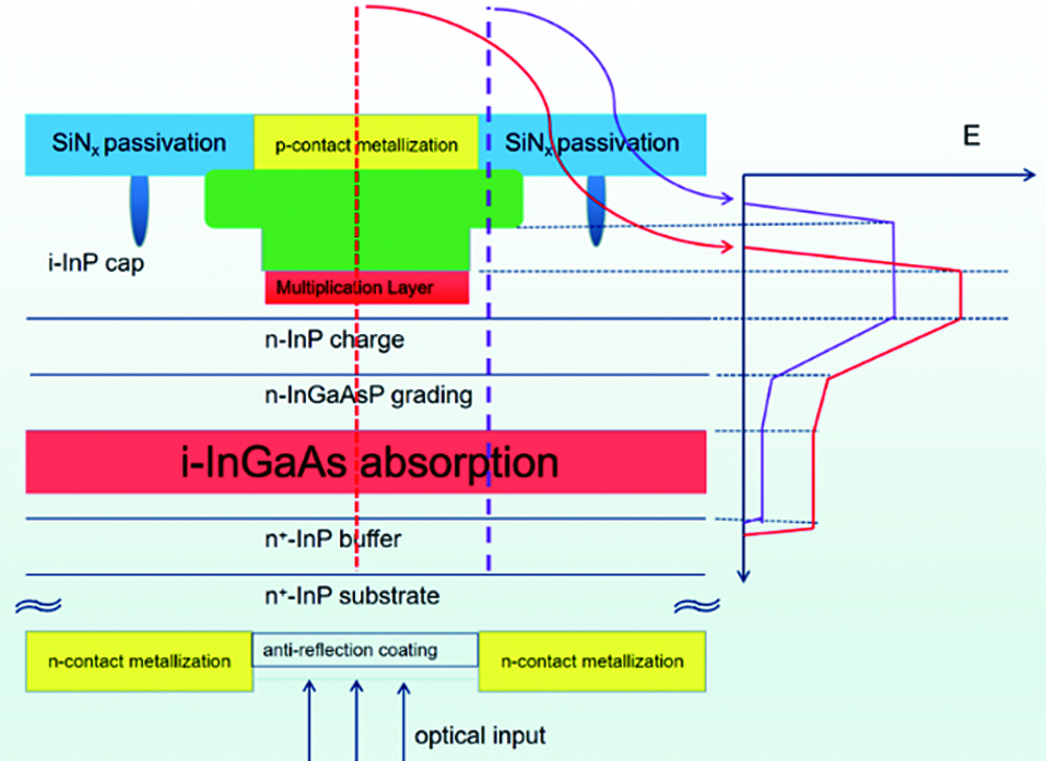
    Fig. 1. Structure of diffused junction GM-APD
    Relationship between gate amplitudes, temperatures, and normalized DCR, afterpulse probablity and PDE. (a) SPAD #1; (b) SPAD #2 [8]
    Fig. 2. Relationship between gate amplitudes, temperatures, and normalized DCR, afterpulse probablity and PDE. (a) SPAD #1; (b) SPAD #2 [8]
    Relationship between excess noise and device gain
    Fig. 3. Relationship between excess noise and device gain
    Measurement curves under 2 μm illumination at room temperature. (a) Device A; (b) device B[17]
    Fig. 4. Measurement curves under 2 μm illumination at room temperature. (a) Device A; (b) device B[17]
    MAGIC detector. (a) MAGIC detector equivalent circuit; (b) an exemplary design of the MAGIC detector with InGaAs/InP material[19]
    Fig. 5. MAGIC detector. (a) MAGIC detector equivalent circuit; (b) an exemplary design of the MAGIC detector with InGaAs/InP material[19]
    Results of Monte Carlo simulation. (a) Distribution of single-photon current response from Monte Carlo simulations; (b) dependence of current output on the number of photons in the input signal[19]
    Fig. 6. Results of Monte Carlo simulation. (a) Distribution of single-photon current response from Monte Carlo simulations; (b) dependence of current output on the number of photons in the input signal[19]
    Structure and working principle of self-quenching and self-recovery detector. (a) Structure; (b) working principle[22]
    Fig. 7. Structure and working principle of self-quenching and self-recovery detector. (a) Structure; (b) working principle[22]
    NFAD top integrated resistance[26]
    Fig. 8. NFAD top integrated resistance[26]
    Relationship between afterpulse probability and PDE of the self quenching SPADs with monolithic integrated passive quenching resistor[27]
    Fig. 9. Relationship between afterpulse probability and PDE of the self quenching SPADs with monolithic integrated passive quenching resistor[27]
    1024 pixel performance maps of InGaAs/InP (1.55 μm) SPADs 32 × 32 focal plane arrays. (a) DCR of all pixels is kHz, less than 50 kHz; (b) average pixel PDE is 22%, taking into account all optical losses related to microlens array and other insertion[27]
    Fig. 10. 1024 pixel performance maps of InGaAs/InP (1.55 μm) SPADs 32 × 32 focal plane arrays. (a) DCR of all pixels is kHz, less than 50 kHz; (b) average pixel PDE is 22%, taking into account all optical losses related to microlens array and other insertion[27]
    Relevant parameters and cross section diagram of GM-APD. (a) Relationship between PDE,crosstalk and over bias of GM-APD; (b) cross section of InP GM-APD array combined with MLA[31]
    Fig. 11. Relevant parameters and cross section diagram of GM-APD. (a) Relationship between PDE,crosstalk and over bias of GM-APD; (b) cross section of InP GM-APD array combined with MLA[31]
    1×16 InGaAs/InP SPAD line array[34]
    Fig. 12. 1×16 InGaAs/InP SPAD line array[34]
    Schematic of optical path between two pixels. (a) Without metal trenches; (b) with metal trenches[34]
    Fig. 13. Schematic of optical path between two pixels. (a) Without metal trenches; (b) with metal trenches[34]
    Schematic cross section and electric field profile of Alx In1-x Asy Sb1-y SAGCM APD[41]
    Fig. 14. Schematic cross section and electric field profile of Alx In1-x Asy Sb1-y SAGCM APD[41]
    External quantum efficiency versus wavelength of a 150-μm-diameter AlxIn1-xAsySb1-y SAGCM APD at 300 K[41]
    Fig. 15. External quantum efficiency versus wavelength of a 150-μm-diameter AlxIn1-xAsySb1-y SAGCM APD at 300 K[41]
    EQE as a function of wavelength at 27 V and 23 V reverse bias for devices A and B, respectively[17]
    Fig. 16. EQE as a function of wavelength at 27 V and 23 V reverse bias for devices A and B, respectively[17]
    Current-voltage and gain. (a) Devices A; (b) devices B[17]
    Fig. 17. Current-voltage and gain. (a) Devices A; (b) devices B[17]
    Device structure diagram and energy band arrangement of Ga0.47In0.53As/GaAs0.51Sb0.49[43]
    Fig. 18. Device structure diagram and energy band arrangement of Ga0.47In0.53As/GaAs0.51Sb0.49[43]
    Relationship between dark current and reverse bias voltage of 200 μm devices[43]
    Fig. 19. Relationship between dark current and reverse bias voltage of 200 μm devices[43]
    Image of InGaAs / InP GM-APD 32 × 32 array. (a) 800 m target and imaging; (b) 6800 m target and imaging[47]
    Fig. 20. Image of InGaAs / InP GM-APD 32 × 32 array. (a) 800 m target and imaging; (b) 6800 m target and imaging[47]
    PurposeThickness /mmMaterialTypeDoping density /cm-3
    Contact20In0.53Ga0.47Asp+1019
    Cladding500In0.53Ga0.47Asp+2×10¹⁸
    45In0.53Ga0.47Asi--
    Absorber15005 nm In0.53Ga0.47As /5 nm GaAs0.51Sb0.49i--
    50In0.53Ga0.47Asi--
    Grading50InAlGaAs(1 eV)i--
    Charge sheet110In0.52Al0.48Asp3×1017
    Multiplication1000In0.52Al0.48Asi--
    Cladding500In0.53Ga0.47Asn+2×10¹⁸
    Substrate--InPn+--
    Table 1. Parameters of device layer structure[44]
    Runyu Huang, Weilin Zhao, Hui Zeng, Zaibo Li, Zepeng Hou, Haifeng Ye, Wei Wang, Jiaxin Zhang, Chen Liu, Xueyan Yang, Hongxia Zhu, Yanli Shi, Yuntian Jiang. Development and Application of InP-Based Single Photon Detectors[J]. Laser & Optoelectronics Progress, 2021, 58(10): 1011009
    Download Citation