Abstract
With the emergence of new materials for high-efficiency organic solar cells (OSCs), understanding and finetuning the interface energetics become increasingly important. Precise determination of the so-called pinning energies, one of the critical characteristics of the material to predict the energy level alignment (ELA) at either electrode/organic or organic/organic interfaces, are urgently needed for the new materials. Here, pinning energies of a wide variety of newly developed donors and non-fullerene acceptors (NFAs) are measured through ultraviolet photoelectron spectroscopy. The positive pinning energies of the studied donors and the negative pinning energies of NFAs are in the same energy range of 4.3?4.6 eV, which follows the design rules developed for fullerene-based OSCs. The ELA for metal/organic and inorganic/organic interfaces follows the predicted behavior for all of the materials studied. For organic–organic heterojunctions where both the donor and the NFA feature strong intramolecular charge transfer, the pinning energies often underestimate the experimentally obtained interface vacuum level shift, which has consequences for OSC device performance.With the emergence of new materials for high-efficiency organic solar cells (OSCs), understanding and finetuning the interface energetics become increasingly important. Precise determination of the so-called pinning energies, one of the critical characteristics of the material to predict the energy level alignment (ELA) at either electrode/organic or organic/organic interfaces, are urgently needed for the new materials. Here, pinning energies of a wide variety of newly developed donors and non-fullerene acceptors (NFAs) are measured through ultraviolet photoelectron spectroscopy. The positive pinning energies of the studied donors and the negative pinning energies of NFAs are in the same energy range of 4.3?4.6 eV, which follows the design rules developed for fullerene-based OSCs. The ELA for metal/organic and inorganic/organic interfaces follows the predicted behavior for all of the materials studied. For organic–organic heterojunctions where both the donor and the NFA feature strong intramolecular charge transfer, the pinning energies often underestimate the experimentally obtained interface vacuum level shift, which has consequences for OSC device performance.1. Introduction
Organic semiconductors, promising candidates for the next generation electronic devices, are already used in versatile applications such as organic light-emitting diodes[1], organic field-effect transistors[2], organic photodetectors[3–5], and organic solar cells (OSCs)[6], owing to their advantages of light weight, flexibility, semi-transparency, tunable optical gaps and energy levels[7]. In the field of OSCs, great efforts have been devoted to the synthesis of new donors (D) and acceptors (A) with optimal energy level alignment (ELA) at both electrode and D–A interfaces[8–13]. However, the interface electronic properties and the corresponding influences on the charge generation and charge collection are not fully understood[14], especially for those recently developed non-fullerene acceptor (NFA) based systems, which hampers further material design and device optimization of OSCs.
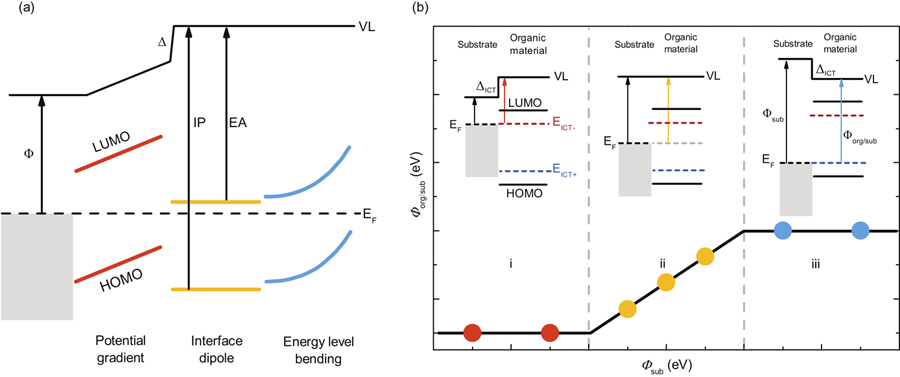
To understand the interface energetics in OSCs, the fundamental task prior to drawing the energy-level diagram is correctly determining the energies of the highest occupied molecular orbital (HOMO) and the lowest unoccupied molecular orbital (LUMO) of a material, corresponding to the edges of hole and electron conduction levels with reference to the vacuum level, which defines the ionization energies (IP) and electron affinities (EA) of the material, respectively[15]. However, the information of HOMO and LUMO levels only is far more enough to depict the ELA at interfaces due to the complicated but normally existed interface phenomenon such as potential gradient, interface dipoles, energy level bending, and so on (Fig. 1(a)). It should be noted that the commonly used energy-level diagrams in literatures usually assume vacuum level (VL) alignment without taking the interface phenomenon into consideration. This can be misleading, since the VL alignment at such interfaces is rather the exception than the rule[16]. Instead, VL shifts (i.e., work function (Φ) change) is quite a normal phenomenon, which is usually caused by an interface dipole formed in order to equilibrate a chemical potential difference at the interface.

Figure 1.(Color online) (a) Schematic of the common interface phenomenon at organic/metal or organic/organic interfaces. (b) Schematic illustration of the integer charge transfer (ICT) model.
The integer charge transfer (ICT) model predicts the size and direction of interface dipole induced VL-shifts at weakly interacting metal/organic and organic/organic interfaces based on the so-called pinning energies (positive pinning energies,, and negative pinning energies,)[17,18], which has been widely used to explain and tune interface phenomenon in OSC devices[19–23]. Specifically, the positive (negative) pinning energy is the energy required for a material to be oxidized (reduced) forming a fully relaxed positive (negative) polaronic state at the interface. Here, the fully relaxed polaronic states refer to the states after the polaron’s electronic and geometrical relaxation, as well as the screening from the environment and the Coulombic interaction with the opposite charge across the interface, which are pushed into the gap compared to the bulk IP (EA), as shown inFig. 1(b). Based on the ICT model, the chemical potential difference at an interface is equilibrated by the spontaneous oxidation or reduction of the molecules where the subsequent charge transfer across the interface creates a potential step (∆) that shifts the VL[18]. The resulting ELA for the interface can be divided into three scenarios (Fig. 1(b)): (i) when the work function of the substrateΦsub is smaller than of the organic material,Φsub \lt, electrons will transfer from substrate to the organic material, contributing to a VL upshift (∆ = –Φsub) with Fermi-level pinning to; (ii) when \ltΦsub \lt, no electron transfer will occur between the substrate and the organic material, thus VL alignment will be shown without interface dipoles (∆ = 0 eV), and the work function of organic-on-substrateΦorg/sub will linearly depend onΦsub with a slope of 1; (iii) whenΦsub \gt, electrons will flow from organic material to the substrate, resulting in a downshift of VL (∆ =Φsub –) with Fermi-level pinning to[17,18].
The pinning energies of the donors or acceptors are important parameters to both determine and design the ELA at both the electrode-active layer interface and the D–A interface in OSCs. Pinning energies of many traditional organic semiconductors have been already reported[21,24–27], but few reports are focused on the newly developed NFA based D–A systems. In this paper, we utilize ultraviolet photoelectron spectroscopy (UPS) to determine the pinning energies and IPs of a batch of donors and acceptors applied in high-efficiency OSCs. It is found that all the studied materials follow the general ELA trend predicted by the ICT model when deposited onto the inert conducting substrates. The positive pinning energies of the studied donors and the negative pinning energies of NFAs almost sit at the similar energy level of around 4.3−4.6 eV, which follows the established design rules for fullerene-based D–A systems. However, recent results show that for D–A combinations where both the NFA and the donor feature strong intramolecular charge transfer, the interface VL shift is typically significantly larger than that predicted by the ICT model, which then also affect OSC device performance as we comment on here.
2. Methods
To determine the pinning energies of a material, work functions of several conductive substrates should be determined by UPS prior to the organic semiconductor film deposition. The substrates commonly used are: gold (Au) exposed to air (Φsub = 4.5–4.6 eV) or UV/ozone (UVO)-treated Au (Φsub = 5.2–5.7 eV), PEDOT:PSS (Φsub = 5.0–5.1 eV), indium tin oxide (ITO) as-received (Φsub = 4.5–4.7 eV) or UVO-treated (Φsub = 4.7–5.0 eV), SiOx/Si (Φsub = 4.1–4.7 eV), ZnO/ITO (Φsub = 3.8–4.1 eV), AlOx/Al (Φsub = 3.4–3.9 eV). Then the organic semiconductor material is spin-coated on these substrates of different work functions and is transferred for UPS measurements. AsFig. 2(a) shows, after determining the work function of a substrate from the secondary-electron cutoff edge (Ecutoff) by using the simple formula:Φ =hν –Ecutoff, work function of the same material-coated substrate is remeasured, so a change in work function or a potential step∆ can be obtained. Meanwhile the vertical IP of the material can be derived from the frontier edge of the valence band spectrum (EVB) by using formula: IP =EVB +Φ. The spectra of Y11 coated on different substrates are shown as an example inFig. 2(b), and spectra of other materials are shown in Fig. S1 of the Supporting Information. The UPS measurements are carried out under the standard conditions as we mentioned in previous works[28,29]. Layer-by-layer deposition of polymer films using Langmuir-Blodgett or Langmuir-Schäfer techniques have demonstrated that the interface potential step∆ is abrupt, typically extending over only 2–3 monolayers with most of the shift obtained already after one monolayer[28,29].
Figure 2.(Color online) (a) Schematic illustration of deriving important parameters from UPS characterization. (b) UPS spectra of Y11 spin-coated on different substrates. The spectra of negative pinning region, vacuum level alignment region and positive pinning region are denoted in red, yellow, and blue, respectively.
3. Results and discussion
Having the work function values of both bare substrates,Φsub, and the corresponding material-coated substrates,Φorg/sub in hand, one can easily get the relationship betweenΦorg/sub andΦsub. As can be seen inFig. 3,Φorg/sub is plotted againstΦsub for various materials including donors and NFAs developed in recent years. It shows that all the studied organic semiconductor materials follow the ICT model, where three regions of ELA at the interface between the inert substrates and organic semiconductors are shown: (i) Fermi-level pinning to (slope = 0) region at low work function substrates, (ii) vacuum-level alignment (slope = 1) region at moderate work function substrates, and (iii) Fermi-level pinning to (slope = 0) region at high work function substrates, although the region i where sits could not be reached for most of the donors due to the lack of air-stable substrates with ultra-low work functions (Φsub \lt 3.4 eV). The of donors and acceptors are derived from the averageΦorg/sub values of data points at the plateau region of Fermi-level pinning ( from region iii, from region i) whereΦorg/sub is independent onΦsub. The resulting pinning energy values of the range of materials are summarized inTable 1. Following this basic pinning energy information of these materials, one can easily determine the ELA at the related electrode/organic interface to further figure out the energy barriers for charge collection or charge injection at the electrodes in several organic electronic devices[30–32].
Figure 3.(Color online) Dependence of the work function of (a) donor and (b) NFA coated substrates (Φorg/sub) on the work function of bare substrate (Φsub). Data points of PM6, PBDB-T, ITIC, and IT4F are abstracted from Ref. [29].
Table Infomation Is Not Enable
For most donors inFig. 3(a), the positive pinning energies all locate in the energy range of 4.3−4.6 eV (shadowed region in light green), which is almost the same level range as the negative pinning energies (shadowed region in light green) of the NFAs inFig. 3(b). Based on the ICT model, vacuum level alignment (∆ = 0 eV, when \gt) or small interface dipoles (∆ = –, when \lt) would be predicted at the interfaces of these D–A pairs. This suggests efficient charge generation and small voltage loss in bulk heterojunctions based on the design rules for fullerene-based OSC devices proposed in our previous works[19,21,22]. According to the previous investigation on the relationship between the voltage loss and the ICT dipoles of various fullerene-based D–A systems, it is found that charge recombination could be suppressed at the sweet point where the positive pinning energy of the donor roughly equals to the negative pinning energy of the acceptor, ≈, otherwise trap-assisted recombination via ICT states at D–A interfaces would be dominant when \lt, or free charge generation would be less efficient in the absence of ICT dipoles at D–A interfaces when \gt. This empirical design rule has been proved to be useful for understanding the voltage loss mechanisms in OSCs based on the old type donors, fullerene acceptors, and even some NFAs[21,22]. For example, when P3HT (EICT+ = 4.14 eV) is paired with most acceptors like C60, PC70BM, ITIC and IT4F, with of 4.57, 4.40, 4.42, 4.55 eV, respectively, large ICT dipoles of around 0.3−0.4 eV are obtained at these D–A interface. In these cases, misalignment of and will lead to prominent density of occupied ICT states (and interface potential step) at the D–A interfaces already at dark conditions, where then photo-generated free electrons (holes) in the acceptor (donor) domains would combine with the () related positive (negative) polarons at the donor (acceptor) side of the interface, resulting in increased voltage loss. Thus, the low lying of P3HT might be one of the bottlenecks hindering the further improvement on device efficiency. However, two strategies could be employed to diminish the negative influence from the ICT states at interfaces: first, thermal or solvent annealing can be used to decrease the ICT dipoles at the D–A interfaces by enhancing the donor[22]; second, pairing P3HT with acceptors of low, like IC60BA ( = 4.05 eV), O-IDTBR ( = 4.16 eV) is helpful to improve the PCEs[21,33,34] as it matches the with the.
The ICT model has been proven very robust in predicting metal/organic, inorganic/organic and organic/organic interface ELA. However, recent results on the newly developed D–A systems where both donors and acceptors featuring so-called push-pull structures (intramolecular charge transfer) suggest that the ICT model is insufficient to explain the measured D–A interface ELA[29]. The ELA at well-defined D–A interface based on high-efficiency NFA systems were determined in a layer-by-layer manner through the Langmuir-Schäfer technique and the results show that significant interface dipoles exist at these D–A interfaces based on D–A pairs featuring push-pull structure and large HOMO difference prior to contact, even though the pinning energy of donor match with that of the acceptor. This finding contradicts the ICT model prediction of small or even zero interface dipoles at these particular D–A interfaces. The presence of the prominent interface dipoles up-shifts the HOMO and LUMO of the NFAs at the D–A interface, leading to a reduction in the interfacial energy level offsets and an increase in charge transfer state energies (ECT), as shown in the schematic illustration inFig. 4. The ELA diagram corrected with the measured interface dipole (ELA after D–A contact) reflects the real situation in devices as demonstrated by theECT obtained from several OSCs. It is interesting to compare the D–A interfaces based on the old-type OSC materials where ELA follows the ICT model with the D–A interfaces based on new-type materials with push-pull structures where the ELA does not follow the ICT model. In the former case, a significant D–A interface VL shift that brings the benefits of increasedECT from the up-shifting of the acceptor HOMO/LUMO levels and enhanced exciton dissociation[19,35], also brings penalties in the form of increased recombination losses induced by the (dark) ICT state density that creates the VL shift. Hence the experimentally observed “sweet-spot” is reached at ≈. For the new NFA-donor systems, a significant VL up-shift can be obtained even though ≈, so an increasedECT and enhanced exciton dissociation efficiency is obtained without paying the penalty of ICT-state-induced recombination that decreases the open circuit voltage. This suggests that pursuing engineering of the D–A interface to obtain VL up-sifts while avoiding the creation of interface ICT states ( ≥) is a possible route to achieve better performing OSCs.
Figure 4.(Color online) Schematic illustration of energy levels of donor and acceptor before and after contact. ΔHOMO (Δ′HOMO), ΔLUMO (Δ′LUMO), Γ(Γ′) present the HOMO difference, LUMO difference, and interfacial state energy gap before (after) the donor (D) and acceptor (A) contact. Δ is the interface dipole inducing the vacuum level (VL) shift.
4. Conclusion
In summary, the pinning energies of a wide variety of organic semiconductor materials used in high-efficiency OSCs are characterized. The ELA for metal/organic and inorganic/organic interfaces follows the ICT model for all materials studied, demonstrating its utility for designing electrode and charge-transport-layer interfaces. The positive pinning energies of the studied donors are in the similar range as the negative pinning energies of the NFAs, sitting at around 4.3−4.6 eV, which follows the design rules for fullerene-based OSCs. The ICT model fails, however, at predicting organic/organic D–A interfaces involving donors and NFAs both featuring strong “push-pull” nature. Interestingly, for these systems a significant interface VL-shift can be obtained even when a (near) zero interface dipole is predicted by the ICT model due to the absence of induced ICT states at the D–A interface. This enables the NFA-based OSCs to gain the benefits of increasedECT and exciton dissociation efficiency without paying the price of increased trap-induced recombination.
Appendix A. Supplementary materials
Supplementary materials to this article can be found online athttps://doi.org/10.1088/1674-4926/44/3/032201.
References
[1] G Hong, X Gan, C Leonhardt et al. A brief history of OLEDs—emitter development and industry milestones. Adv Mater, 33, 2005630(2021).
[2] L Torsi, M Magliulo, K Manoli et al. Organic field-effect transistor sensors: a tutorial review. Chem Soc Rev, 42, 8612(2013).
[3] H Ren, J De Chen, Y Q Li et al. Recent progress in organic photodetectors and their applications. Adv Sci, 8, 2002418(2021).
[4] Z Zhao, B Liu, C Xie et al. Highly sensitive, sub-microsecond polymer photodetectors for blood oxygen saturation testing. Sci Chin, 64, 1302(2021).
[5] Z Zhao, C Xu, Y Ma et al. Ultraviolet narrowband photomultiplication type organic photodetectors with Fabry−Pérot resonator architecture. Adv Funct Mater, 32, 2203606(2022).
[6] P Cheng, G Li, X Zhan et al. Next-generation organic photovoltaics based on non-fullerene acceptors. Nat Photonics, 12, 131(2018).
[7] Y Liang, D Feng, Y Wu et al. Highly efficient solar cell polymers developed via fine-tuning of structural and electronic properties. J Am Chem Soc, 131, 7792(2009).
[8] S Li, L Ye, W Zhao et al. A wide band gap polymer with a deep highest occupied molecular orbital level enables 14.2% efficiency in polymer solar cells. J Am Chem Soc, 140, 7159(2018).
[9] Y Xu, Y Cui, H Yao et al. A new conjugated polymer that enables the integration of photovoltaic and light-emitting functions in one device. Adv Mater, 33, 2101090(2021).
[10] J Qin, L Zhang, C Zuo et al. A chlorinated copolymer donor demonstrates a 18.13% power conversion efficiency. J Semicond, 42, 010501(2021).
[11] H Yang, C Cui, Y Li. Effects of heteroatom substitution on the photovoltaic performance of donor materials in organic solar cells. Accounts Mater Res, 2, 986(2021).
[12] W Xu, X Li, S Y Jeong et al. Achieving 17.5% efficiency for polymer solar cells via a donor and acceptor layered optimization strategy. J Mater Chem C, 10, 5489(2022).
[13] W Xu, X Zhu, X Ma et al. Achieving 15.81% and 15.29% efficiency of all-polymer solar cells based on layer-by-layer and bulk heterojunction structures. J Mater Chem A, 10, 13492(2022).
[14] Y Liu, Y Wu, Y Geng et al. Managing challenges in organic photovoltaics: properties and roles of donor/acceptor interfaces. Adv Funct Mater, 32, 2206707(2022).
[15] J Bertrandie, J Han, C S P De Castro et al. The energy level conundrum of organic semiconductors in solar cells. Adv Mater, 34, 2202575(2022).
[16] S Duhm. Interface energetics in organic electronic devices. Elsevier, 143(2021).
[17] B S Braun, W R Salaneck, M Fahlman. Energy-level alignment at organic/metal and organic/organic interfaces. Adv Mater, 21, 1450(2009).
[18] M Fahlman, S Fabiano, V Gueskine et al. Interfaces in organic electronics. Nat Rev Mater, 4, 627(2019).
[19] H Aarnio, P Sehati, S Braun et al. Spontaneous charge transfer and dipole formation at the interface between P3HT and PCBM. Adv Energy Mater, 1, 792(2011).
[20] M Fahlman, P Sehati, W Osikowicz et al. Photoelectron spectroscopy and modeling of interface properties related to organic photovoltaic cells. J Electron Spectrosc Relat Phenom, 190, 33(2013).
[21] Q Bao, O Sandberg, D Dagnelund et al. Trap-assisted recombination via integer charge transfer states in organic bulk heterojunction photovoltaics. Adv Funct Mater, 24, 6309(2014).
[22] C Wang, F Moro, S Ni et al. Thermal-annealing effects on energy level alignment at organic heterojunctions and corresponding voltage losses in all-polymer solar cells. Nano Energy, 72, 104677(2020).
[23] D Li, L Zhu, X Liu et al. Enhanced and balanced charge transport boosting ternary solar cells over 17% efficiency. Adv Mater, 32, 2002344(2020).
[24] C Tengstedt, W Osikowicz, W R Salaneck et al. Fermi-level pinning at conjugated polymer interfaces. Appl Phys Lett, 88, 053502(2006).
[25] L Lindell, D Çakr, G Brocks et al. Role of intrinsic molecular dipole in energy level alignment at organic interfaces. Appl Phys Lett, 102, 223301(2013).
[26] C Wang, X Xu, W Zhang et al. Ternary organic solar cells with enhanced open circuit voltage. Nano Energy, 37, 24(2017).
[27] C Wang, S Ni, S Braun et al. Effects of water vapor and oxygen on non-fullerene small molecule acceptors. J Mater Chem C, 7, 879(2019).
[28] Q Bao, S Fabiano, M Andersson et al. Energy level bending in ultrathin polymer layers obtained through Langmuir-Shäfer deposition. Adv Funct Mater, 26, 1077(2016).
[29] X Li, Q Zhang, J Yu et al. Mapping the energy level alignment at donor/acceptor interfaces in non-fullerene organic solar cells. Nat Commun, 13, 2046(2022).
[30] A Atxabal, S Braun, T Arnold et al. Energy level alignment at metal/solution-processed organic semiconductor interfaces. Adv Mater, 29, 1606901(2017).
[31] Q Bao, S Braun, C Wang et al. Interfaces of (ultra)thin polymer films in organic electronics. Adv Mater Interfaces, 6, 1800897(2019).
[32] Y Chen, X Liu, S Braun et al. Image-force effects on energy level alignment at electron transport material/cathode interfaces. J Mater Chem C, 8, 173(2019).
[33] S Holliday, R S Ashraf, A Wadsworth et al. High-efficiency and air-stable P3HT-based polymer solar cells with a new non-fullerene acceptor. Nat Commun, 7, 11585(2016).
[34] C Yang, R Yu, C Liu et al. Achieving over 10 % efficiency in poly(3-hexylthiophene)-based organic solar cells via solid additives. ChemSusChem, 14, 3607(2021).
[35] V I Arkhipov, P Heremans, H Bässler. Why is exciton dissociation so efficient at the interface between a conjugated polymer and an electron acceptor?. Appl Phys Lett, 82, 4605(2003).