Abstract
In this Letter, we report large-area (600 μm diameter) 4H-SiC avalanche photodiodes (APDs) with high gain and low dark current for visible-blind ultraviolet detection. Based on the separate absorption and multiplication structure, 4H-SiC APDs passivated with instead of are demonstrated for the first time, to the best of our knowledge. Benefitting from the passivation, the surface leakage current is effectively suppressed. At room temperature, high multiplication gain of and low dark current density of at the gain of 1000 are achieved for our devices, which are comparable to the previously reported small-area SiC APDs.Ultraviolet (UV) detectors are very important in military, environmental, medical, and astronomy applications, such as flame detection, non-line-of-sight UV communication, biochemical analysis, UV fluorescent detection, and astronomical research[1–21]. Since solar radiation in the UV regime is absorbed or blocked by the ozone layer to a very low level near the earth, UV photo detection can be employed in many applications to avoid background noise from visible to infrared radiation. The most often used photomultiplier tubes (PMTs) for UV detection are bulky and expensive[1]. Therefore, solid-state avalanche photodiodes (APDs) have been extensively studied as the candidates for UV detection to replace the traditional PMTs in some applications[3–21]. With mature technologies for material growth and device manufacturing, Si APDs have achieved some success in the market. However, in UV or solar-blind detection applications, additional costly optical filters need to be used for Si APDs to suppress its response to visible and infrared radiation[3]. Wide bandgap semiconductor-based APDs, such as GaN and SiC APDs, are not sensitive to visible light, which is preferred for visible-blind applications. AlGaN APDs can theoretically achieve a tunable spectral response to solar-blind radiation by adjusting the Al concentration, but the development of GaN-based APDs is presently limited by the high defect densities in the material[4,5]. Compared with III-nitride material, a high-quality (e.g. low defect density) and chemically stable material has enabled SiC APDs to be attractive UV detectors with low dark current, high quantum efficiency (QE), and low excess noise[6–12]. Moreover, the ultimate sensitivity and even single-photon counting performance of SiC APDs were also demonstrated and studied[13–18].
However, SiC APDs typically have a small active area with diameters , while the PMTs usually have the centimeter-scale dimensions. For the low-level UV detection or extreme UV (EUV) detection, a large active area is demanded for detectors to improve the detection sensitivity[19]. A SiC APD with a area was demonstrated in Ref. [20], but the optical multiplication gain is only 2500. Dark current level and defect density are two of the primary limiting factors for scaling the active area of APDs[9]. SiC APD devices with a large active area often suffer from a large dark current and premature breakdown, which is the critical issue that needs to be solved first, to the best of our knowledge. Moreover, in order to suppress the leakage current or dark current, is usually used as the passivation layer for SiC APDs. However, the thermally grown film is very thin and time-consuming, while the quality of grown by other methods, such as plasma enhanced chemical vapor deposition (PECVD), is not very good. In addition, will degrade in wet or acid environments. Due to the chemical stability and immunity to radiation, can enable the devices to operate in harsh environments. In some research work[13–15,19], an additional layer is covered on the passivation layer to protect the SiC APDs. To the best of our knowledge, there is no SiC APD with only passivation reported up to now.
In this Letter, we report large-area 4H-SiC APDs with high optical gain and low dark current. Based on the separate absorption and multiplication (SAM) structure[21], 4H-SiC APDs with a diameter of 600 μm were designed and fabricated. The 4H-SiC APDs passivated with instead of are demonstrated for the first time, to the best of our knowledge, in our work. The surface leakage currents of the devices are effectively suppressed with the passivation. At room temperature, the 4H-SiC APDs are measured and characterized for performance comparison, which exhibits the optical multiplication gain as high as and low dark current of 2.5 nA () at the gain of 1000. Compared with the reported small-area SiC APDs, our fabricated large-area APDs not only have a large active area, but also show comparable device performances in the aspects of optical gain and dark current.
Sign up for Chinese Optics Letters TOC. Get the latest issue of Chinese Optics Letters delivered right to you!Sign up now
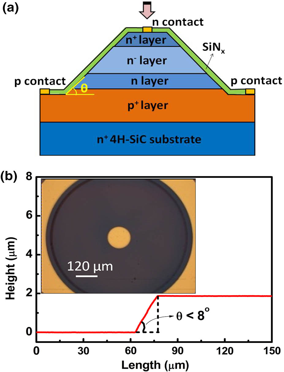
For device fabrication, the epitaxial structure, which was grown on a low-defect-density -type 4H-SiC substrate by metal-organic chemical vapor deposition (MOCVD), consists of a 3 μm layer (), a 0.2 μm n multiplication layer (), a 1 μm absorption layer (), and a 0.3 μm layer (). The device fabrication process started with mesa etching by ion coupled plasma (ICP). In order to suppress the edge breakdown[7], a positive beveled mesa structure () was created. After that, the anode/cathode contact with a metal stack was formed by e-beam evaporation deposition and the standard lift-off technique, which was followed by rapid thermal annealing at 800°C for 3 min in ambient. Then, a 100-nm-thick layer was grown as the passivation layer by PECVD, and the contact area was opened by ICP etching. Finally, the contact process was repeated again with a metal stack for the afterward bonding. The structure of the fabricated 4H-SiC APD is shown in Fig. 1, where the schematic cross-section of the device is plotted in Fig. 1(a), and the profile of the positively beveled mesa is given in Fig. 1(b). Additionally, the top-view image of one 600 μm diameter 4H-SiC APD is provided in the inset of Fig. 1(b).

Figure 1.Structure of our fabricated 4H-SiC APDs. (a) Schematic cross-section of the 4H-SiC APDs; (b) profile of the beveled mesa, where the top-view image of one fabricated 4H-SiC APD with 600 μm diameter is shown in the inset.
As mentioned before, the dark current level is one of the primary limiting factors for scaling the active area of APDs, and the dark current will increase dramatically for large-area SiC APD devices. Therefore, the dark currents of the fabricated large-area 4H-SiC APDs are first characterized and shown in Fig. 2. The dark currents of devices with and without passivation are compared in Fig. 2(a), where the dark current of the sample passivated with conventional is also given. The passivation consists of 20 nm thermally grown and 180 nm deposited by low-pressure chemical vapor deposition (LPCVD). As seen from Fig. 2(a), the dark currents of 4H-SiC APD passivated with both and are reduced by about two orders of magnitude compared with that without passivation, which indicates that the surface or sidewall leakage can be effectively suppressed by passivation as well as the conventional passivation. However, it should be noted that the thermally grown is very time-consuming, while the PECVD passivation can simplify the device fabrication process and save time. Additionally, 4H-SiC APDs with passivation can also enable operation in a harsh environment because of the chemical stability of the material. In order to further verify the suppression of surface or sidewall leakage, the dark currents of fabricated 4H-SiC APDs with different sizes are provided in Fig. 2(b), where the dark current at reverse bias voltage of 120 V is also extracted as a function of device diameter () in the inset. The results show that the dark current is proportional to , indicating that the dark current is dominated by the bulk leakage rather than surface leakage.
Figure 2.Dark current of fabricated large-area 4H-SiC APDs. (a) Comparison of dark current with and without passivation; (b) dark current of fabricated APDs with various sizes.
Furthermore, the UV detection performances of our fabricated 600 μm diameter 4H-SiC APD are characterized. For the first time, to the best of our knowledge, 4H-SiC APDs passivated with instead of are demonstrated in this work. At room temperature, the dark current (), photocurrent () under UV illumination, and the multiplication gain () versus the reverse voltage were measured and calculated, as shown in Fig. 3. The 4H-SiC APD with a large active area shows a low dark current at low reverse bias voltage (), and an abrupt breakdown occurs at the reverse voltage of . The photocurrent is obtained under UV illumination with the wavelength of . With the multiplication gain defined as , and the unity gain defined at the reverse bias of 20 V, the optical multiplication gain of the device is achieved as high as at . Meanwhile, the dark current at the gain of 1000 is just about 2.5 nA (), which is lower than the previously reported results of SiC APDs with an SAM structure[11,12,21].
Figure 3.I–V measurements of the fabricated 4H-SiC APD with 600 μm diameter, where the multiplication gain is calculated.
In addition, the spectral response characteristics and QE of our fabricated large-area 4H-SiC APD at the reverse bias of 120 V were measured under UV illumination, which is depicted in Fig. 4. A peak responsivity of is obtained, corresponding to the external QE of 38.4%. Compared with other reported results, the QE is relatively lower for our samples. This may be caused by several reasons. One possible reason is that the highly doped contact layer in our samples is too thick (0.3 μm), which would degrade the responsivity of APDs due to the so-called “dead space” in the contact layer[8]. Another reason may be that the thickness of the passivation layer is not suitable, as the reflection of light is considered. Therefore, the QE of our 4H-SiC APDs can be further improved by optimizing the thickness of the passivation layer as well as the 4H-SiC epitaxial layers, which will be our ongoing work in the future. For example, the passivation layer in the optical window area can be removed to improve the QE by following the work in Refs. [8,13,14,21].
Figure 4.Spectral response characteristics and external quantum efficiency of fabricated 4H-SiC APD with 600 μm diameter.
Finally, the performance of our fabricated large-area 4H-SiC APD is compared with the reported SiC APDs, as illustrated in Fig. 5. The dark current level and optical multiplication gain are two of the most important performance parameters for APDs. The results show that our 4H-SiC APDs not only have a larger active area but also have comparable high gain and low dark current, which are very important improvements for 4H-SiC APDs with a large active area. The excellent performance is mainly benefited from the high-quality epitaxial material growth and optimized device design as well as the fabrication process. The effective suppression of sidewall leakage current by passivation contributes much to the lower dark current behavior.
Figure 5.Performance of the fabricated large-area 4H-SiC APD compared with the previously reported devices. (a) Comparison of multiplication gain; (b) comparison of dark current at the gain of 1000.
In conclusion, large-area (600 μm diameter) 4H-SiC APDs with SAM structure were fabricated and characterized. A 4H-SiC APD passivated with instead of in our work is demonstrated for the first time, to the best of our knowledge, which indicates that can effectively suppress the surface leakage current, leading to low dark current. At room temperature, our fabricated large-area APDs exhibit comparable performance with the previously reported SiC APD devices, showing high multiplication gain of and low dark current of 2.5 nA () at the gain of 1000.
References
[1] T. Liu, P. Wang, H. Zhang. Chin. Opt. Lett., 13, 040601(2015).
[2] H. Huang, D. Yan, G. Wang, F. Xie, G. Yang, S. Xiao, X. Gu. Chin. Opt. Lett., 12, 092301(2014).
[3] Y. Shi, Z. Li, B. Feng, P. Yan, B. Du, H. Zhou, H. Pan, G. Wu. Chin. Opt. Lett., 14, 030401(2016).
[4] J. C. Carrano, D. J. H. Lambert, C. J. Eiting, C. J. Collins, T. Li, S. Wang, B. Yang, A. L. Beck, R. D. Dupuis, J. C. Campbell. Appl. Phys. Lett., 76, 924(2000).
[5] J. B. Limb, D. Yoo, J. H. Ryou, W. Lee, S. C. Shen, R. D. Dupuis, M. L. Reed, C. J. Collins, M. Wraback, D. Hanser, E. Preble, N. M. Williams, K. Evans. Appl. Phys. Lett., 89, 011112(2006).
[6] H.-D. Liu, X. Guo, D. McIntosh, J. C. Campbell. IEEE Photon. Technol. Lett., 18, 2508(2006).
[7] X. Guo, A. L. Beck, Z. Huang, N. Duan, J. C. Campbell, D. Emerson, J. J. Sumakeris. IEEE Trans. Electron Devices, 53, 2259(2006).
[8] H.-D. Liu, D. McIntosh, X. Bai, H. Pan, M. Liu, J. C. Campbell, H. Y. Cha. IEEE Photon. Technol. Lett., 20, 1551(2008).
[9] H.-D. Liu, X. Zheng, Q. Zhou, X. Bai, D. C. McIntosh, J. C. Campbell. IEEE J. Quantum Electron., 45, 1524(2009).
[10] Q. Zhou, H.-D. Liu, D. C. McIntosh, C. Hu, X. Zheng, J. C. Campbell. IEEE Photon. Technol. Lett., 21, 1734(2009).
[11] Q. Zhou, D. McIntosh, H.-D. Liu, J. C. Campbell. IEEE Photon. Technol. Lett., 23, 299(2011).
[12] X. Cai, D. Zhou, S. Yang, H. Lu, D. Chen, F. Ren, R. Zhang, Y. Zheng. IEEE Photon. J., 8, 6805107(2016).
[13] X. Xin, F. Yan, X. Sun, P. Alexandrove, C. M. Stahle, J. Hu, M. Matsumura, X. Li, M. Weiner, H. J. Zhao. Electron Lett., 41, 212(2005).
[14] J. Hu, X. Xin, X. Li, J. H. Zhao, B. L. VanMil, K.-K. Lew, R. L. Myers-Ward, C. R. Eddy, D. K. Gaskill. IEEE Trans. Electron Devices, 55, 1977(2008).
[15] J. Hu, X. Xin, J. H. Zhao, B. L. VanMil, R. Myers-Ward, C. R. Eddy, D. K. Gaskill. IEEE Trans. Nucl. Sci., 58, 3343(2011).
[16] X. Bai, H.-D. Liu, D. C. McIntosh, J. C. Campbell. IEEE J. Quantum Electron., 45, 300(2009).
[17] D. Zhou, F. Liu, H. Lu, D. Chen, F. Ren, R. Zhang, Y. Zheng. IEEE Photon. Technol. Lett., 26, 1136(2014).
[18] L. Li, D. Zhou, F. Liu, H. Lu, F. Ren, D. Chen, R. Zhang, Y. Zheng. IEEE Photon. Technol. Lett., 28, 2526(2016).
[19] X. Xin, F. Yan, T. W. Koeth, C. Joseph, J. Hu, J. Wu, J. H. Zhao. Electron Lett., 41, 1192(2005).
[20] H.-Y. Cha, S. Soloviev, S. Zelakiewicz, P. Waldrab, P. M. Sandvik. Sensors J., 8, 233(2008).
[21] F. Yan, Y. Luo, J. H. Zhao, G. H. Olsen. Electron Lett., 35, 929(1999).