• Photonics Research
  • Vol. 10, Issue 3, A35 (2022)
Weihong Shen1、2、†, Gangqiang Zhou2、†, Jiangbing Du1、2、*, Linjie Zhou2, Ke Xu3, and Zuyuan He2、3、4
Author Affiliations
  • 1Peng Cheng Laboratory, Shenzhen 518055, China
  • 2State Key Laboratory of Advanced Optical Communication Systems and Networks, Shanghai Jiao Tong University, Shanghai 200240, China
  • 3Department of Electronic and Information Engineering, Harbin Institute of Technology (Shenzhen), Shenzhen 518055, China
  • 4e-mail: zuyuanhe@sjtu.edu.cn
  • show less
    DOI: 10.1364/PRJ.439583 Cite this Article Set citation alerts
    Weihong Shen, Gangqiang Zhou, Jiangbing Du, Linjie Zhou, Ke Xu, Zuyuan He. High-speed silicon microring modulator at the 2 µm waveband with analysis and observation of optical bistability[J]. Photonics Research, 2022, 10(3): A35 Copy Citation Text show less
    Simulation results of the 2 µm MRR under bistability. (a) The calculated output power spectra at different input powers, (b) the hysteresis loop presenting the relationships between output power and input power at a fixed wavelength detuning, (c) power threshold of bistability in a 2 µm ring.
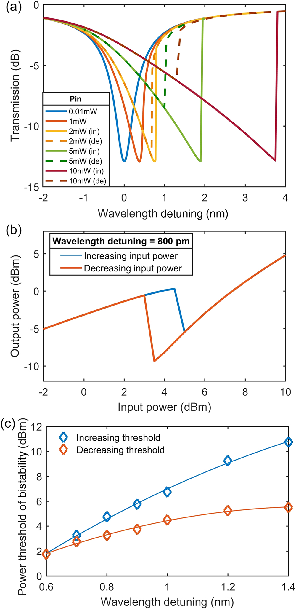
    Fig. 1. Simulation results of the 2 µm MRR under bistability. (a) The calculated output power spectra at different input powers, (b) the hysteresis loop presenting the relationships between output power and input power at a fixed wavelength detuning, (c) power threshold of bistability in a 2 µm ring.
    (a) Microring modulator structure with the N & P implantation regions highlighted. (b) Cross-sectional schematic of the phase shifter in the MRM. (c) Micrograph of the fabricated 2 µm MRM.
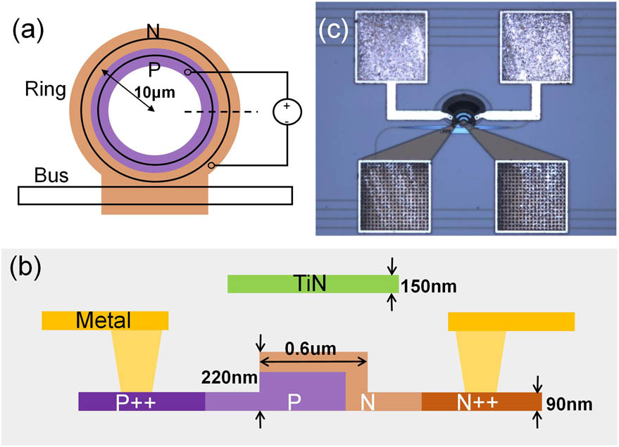
    Fig. 2. (a) Microring modulator structure with the N & P implantation regions highlighted. (b) Cross-sectional schematic of the phase shifter in the MRM. (c) Micrograph of the fabricated 2 µm MRM.
    Simulated carrier concentration of the L-shape phase shifter under reverse biases of (a) 0 V and (b) 2 V.
    Fig. 3. Simulated carrier concentration of the L-shape phase shifter under reverse biases of (a) 0 V and (b) 2 V.
    Experiment setup of the 2 µm MRM.
    Fig. 4. Experiment setup of the 2 µm MRM.
    (a) and (b) The resonant spectrum of the 2 µm MRM, (c) the shifted spectra under different heating powers, (d) the resonance shift as a function of heating power.
    Fig. 5. (a) and (b) The resonant spectrum of the 2 µm MRM, (c) the shifted spectra under different heating powers, (d) the resonance shift as a function of heating power.
    (a) Shifted spectra under different reverse bias voltages measured by thermal sweeping method, (b) the measured S21 frequency responses.
    Fig. 6. (a) Shifted spectra under different reverse bias voltages measured by thermal sweeping method, (b) the measured S21 frequency responses.
    Resonant spectra under different launching powers, measured by the thermal sweeping method.
    Fig. 7. Resonant spectra under different launching powers, measured by the thermal sweeping method.
    Time-domain observation of square waves with 1 MHz and 5 MHz repetition rates under different optical launching power.
    Fig. 8. Time-domain observation of square waves with 1 MHz and 5 MHz repetition rates under different optical launching power.
    Evolutions of ER and SNR of 10 Gbps OOK signal under different launching powers.
    Fig. 9. Evolutions of ER and SNR of 10 Gbps OOK signal under different launching powers.
    (a)–(d) Eye diagrams of 20–35 Gbps OOK signals directly captured on sampling oscilloscope, (e) BER curves of 40 Gbps and 50 Gbps signals with post-FFE eye diagrams.
    Fig. 10. (a)–(d) Eye diagrams of 20–35 Gbps OOK signals directly captured on sampling oscilloscope, (e) BER curves of 40 Gbps and 50 Gbps signals with post-FFE eye diagrams.
    Parameter2 µm RingSource
    n02.3355Calculated
    αring (dB/cm)69Silvaco + Comsol
    Rring (µm)10
    κcoupling0.06Lumerical
    Q2740Calculated
    Aeff (m2)0.35×10¹²Calculated
    ATPA (m2)0.1875×10¹²Calculated
    AFCA (m2)0.166×10¹²Calculated
    n2(m2/W)11×1018[15]
    β2 (m/W)0.2×1011[15]
    κθ (K1)1.78×10⁴[16]
    σFCA,e,p13.22×1020, 1.149[10]
    σFCA,h,q16.21×1020, 1.119[10]
    σFCD,e,p21.91×1021, 0.992[10]
    σFCD,h,q22.28×1018, 0.841[10]
    τcarrier (ps)30
    τphoton (ps)3.15Calculated
    Tthermal (ns)100
    Table 1. Parameters Used in the Simulation of 2 µm Ring
    Weihong Shen, Gangqiang Zhou, Jiangbing Du, Linjie Zhou, Ke Xu, Zuyuan He. High-speed silicon microring modulator at the 2 µm waveband with analysis and observation of optical bistability[J]. Photonics Research, 2022, 10(3): A35
    Download Citation