Weihong Shen, Gangqiang Zhou, Jiangbing Du, Linjie Zhou, Ke Xu, Zuyuan He, "High-speed silicon microring modulator at the 2 µm waveband with analysis and observation of optical bistability," Photonics Res. 10, A35 (2022)
Copy Citation Text
Recently, significantly raised interests have emerged for the 2 µm waveband as an extended new window for fiber optic communication. Much research progress has been made on the photonic integrated circuits for the 2 µm waveband, especially on the CMOS-compatible silicon-on-insulator wafer. In this work, a silicon integrated microring modulator (MRM) with record high-speed performances at the 2 µm waveband was demonstrated. An L-shaped PN junction was specially designed for 2 µm to achieve a high modulation efficiency with of . The measured 3 dB bandwidth is 18 GHz, supporting up to 50 Gbps signaling at 2 µm. Additionally, optical bistability induced by the thermo-optical effect and nonlinear effects was analyzed theoretically and observed experimentally in the 2 µm MRM for the first time to our knowledge. Nonlinear coupled mode theory and the Runge–Kutta method were used to simulate the behaviors of bistability in the 2 µm MRM. The simulation and experimental results indicate that, when the MRM is launched by a high optical power, the distorted resonant spectrum under an optical bistable state deteriorates the modulation efficiency and signal performances. This work breaks the record of high-speed silicon MRM at 2 µm, drawing a promising prospect for the silicon photonic integration and high-speed interconnection at the 2 µm waveband, and it provides the referenceable analysis of optical bistability, which guides the design and experimental investigation of 2 µm MRM.
1. INTRODUCTION
In recent years, in virtue of hollow-core fiber [1] with low loss and low latency, and thulium-doped fiber amplifier (TDFA) [2] with broadband gain, the 2 µm waveband has been considered as a promising communication window apart from the conventional waveband, especially for short-reach optical interconnection and capacity/latency-hungry scenarios like data centers [3,4]. Thanks to the compact footprint and low power consumption, photonic integrated circuits provide a widely used platform for versatile devices. Because of the acceptable absorption loss of silicon at the 2 µm waveband, conventional silicon-on-insulator (SOI) is still a preferred platform for 2 µm waveband integrated devices/systems [5]. Various components for 2 µm, such as tunable arrayed waveguide gratings [6], mode converters [7], and optical switches [8,9], have been fabricated on SOI. As the key role in optical communication systems, electro-optic modulators urgently need to be extended toward longer wavelength for high-speed optical interconnection at the 2 µm waveband. Besides, weaker two-photon absorption and a stronger free-carrier plasma effect on silicon make it more attractive for silicon modulators at the 2 µm waveband [10]. Until now, several silicon modulators at the 2 µm waveband have been reported, such as Mach–Zehnder modulators (MZMs) with a high speed of 80 Gbps [11] and microring modulators (MRMs) with 3 Gbps data rates [12], although, the bandwidth and data rates are still insufficient for high-speed 2 µm waveband transmission. Especially for the MRM, the current modulation bandwidth and efficiency have a large space to be improved.
In addition, two-photon absorption (TPA) effect is an optical nonlinear effect that is easy to generate in silicon under the input optical power on the order of milliwatts (mW). Especially in the MRRs with high power enhancement in the ring, the TPA effect introduces additional nonlinear optical loss and makes a big obstacle for silicon photonics devices in nonlinear application. Optical bistability and self-pulsation can be observed in the microring induced by the thermo-optical effect and several nonlinear effects like TPA and Kerr effects. Besides, as for the optical interconnection system composed of silicon integrated circuits, that may cause the deterioration of transmitted signals and lead to an upper limitation of the high-speed performances.
Compared with the conventional communication band at 1550 nm, silicon at the 2 µm waveband shows lower TPA coefficient, and consequently a weaker TPA effect is expected in the silicon MRR at 2 µm. That will bring some advantages to silicon integrated devices at 2 µm and promote the further development of 2 µm communication. Scant research has been done before on the bistability’s impact on the silicon MRM for high-speed interconnection, and the bistability’s analysis at the 2 µm waveband is still a blank.
In this work, we theoretically analyzed the bistability behaviors in a 2 µm silicon MRM. Based on nonlinear coupled mode theory, nonlinear equations considering the thermo-optical effect and nonlinear effects including TPA, Kerr effect, and carrier dispersion were built up for a 2 µm silicon MRM and solved by the Runge–Kutta method. Based on the silicon 2 µm MRM, the experimental and theoretical analysis of bistability was discussed for the first time to our knowledge. Experimentally, we reported a record high-speed silicon integrated MRM working at the 2 µm waveband, achieving 18 GHz electro-optic bandwidth, high modulation efficiency, and up to 50 Gbps data rates. Bistability behaviors and the deteriorated high-speed performances were captured in the experiment. This work fills the blank of high-speed silicon MRM and the analysis of bistability at the 2 µm waveband, and it shows the promising perspective of the 2 µm waveband on silicon integrated circuits for high-speed optical interconnection.
2. THEORETICAL ANALYSIS OF BISTABILITY IN A 2 μm RING
In a silicon MRR, as input optical power increases, the TPA effect appears in the form of the extra absorption loss of photons and the generation of free carriers. The generated free carriers bring in the free carrier dispersion (FCD) effect and thermo-optical (TO) effect, which present opposite impacts on the refractive index; thus, they shift the resonance wavelength toward the opposite directions. Besides, the difference between free carrier lifetime and thermal decay time results in the diverse response time of FCD and TO effects. Thus, the output power of the MRR becomes much more complicated as the input power and wavelength vary [13]. Two typical behaviors in this case are the bistability and self-pulsation, which present distortions on the resonance spectrum and the time-domain pulse shape, respectively. The bistability mainly manifests as the asymmetric resonant spectrum under high optical launching power, and a hysteresis loop, which we have analyzed by simulation and also observed during the experiment. Self-pulsation presents the quasi-periodical optical oscillating waveforms, the pulse shapes of which vary from different input power and wavelength detuning. Such dynamic process cannot be displayed in the silicon MRM based on free-carrier depletion. That is because the built-in voltage of the PN junction with the reverse bias loaded results in a shorter free-carrier lifetime and breaks the balance between the FCD and TO effects. Therefore, in this work, we only consider and discuss the bistability behaviors of the MRM. In the following numerical simulation, the values of parameters are chosen according to the MRM we designed and fabricated, in order to explain and analyze the behaviors of bistability in a 2 µm ring.
Based on the nonlinear coupled mode theory, the three nonlinear equations, given as follows, describe the temporal evolutions of the intracavity field , free carrier density , and temperature [13]: where is the refractive index of the waveguide, is the resonance frequency of the MRR, is the frequency of incident light, and is the input optical power. The TPA, free carrier absorption (FCA) and FCD, Kerr nonlinearity, and TO effect are taken into account in the nonlinear system, represented by the key parameters of the TPA coefficient , the FCA coefficient , refractive index changed by FCD , the Kerr coefficient , and the TO coefficient , respectively. The changes in absorption coefficient and refractive index induced by free carrier effect can be expressed as follows [10]:
represents the total linear loss of the MRR, including the linear loss in the ring and the coupling loss . consists of the linear material absorption loss, radiation loss of the higher-order mode, sidewall roughness scattering loss, and bending loss. As for the depletion-type MRM, the carrier absorption loss of the PN junction is simplified as a fixed value in this simulation, which is calculated as 69 dB/cm (details of the PN junction are shown in the next section).
The main time-dependent parameters in the nonlinear system are the photon lifetime , free carrier lifetime , and thermal decay time . The photon lifetime is determined by the total loss of the MRR, equivalently the quality factor . Large factor means a high photon lifetime and strong power enhancement in the ring, which consequently reduces the threshold power of bistability. However, it does not mean that bistability cannot occur in a low-Q ring. In this case, photon lifetime is calculated as 3.15 ps, and the factor is 2740, which is consistent with the measured factor of the fabricated device shown in the next section. The free carrier lifetime is mainly affected by the state of silicon–silica interfaces. For the case of depletion-type PN-junction silicon MRM, the carrier lifetime is much shorter than that in an undoped waveguide [14]. Here we simplify as a fixed value of 30 ps, which does not change with the carrier density. The thermal decay time is fixed at 100 ns. Other definitions of the parameters can be found in Ref. [13].
The main parameters used in the nonlinear equations are listed in the Table 1. The parameters related to silicon waveguide, including the mode refractive index and the effective mode areas , , , are calculated by the Eigenmode Solver in Lumerical, modeling the rib waveguides with 220 nm total height, 90 nm slab height, and 600 nm width for the 2 µm waveband. The radius of the 2 µm ring is set as 10 µm, equivalent to the fabricated MRM. The gap between the ring and access waveguide is 290 nm, resulting in a coupling efficiency of 0.06. Hence, the microring works at the uncritical coupling state. Besides, compared to 1550 nm, silicon shows higher Kerr effect, stronger free-carrier dispersion, and weaker TPA coefficient toward longer wavelength at 2 µm [10,15], which makes a difference to the bistability behaviors and shows potential advantages in optical transmission.
Parameters Used in the Simulation of 2 µm Ring
Parameter
2 µm Ring
Source
2.3355
Calculated
(dB/cm)
69
Silvaco + Comsol
(µm)
10
—
0.06
Lumerical
2740
Calculated
()
Calculated
()
Calculated
()
Calculated
[15]
(m/W)
[15]
()
[16]
, 1.149
[10]
, 1.119
[10]
, 0.992
[10]
, 0.841
[10]
(ps)
30
–
(ps)
3.15
Calculated
(ns)
100
–
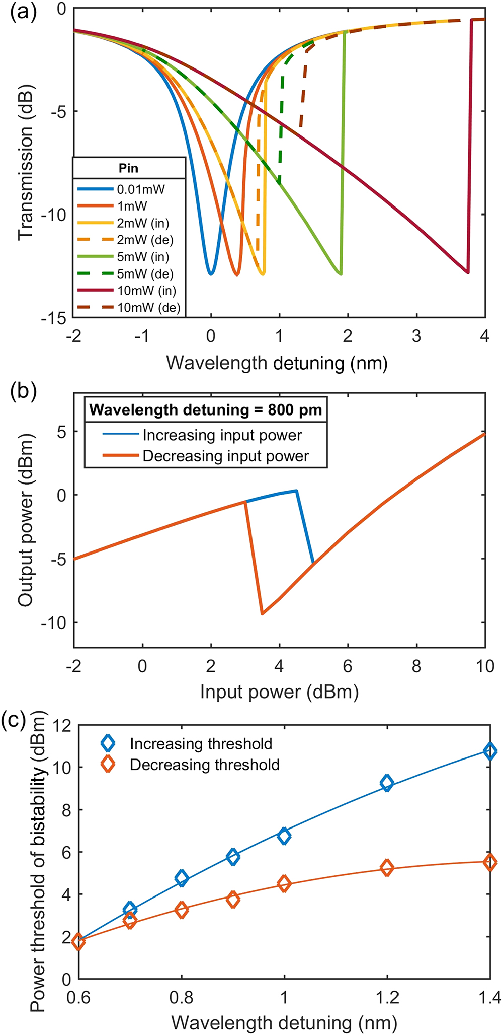
After normalizing the parameters to dimensionless ones, the Runge–Kutta method is applied to calculate the nonlinear equations, and then the normalized parameters are converted back to the real physical values [13]. The simulated results of the 2 µm ring under the influence of bistability are shown in Fig. 1. The results are obtained by solving the nonlinear equations by sweeping the wavelength detuning and input power. As can be seen from Fig. 1(a), the resonant spectrum redshifts with the increasing input power and becomes extremely sharp at the red side, especially when the input power is higher than 2 mW. The solid and dotted lines are results calculated by sweeping the wavelength from blue to red, or in the opposite direction, from red to blue. It is easy to see that the results of dotted lines present lower extinction ratio (ER) at higher input power, which may affect the ER of modulated signals when the ring works as a modulator. The difference between the solid and dotted lines indicates that the intracavity energy is dependent on the previous energy states in the ring. This characteristic can be also presented by the hysteresis loop as shown in Fig. 1(b), which is obtained by sweeping input power in two opposite directions at a fixed wavelength. The output power shows diverse routes as the input power is swept increasingly or decreasingly. At the position of sharp jumping, we can extract the bistability boundary of input power at a certain wavelength, which means the threshold of input power to avoid bistability. The power thresholds at different wavelength detunings are plotted in Fig. 1(c), and the curves of increasing and decreasing threshold define a region of bistability. The power threshold plays an important role in the MRM, which we will discuss by experiment in the next section.
Figure 1.Simulation results of the 2 µm MRR under bistability. (a) The calculated output power spectra at different input powers, (b) the hysteresis loop presenting the relationships between output power and input power at a fixed wavelength detuning, (c) power threshold of bistability in a 2 µm ring.
The silicon 2 µm MRM is fabricated by the MPW run in AMF, Singapore, on the silicon-on-insulator (SOI) wafer with a 220 nm thick silicon layer and a 2 µm thick buried oxide layer. The structure of ring resonator is the same as the mentioned in the former simulation section. As depicted in Fig. 2(b), the phase shifter in the MRM has an L-shaped PN junction. The overlap between the depletion region and optical mode is larger than in a conventional lateral PN junction so as to increase the modulation efficiency [17]. The doping concentrations are , , , and for the N, P, , and doping regions, respectively. The highly doped regions are 700 nm away from the waveguide. The simulated carrier concentrations of the L-shape phase shifter under reverse biases of 0 V and 2 V are depicted in Fig. 3. The PN junction is connected out by aluminum metal lines, and the gap between the metal strips is 10 µm. We applied a 150 nm titanium nitride (TiN) thermal phase shifter to change the resonance wavelength of the MRM.
Figure 2.(a) Microring modulator structure with the N & P implantation regions highlighted. (b) Cross-sectional schematic of the phase shifter in the MRM. (c) Micrograph of the fabricated 2 µm MRM.
For the static characterizations of the 2 µm MRM, a narrow-linewidth fiber laser with fixed wavelength near 1960 nm and an ASE source centered at 1850 nm were employed as the optical sources. The on-chip MRM was coupled from and into fiber via edge couplers with coupling loss at 2 µm. As depicted in Fig. 4, two electrical probes, one DC probe for thermal heating, and one RF probe for high-speed modulation, were applied on the electrodes. Due to the lack of a tunable laser at 2 µm, the operation point of the MRM was tuned by thermal heating voltage via direct current source DC1, shifting the resonance close to the laser wavelength.
By means of ASE source and optical spectrum analyzer (OSA) covering 2 µm, the transmission spectra of resonances are shown in Fig. 5(a) and in the zoom-in spectrum near 1953 nm in Fig. 5(b), showing a free spectrum range of 16.75 nm, full width at half-maximum of 0.94 nm, and extinction ratio (ER) over 15 dB. The fitted factor is 2074, which is slightly different from the simulation result due to the insufficient resolution of the OSA at the 2 µm waveband. Applying the thermal heating power via the DC probe, the resonance near 1953 nm redshifts and gets closer to the wavelength of laser source at 1960 nm as shown in Fig. 5(c). Therefore, the thermal heating power was utilized to control the operation point of MRM for the high-speed transmission in the later section. The resonance shifts are proportional to the heating power, as plotted in Fig. 5(d), with the thermal tuning efficiency of 0.15 nm/mW.
Figure 5.(a) and (b) The resonant spectrum of the 2 µm MRM, (c) the shifted spectra under different heating powers, (d) the resonance shift as a function of heating power.
In order to accurately measure the resonance shifting with the resolution under 0.1 nm, we build up the thermal sweeping method to extract the spectrum by sweeping heating power, instead of sweeping laser wavelength. Single the frequency laser source and power meter at 2 µm were applied in the setup, we swept the thermal heating voltage, recorded the optical power on the power meter automatically at each step, and then used the map of resonance shifts and heating powers shown in Fig. 5(d) to rebuild the spectrum. It is important to note that the redshifting resonance under thermal heating goes across the laser frequency from the blue to the red side; thus, the recovered spectrum by this method is reversed from the real spectrum directly measured by OSA. The shifted resonances under different reverse biases applied on the PN junction are rebuilt by the thermal sweeping method as plotted in Fig. 6(a). The modulation efficiency is 62.1 pm/V, and consequently the product of half-wave voltage and length is 0.85 V·cm, which is improved by nearly 5 times compared with the previous results reported in Ref. [12].
Figure 6.(a) Shifted spectra under different reverse bias voltages measured by thermal sweeping method, (b) the measured S21 frequency responses.
The frequency responses (S21) under various reverse biases are measured by the Agilent 67 GHz vector network analyzer (VNA) as plotted in Fig. 6(b). The 3 dB EO bandwidth is beyond 18 GHz at DC bias, which is currently the record of high-bandwidth MRMs at 2 µm wavelength.
B. Observation of Optical Bistability
By means of the thermal sweeping method mentioned before, we observed the distorted resonance under high launching power. It is clear to see from Fig. 7 that the resonance redshifts as the optical launching power increases and becomes asymmetric due to the launching power higher than 6 dBm (the launching power here refers to the output power of the laser source). These behaviors are highly consistent with the simulation results shown in Fig. 1(a) with wavelength decreasingly swept. At the bistable state, the asymmetric resonance is extremely sharp at the red side, which makes it difficult to control and either operate as a modulator at this wavelength region, while at the blue side, the slope of resonance is slowed down greatly, resulting in the reduction of modulation efficiency. When the launching power reached the maximum of 10 dBm, the resonance also showed a decreased extinction ratio (ER) from 15 to 10 dB, which is consistent with the dotted lines in Fig. 1(a). The decreased ER of resonance results in a worse optical modulation amplitude (OMA) in the high-speed transmission. In the next section, we will discuss the influences introduced by spectrum distortion on the performances of high-speed signals.
Figure 7.Resonant spectra under different launching powers, measured by the thermal sweeping method.
In addition to the distortion of resonant spectrum, bistability also gives rise to the distortion of waveform profiles in the time domain, which should be distinguished from the self-pulsation. Due to the response time of bistability being mainly contributed by the thermal effect, it will not make big difference on the high-speed signals. However, by applying the square electrical waves on the PN junction with repetition rate of several megahertz (MHz), tilted slopes of the “0” and “1” levels of the square wave were observed as shown in the Fig. 8. The received 1 MHz optical waveform at 10 dBm launching power presents a negative slope on “1” level and an opposite slope on “0” level, which reveals the fluctuation of resonance due to the thermal nonlinearities inside the microring. As the repetition rate is increased to 5 MHz, both levels of the square wave present negative slopes, and that is good proof that the response time of bistability is larger than the period of the on–off signal. Thus, the temporal profiles of high-speed signals higher than gigabits per second (Gbps) will not suffer from the bistability, which has been proved in our high-speed transmission system as well.
Figure 8.Time-domain observation of square waves with 1 MHz and 5 MHz repetition rates under different optical launching power.
C. High-Speed Performances Affected by Bistability
As shown in Fig. 4, in the high-speed transmission system, the narrow linewidth laser at 1960 nm was still employed as the optical source. Thermal heating voltage was applied on the DC probe to shift the resonance close to the laser frequency and to control the operation point of the MRM. Pseudorandom binary sequence (PRBS) signals are generated by the arbitrary waveform generator (AWG) with sampling rate of 92 GSa/s and amplified to . The RF signal is combined with DC bias by a bias tee and loaded on the MRM via the RF probe. After the on-chip opto-electronic modulation, the total optical insertion loss is near 18 dB, which includes fiber-to-chip coupling loss. A TDFA was applied to compensate for the large on-chip loss, and then the amplified modulated signals were received by a 20 GHz photodetector (PD) and a real-time oscilloscope (RTO) for offline digital signal processing (DSP) or the digital communication analyzer (DCA) for eye diagram measurement.
In order to observe the bistability’s impact on high-speed performances, we first introduced 10 Gbps on–off keying (OOK) signals onto the MRM. The system settings like the driving voltage, reverse bias, thermal phase shifter, amplifier gain, are all set identical in order to figure out how it will affect the signal performances at high launching power. The measured ERs and signal-to-noise ratios (SNRs) of the 10 Gbps signals are shown in Fig. 9, with the corresponding eye diagrams under different input powers. When the launching power is low, the output power of MRM is lower than , which is a pretty low input value for the amplifier. Thus, TDFA brings in much noise, so the received signal shows a low SNR. As the launching power increases, the SNRs and ERs keep rising, which is straightforward to understand. However, when the launching power increases to 10 dBm, SNR reaches a plateau and is no longer rising, while ER is decreasing. The distorted resonances plotted in Fig. 7 can provide effective proof, in which resonance under 10 dBm launching power shows reduced ER of just 10 dB, so that it leads to the lower ER of signals under the same modulation conditions. This phenomenon indicates that, as the launching power increases to a value that aggravates the bistability, the signal quality will no longer get better; on the contrary, it will get worse. Thus, there exists an optimal launching power, which not only alleviates the ASE noises brought by high-gain TDFA under low input power but also prevents the ER reduction induced by bistability under high launching power.
Figure 9.Evolutions of ER and SNR of 10 Gbps OOK signal under different launching powers.
In a word, considering the optical bistability, silicon MRM with much higher optical launching power may cause the deterioration of high-speed performances and also increase the power consumption. In this case, the threshold power of bistability, or we could say the maximal launching power to avoid bistability, becomes an important value that leads to an upper limitation of signal quality that one can reach only by increasing the launching power. As we mentioned before, compared to 1550 nm, silicon on the 2 µm waveband presents lower TPA coefficient and consequently a weaker TPA effect contributing to the bistability in a silicon 2 µm MRR. Thus, it is reasonable to expect that 2 µm MRM has a much higher threshold power of bistability. In other words, the output power of the optical source could be much higher to generate a better modulated signal with higher SNR at the transmitter side. Although we still need an optical amplifier at the receiver side, due to the insertion loss of the MRM and the fiber-to-chip couplers, the modulated signal has higher power and better SNR before the amplifier; consequently, it shows better signal quality after the amplifier. That illustrates a superior prospect of silicon integrated circuits at 2 µm, especially for the high-speed interconnect systems with hungry power penalty.
D. High-Speed Transmission
After adjusting the operation point of MRM to get rid of the reduction of ER induced by bistability, eye diagrams of 20, 25, 30, and 35 Gbps OOK signals were observed on the sampling oscilloscope as shown in Figs. 10(a)–10(d), appearing with clear open eyes with ERs of 2.659, 2.394, 2.125, and 1.92 dB, respectively. A higher data rate can be achieved by applying a root raised cosine filter and feed-forward equalization (FFE) at the transmitter/receiver side. The bit error rate (BER) curves of the 40 Gbps and 50 Gbps OOK signals are plotted in Fig. 10(e). The 40 Gbps OOK signal has a BER under 7% forward error correction (FEC) threshold () at received optical power, and the 50 Gbps OOK signal shows a BER of at 3 dBm. The corresponding post-FFE eye diagrams are also depicted.
Figure 10.(a)–(d) Eye diagrams of 20–35 Gbps OOK signals directly captured on sampling oscilloscope, (e) BER curves of 40 Gbps and 50 Gbps signals with post-FFE eye diagrams.
In this paper, we have demonstrated a state-of-the-art high-speed silicon integrated microring modulator working at the 2 µm waveband, with 18 GHz bandwidth, high modulation efficiency, and up to 50 Gbps signaling. Considering the thermo-optical and nonlinear effects, optical bistability makes a big difference to the MRM, including the spectrum distortion and deterioration of high-speed signals. The bistability in the 2 µm MRM was numerically analyzed and observed in the experiment. The results reported in this paper provide a guide of the design and experimental investigation of the 2 µm MRM and set a cornerstone of the silicon integrated platform for 2 µm optical interconnection.
References
[1] G. T. Jasion, T. D. Bradley, K. Harrington, H. Sakr, Y. Chen, E. N. Fokoua, I. A. Davidson, A. Taranta, J. R. Hayes, D. J. Richardson, F. Poletti. Hollow core NANF with 0.28 dB/km attenuation in the C and L bands. Optical Fiber Communication Conference, Th4B-4(2020).
[2] Z. Li, A. Heidt, N. Simakov, Y. Jung, J. Daniel, S. Alam, D. Richardson. Diode-pumped wideband thulium-doped fiber amplifiers for optical communications in the 1800–2050 nm window. Opt. Express, 21, 26450-26455(2013).
[3] W. Shen, J. Du, L. Sun, C. Wang, Y. Zhu, K. Xu, B. Chen, Z. He. Low-latency and high-speed hollow-core fiber optical interconnection at 2-micron waveband. J. Lightwave Technol., 38, 3874-3882(2020).
[4] W. Shen, P. Zeng, Z. Yang, D. Xia, J. Du, B. Zhang, K. Xu, Z. He, Z. Li. Chalcogenide glass photonic integration for improved 2 µm optical interconnection. Photon. Res., 8, 1484-1490(2020).
[5] J. Li, Y. Liu, Y. Meng, K. Xu, J. Du, F. Wang, Z. He, Q. Song. 2-µm wavelength grating coupler, bent waveguide, and tunable microring on silicon photonic MPW. IEEE Photon. Technol. Lett., 30, 471-474(2018).
[6] Y. Liu, Z. Li, D. Li, Y. Yao, J. Du, Z. He, K. Xu. Thermo-optic tunable silicon arrayed waveguide grating at 2-µm wavelength band. IEEE Photon. J., 12, 4900308(2020).
[7] S. Zheng, M. Huang, X. Cao, L. Wang, Z. Ruan, L. Shen, J. Wang. Silicon-based four-mode division multiplexing for chip-scale optical data transmission in the 2 µm waveband. Photon. Res., 7, 1030-1035(2019).
[8] J. X. B. Sia, X. Li, Z. Qiao, X. Guo, J. Zhou, C. G. Littlejohns, C. Liu, G. T. Reed, W. Wang, H. Wang. 1 × N (N = 2, 8) silicon selector switch for prospective technologies at the 2 µm waveband. IEEE Photon. Technol. Lett., 32, 1127-1130(2020).
[9] W. Shen, J. Du, K. Xu, Z. He. On-chip selective dual-mode switch for 2-µm wavelength high-speed optical interconnection. IEEE Photon. Technol. Lett., 33, 483-486(2021).
[10] M. Nedeljkovic, R. Soref, G. Z. Mashanovich. Free-carrier electrorefraction and electroabsorption modulation predictions for silicon over the 1–14-µm infrared wavelength range. IEEE Photon. J., 3, 1171-1180(2011).
[11] X. Wang, W. Shen, W. Li, Y. Liu, Y. Yao, J. Du, Q. Song, K. Xu. High-speed silicon photonic Mach–Zehnder modulator at 2 µm. Photon. Res., 9, 535-540(2021).
[12] W. Cao, D. Hagan, D. J. Thomson, M. Nedeljkovic, C. G. Littlejohns, A. Knights, S.-U. Alam, J. Wang, F. Gardes, W. Zhang, S. Liu, K. Li, M. S. Rouifed, G. Xin, W. Wang, H. Wang, G. T. Reed, G. Z. Mashanovich. High-speed silicon modulators for the 2 µm wavelength band. Optica, 5, 1055-1062(2018).
[13] L. Zhang, Y. Fei, T. Cao, Y. Cao, Q. Xu, S. Chen. Multibistability and self-pulsation in nonlinear high-Q silicon microring resonators considering thermo-optical effect. Phys. Rev. A, 87, 053805(2013).
[14] D. Dimitropoulos, R. Jhaveri, R. Claps, J. Woo, B. Jalali. Lifetime of photogenerated carriers in silicon-on-insulator rib waveguides. Appl. Phys. Lett., 86, 071115(2005).
[15] Q. Lin, J. Zhang, G. Piredda, R. W. Boyd, P. M. Fauchet, G. P. Agrawal. Dispersion of silicon nonlinearities in the near infrared region. Appl. Phys. Lett., 91, 021111(2007).
[16] B. J. Frey, D. B. Leviton, T. J. Madison. Temperature-dependent refractive index of silicon and germanium. Proc. SPIE, 6273, 62732J(2006).
[17] G. Zhou, L. Zhou, Y. Zhou, Y. Zhong, S. Liu, Y. Guo, L. Liu, J. Chen. Silicon Mach-Zehnder modulator using a highly-efficient L-shape PN junction. Proc. SPIE, 10964, 1096419(2018).
Weihong Shen, Gangqiang Zhou, Jiangbing Du, Linjie Zhou, Ke Xu, Zuyuan He, "High-speed silicon microring modulator at the 2 µm waveband with analysis and observation of optical bistability," Photonics Res. 10, A35 (2022)