1China University of Mining and Technology, School of Materials and Physics, Xuzhou, China
2Southeast University, State Key Laboratory of Millimeter Waves, Nanjing, China
3Soochow University, School of Physical Science and Technology and Collaborative Innovation Center of Suzhou Nano Science and Technology, Suzhou, China
4Soochow University, Institute for Advanced Study, Suzhou, China
【AIGC One Sentence Reading】:The study realizes strong pseudo-magnetic fields in photonic crystals via gradient deformation, observing quantized Landau levels and unique edge states, paving the way for manipulating electromagnetic wave transport and advancing information processing devices.
【AIGC Short Abstract】:The study realizes a strong pseudo-magnetic field in a two-dimensional photonic crystal via uniaxial linear gradient deformation. This leads to the emergence of Landau level quantization and quantum-Hall-like edge states. By combining reversed gradient photonic crystals, a spatially nonuniform pseudo-magnetic field is achieved, demonstrating the propagation of large-area edge and snake states. This offers a new way to manipulate electromagnetic wave transport and design informative devices.
Note: This section is automatically generated by AI . The website and platform operators shall not be liable for any commercial or legal consequences arising from your use of AI generated content on this website. Please be aware of this.
Abstract
The pseudo-magnetic field, an artificial synthetic gauge field, has attracted intense research interest in the classical wave system. The strong pseudo-magnetic field is realized in a two-dimensional photonic crystal (PhC) by introducing the uniaxial linear gradient deformation. The emergence of the pseudo-magnetic field leads to the quantization of Landau levels. The quantum-Hall-like edge states between adjacent Landau levels are observed in our designed experimental implementation. The combination of two reversed gradient PhCs gives rise to the spatially nonuniform pseudo-magnetic field. The propagation of the large-area edge state and the interesting phenomenon of the snake state induced by the nonuniform pseudo-magnetic field is experimentally demonstrated in a PhC heterostructure. This provides a good platform to manipulate the transport of electromagnetic waves and to design useful devices for information processing.
Many interesting phenomena emerge under the strong magnetic field, for example, the Landau level (LL) and quantum Hall effect.1,2 By artificially introducing the deformation of the graphene lattice by the strain, the Dirac points of the graphene generate a shift in the momentum space, resulting in an effective gauge field of vector potential.3–8 The behavior of electrons in this system is similar to that in a genuine magnetic field; therefore, the synthetic gauge field is called a pseudo-magnetic field (PMF). The PMF leads to quantization of LLs and quantum-Hall-like effects and possesses opposite signs at two inequivalent valleys, so that the time-reversal symmetry is not broken in a system, which provides a new method to control the motion of electrons.
Unlike electronic systems, photons in a photonic crystal (PhC) are uncharged and do not directly couple to an external magnetic field; therefore, various exotic phenomena related to magnetic fields are not accessible in a PhC system (for example, the Aharonov–Bohm effect and Landau quantization). Many works have been studied on how to construct PMFs by using artificial metamaterial in various classical wave systems.9–23 Similar to the strained graphene, for example, the PMF can be generated by the uniaxial or triaxial deformation in sonic crystals10–13 and PhCs.14–21 Different from the perpendicular PMF generated by the shift of Dirac points, many works have been discovered that show the various in-plane PMFs can be obtained by spatially varying mass terms. This synthetic gauge field has been utilized to trap the photonic modes in the photonic Dirac cavity guide,24,25 guide the topological modes in the Dirac waveguide,26,27 and particularly realize the chiral LLs.28
Graphene applied a nonuniform perpendicular magnetic or PMF possesses peculiar properties, such as snake state29–35 and quantum confinement.36 The snake state describes the motion of the trajectory of electrons at the boundary where the magnetic field changes its direction. By analogy to this phenomenon, the snake state has been studied in an elastic wave system.37 However, the nonuniform PMF perpendicular PMF generated by the shift of degenerated Dirac points in the momentum space has not been experimentally demonstrated in a PhC system.
Sign up for Advanced Photonics Nexus TOC. Get the latest issue of Advanced Photonics Nexus delivered right to you!Sign up now
In our work, we theoretically and experimentally realize the uniform and nonuniform PMFs in PhC heterostructures when the uniaxial linear gradient deformation is applied and the lattice symmetry is decreased. The edge state and the snake state in the gap between adjacent LLs are directly observed in the measured distributions of electric fields.
2 Photonic LLs and Edge States
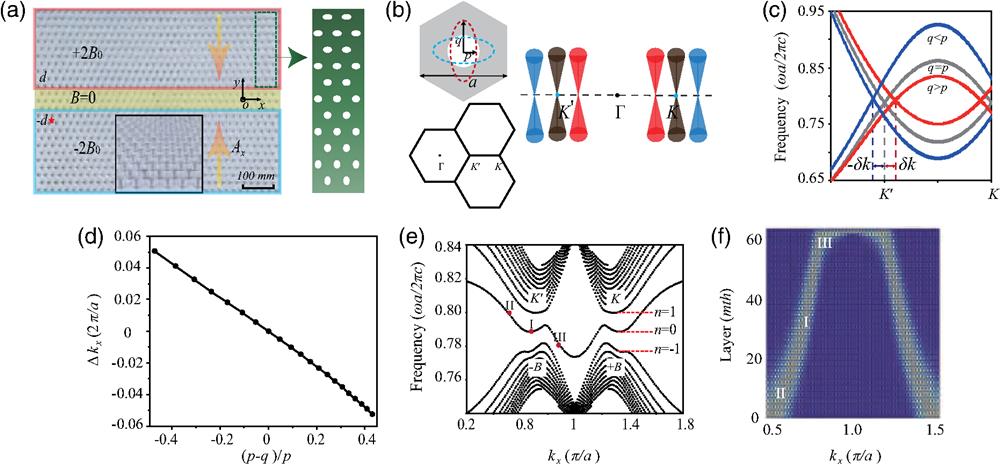
We construct a two-dimensional PhC heterostructure in a spatially nonuniform PMF. The PMFs applied perpendicular to the PhC are constant within each of the three regions, where along the direction is positive, and gives the ratio of two PMFs on the upper and lower regions of a PhC heterostructure. We define the synthetic PMF as when a PhC has 21 layers in the direction. As shown in Fig. 1(a), the upper and lower experimental samples both have 11 layers corresponding to the PMF strength and the parameter . The upper and lower regions of the PhC sample satisfy the mirror symmetry [see the red and blue boxes in Fig. 1(a)]. The uniform PMF in our designed structure is realized in a gradient PhC with a linearly uniaxial deformation along the direction, which uses the same method as Ref. 12. As shown in Fig. 1(b), we first consider a triangular lattice PhC composed of metallic cylinders embedded in the air, in which the lattice constant is and the radius of the cylinder is 4 mm. In the calculated TM ( along the axis) band, degenerated Dirac cones appear at and points [see Fig. 1(c)]. When the filling ratio of the unit cell maintains unchanged and the metallic cylinders are deformed into an elliptical shape, which means the symmetry of the PhC is reduced from to , the Dirac cones shift along the direction in the Brillouin zone, but do not open the bandgap. The two axes of the metallic ellipse are represented by and . The shift of the Dirac cones denoted by has a linear relation with [see Fig. 1(d)] and gives rise to the vector potential .12 As we apply a linear gradient deformation in the direction and translational invariance along the direction, the of th row of the PhC structure is modulated linearly as where and are the length of elliptical pillars at the first and last layers of a gradient PhC, and are fixed as 3.3 and 5.3 mm, respectively, and the number of layers is modulated. Based on the relation between and PMF , the linear variation of causes the PMF along and axes for and valleys in PhCs. Without breaking the time-inversion symmetry, this method can produce similar phenomena caused by external real-magnetic fields. As shown in Fig. 1(e), the Dirac cones at the and valleys become discrete energy level plateaus, where is the LL index, is the photonic analog of the cyclotron frequency, and is the energy level of the Dirac point. The gradient PhC has layers of metallic pillars in the direction and obtains a uniform PMF in Fig. 1(e). The LLs are dispersive in this designed PhC structure, and flatter energy levels can be obtained by tuning the shift of Dirac cones. Therefore, the strong PMF in the gradient PhC leads to the quantization of photonic LLs.
Figure 1.(a) Experimental sample of a heterostructure with nonuniform PMFs, consisting of two reversed gradient PhCs and a transition region. The PMF applied perpendicular to the PhCs is zero in the central yellow region, while has the opposite direction with the same magnitude in the upper and lower half parts. The sign of the PMF is referred to the valley. (b) Left panel: Schematic of the unit cell of the PhC and the Brillouin zone with high symmetry points , , and . Right panel: shift of Dirac cones at and valleys when metallic cylinders are deformed into elliptical shapes. (c) Band structure of the PhC with different sizes of metallic pillars. (d) Linear relation between and the shift of Dirac points represented by . (e) LLs of a gradient PhC under a strong PMF. (f) Distribution of eigen-electric fields of LL and the edge states as a function of wave vector .
We then study the nonuniform PMF in a PhC heterostructure. As displayed in the schematic of Fig. 2(a), the upper and lower parts of the heterostructure have the same 21 layers but the reversed gradient; hence the PMFs of the two parts are antiparallel and the defined ratio at valley. The LLs are dispersive in this structure. Away from the and points, the LLs split into two bands along one direction in the momentum space due to the nonuniform PMF. The bands between adjacent LLs correspond to propagating edge states located at the middle region of the PhC heterostructure. Since the time-reversal symmetry is preserved, the edge states at distinct valleys propagate in opposite directions. The distributions of eigen-electric field at selected points for LL and edge states are shown in the right panels of Fig. 2(a). For the parallel and asymmetric case of corresponding to the combined 21- and 41-layer PhCs, LLs split into two bands along two directions, which become more complicated, and additional bands emerge between adjacent LLs, as shown in Fig. 2(b). We add three layers of metallic cylinders in the middle region as transition layers (PMF is zero) displayed in Fig. 2(c). Here, the number of layers is . The various LLs are deformed, and additional bands indicated by yellow regions correspond to the interesting electromagnetic transport, the so-called “snake state.” The parallel PMFs in the two PhCs cannot cause the snake states as displayed in Fig. 2(d).
Figure 2.(a) Quantization of LLs of two reversed gradient PhCs with layers possessing antiparallel PMFs for . Right panel: distributions of eigen-electric fields. I: LL at and normalized frequency . II and III: edge states at and , . (b) LLs in a heterostructure with the same sign but unequal PMFs. The upper and lower regions have 21 and 41 layers, respectively, for . (c) Snake state in a nonuniform PMFs with layers at each gradient PhC. Right panel: electric field distribution of snake state at and . (d) Dispersive LLs in a heterostructure with parallel PMFs at two PhCs without the snake state dispersion for . Right panel: electric field distribution at and .
The PMF in the PhC leads to the transport phenomenon of edge states, which is similar to the quantum Hall edge state. The energy bands between the different LLs represent the dispersion of the edge states, as shown in Figs. 1(e) and 1(f). The localized edge state at the upper boundary gradually evolves into bulk states distributed in the middle of the structure ( LL) and finally becomes the edge state at the lower boundary near the valley. Here, we experimentally observe the propagation of the edge state. As shown in Fig. 3(a), we place an excited source marked by a red star in the left upper corner of a gradient PhC indicated by the red region. The experimental sample consists of 11 layers of aluminum pillars, and other parameters are the same with the simulations in Fig. 1. The right- (left-) propagating edge state are selectively excited on the top boundary with a positive (negative) group velocity in the simulations and experiments, as shown in Figs. 3(b) and 3(d), corresponding to 10.72 and 10.7 GHz, respectively, between and LLs. The chiral edge state between and LLs spatially distributes at the bottom boundary, shown in Fig. 3(c), which has a large-area distribution of the electric field, in contrast to the localization of edge state on the top side. Owing to the limitation of the scanning field in experiments, the measured area of the electric field is a part of the PhC sample, indicated by a white rectangle in the simulated distribution. An aluminum strip regarded as a perfect electric conductor at the microwave region is placed at the top boundary to prevent the edge state from scattering outside, and other boundaries are clad with absorbing materials. To describe the confinement of the edge state on the top boundary, the parameter is defined as38where is the whole area of the PhCs, denoted by the green dotted box is the edge region as shown in Fig. 3(b), and is the electric field intensity. As shown in Fig. 3(e), the large imply well-localized microwave on the top boundary. The simulated and measured transmission spectra between input and output ports are displayed in Figs. 3(f) and 3(g). The frequency region with high transmission marked by yellow is consistent with the edge state dispersion between and LLs in Fig. 1(e). At LL with 10.78 GHz, the bulk modes are excited, in which electromagnetic waves spread into the central part.
Figure 3.(a) Experimental sample of two reversed gradient PhCs. Red and blue stars indicate the positions of the excited source. (b) and (c) Simulated distributions of electric fields of edge states at the top and bottom boundaries of a gradient PhC, corresponding to 10.72 and 11.0 GHz, respectively. (d) Experimental measurement of the edge state at the top boundary at 10.7 GHz. (e) Defined parameter denotes the confinement of the edge state. (f) and (g) Transmission spectra in the simulation and experiment.
In the nonuniform PMFs constructed by two reversed gradient PhCs, the interface state distributes in the middle domain with a large area displayed in Fig. 2(a), in contrast to the edge states, which are spatially tightly confined on the top boundary of a gradient PhC with the uniform PMF in Fig. 3(b). Hence, it can carry a large amount of energy to design devices, for example, the photonic and acoustic large-area waveguides.39–42 To demonstrate the transport of the large-area interface state, we implement the experiments. The experimental sample is displayed in Fig. 3(a). The excited source is placed at the left of the PhCs marked by a blue star. The four boundaries of the experimental sample are all wrapped with absorbing material. The simulated and experimentally measured electric fields are shown in Figs. 4(a) and 4(b), which indicate that the interface state distributes in the middle domain corresponding to the dispersion between and LLs. The normalized electric field intensity at (560) mm along the direction is shown in Figs. 4(c) and 4(d). The electric field concentrates and distributes uniformly in the middle domain.
Figure 4.(a) and (b) Distributions of the electric field of the large-area interface state in the simulation and experiment at 11.12 and 11.30 GHz, respectively. The measured region of the electric field is a part of the simulated region and PhC sample. (c) and (d) Normalized electric field intensity along the direction at and 560 mm.
At the interface of two domains with opposite magnetic fields, the cyclotron motions of electrons are driven by Lorenz force and present snake-like orbits. By analogy to this interesting transport, the snake state can be achieved in a PhC system. We design a structure composed of two reversed gradient PhCs. The experimental sample is shown in Fig. 1(a), in which the upper and lower parts have 11 layers. Fewer layers lead to a large PMF when the variation of the vector potential is fixed, which means the elliptical pillars at the top and bottom remain unchanged. The PMFs of two gradient PhCs have equal magnitudes but opposite directions. There are three transition layers of the circle pillars placed in the middle of the sample (yellow region), which have zero PMF. The larger transition layers lead to the wider frequency range of the snake state. The excited source is placed at the left of the PhC, as indicated by a red star in Fig. 1(a). The simulated and experimental distributions of the snake states are shown in Figs. 5(a) and 5(b). A disorder is introduced by randomly moving the position of three PhC pillars located at the bend of the wavy trajectory of the electromagnetic waves. The measured electric field demonstrates the propagation of the snake state is unaffected, as shown in Fig. 5(c). However, the transport of the snake state in PMF is fragile when the disorder or defect is introduced on the propagating path, which distinguishes it from the edge state in the quantum spin Hall effect.43,44 The intensity of electric fields at three positions along the direction, as shown in Fig. 5(e), experimentally demonstrates the bending property of the snake state, which agrees with the simulation in Fig. 5(d).
Figure 5.(a) and (b) Electric field distributions of the snake state at 10.42 and 10.30 GHz in the simulation and experiment, respectively. (c) Propagation of the snake state under the disorder realized by moving the position of metallic pillars. (d) and (e) Simulated and experimental electric field intensities along the direction.
The PMF is achieved in a two-dimensional PhC when the lattice remains unchanged and metallic pillars are uniaxially deformed along the direction. A linear gradient PhC has a spatially uniform and strong PMF, which leads to the quantization of LLs and quantum Hall-like edge state confined on a boundary. The nonuniform PMF in a heterostructure composed of two reversed gradient PhCs has a large-area interface state in the middle domain. By adding a transition region with a zero PMF, the snake state arises from the deformed LLs. We implement the experiments to demonstrate the transport of the edge state and snake state. Our proposed structures have unique advantages in obtaining nonuniform PMFs, such as easy implementation, which provides a good platform to observe the manipulation of electromagnetic waves caused by the PMFs.
Bin Yang is currently a master’s student in the School of Materials and Physics at China University of Mining and Technology. His research focuses on photonic crystals and topological insulators under the guidance of Associate Professor Yuting Yang. He strives to advance the theory and explore novel optical phenomena in these fields.
Yuting Yang received her PhD from Soochow University, Suzhou, China, in 2019. During 2018 to 2019, she worked as a visiting PhD student at Nanyang Technological University. She is currently an associate professor in China University of Mining and Technology. Her research interest focuses on topological insulators, photonic crystals, and non-Hermitian topological electric circuits.
Biographies of the other authors are not available.
 AI Video Guide
  AI Picture Guide
 AI One Sentence