1Shenzhen Engineering Laboratory of Phosphorene and Optoelectronics, Key Laboratory of Optoelectronic Devices and Systems of Ministry of Education and Guangdong Province, College of Optoelectronic Engineering, Shenzhen University, Shenzhen 518060, China
2Faculty of Information Technology, Macau University of Science and Technology, Macao, China
3College of Chemistry and Environmental Engineering, Shenzhen University, Shenzhen 518060, China
4School of Materials Science and Energy Engineering, Foshan University, Foshan 528000, China
Black phosphorus (BP), a typical mono-elemental and two-dimensional (2D) material, has gathered significant attention owing to its distinct optoelectronic properties and promising applications, despite its main obstacle of long-term stability. Consequently, BP-analog materials with long-term chemical stability show additional potential. In this contribution, tin sulfide (SnS), a novel two-elemental and 2D structural BP-analog monochalcogenide, has been demonstrated to show enhanced stability under ambient conditions. The broadband nonlinear optical properties and carrier dynamics have been systematically investigated via -scan and transient absorption approaches. The excellent nonlinear absorption coefficient of , 1 order of magnitude larger than that of BP, endows the promising application of SnS in ultrafast laser generation. Two different decay times of ~ and ~ allow the alteration between pure switching and continuous-wave (CW) mode locking in an identical laser resonator. Both mode-locked and -switched operations have been experimentally demonstrated using an SnS saturable absorber at the telecommunication window. Femtosecond laser pulses with tunable wavelength and high stability are easily obtained, suggesting the promising potential of SnS as an efficient optical modulator for ultrafast photonics. This primary investigation may be considered an important step towards stable and high-performance BP-analog material-based photonic devices.
1. INTRODUCTION
Black phosphorus (BP), a typical 2D material, recently has gained significant attention in the communities of electronics and optoelectronics [1–3]. It features a unique layer-dependent direct bandgap [4], which can be adjusted from (bulk) to (monolayer), right filling up the bandgap interval between 0 eV of graphene and large values of transition metal dichalcogenides (TMDCs). The thickness of sensitive direct bandgap is favorable for its optoelectronic applications covering from the near- to mid-infrared spectrum. Recently, a series of investigations revealed that the saturable absorption of BP can span from 0.4 to 2.8 μm, indicating its potential for pulse generation [5]. Lately, BP has also been developed as an optical saturable absorber (SA) for both passively -switched and mode-locked fiber lasers at 1.55 μm with excellent performance [6–8].
Despite these favorable properties of BP, a main drawback is its long-term stability [9]. BP is sensitive to water and oxygen under ambient conditions because of the high activity of phosphorus atoms and the fragile atomic binding [10], resulting in compositional changes and consequent degradation of the electronic and optical performance [11–15]. This severely hinders its applications in flexible electronics, photoelectrons, and electrochemical applications.
To address this drawback, several protection methods have been reported, including covalent bonding with aryl diazonium [16] and carbon free radicals [17], introduction of fluorine adatoms [18], intercalation of alkali metal hydrides [19], metal-ion modification [20], surface coordination of titanium sulfonate ligand [17], and encapsulation by graphene shell [14], hexagonal boron nitride (BN) [11,21], graphene oxide [22], [15,23], organic monolayers, etc. [24]. Although the high stability of BP has been reached, those strategies bring either the advanced synthesis of functional groups or post-treatment of prepared BP nanomaterials, which result in the technical complexity for fabricating BP [25].
Sign up for Photonics Research TOC. Get the latest issue of Photonics Research delivered right to you!Sign up now
A demand for highly stable 2D nanomaterials drives researchers to search for other high-quality BP analog materials with enhanced long-term stability. Fortunately, a group of layered group IV monochalcogenides, such as SnSe [26], GeSe [27], GeS [28], and SnS [29] have puckered structures similar to BP. Bulk SnSe has shown great potential in thermoelectric applications [30,31]. Recently, inspired by the unique property of anisotropic structure in phosphorene, 2D monochalcogenides have attracted great research interest [32–35], especially for their thermoelectric properties [31,36]. Furthermore, compared with the single element in phosphorene, these monochalcogenides are composed of two different types of elements and thus possess different electronegativity [37]. These features can lead to more complicated physics phenomena than that of phosphorene. Indeed, some unique properties, such as giant piezoelectricity [38] and multiferroic with coupled ferroelectricity and ferroelasticity [33,34] have been theoretically proposed. At the same time, experimental investigations on 2D monochalcogenides are in progress [26,39]. SnS exhibits strong anisotropic mechanical and optoelectronic features [37,39–44]. The presence of weak van der Waals force between SnS layers shows no dangling bonds, giving a chemically inert surface [45]. As a result, SnS shows chemical stability even in acidic solution [46], a high melting point of 880°C, and a boiling point of 1230°C. In view of the environment, the Sn and S elements are relatively abundant, and they are safe elements [47]. These favorable properties make SnS a potential material for various applications, including photovoltaics [48,49], solid-state batteries [50,51], thermoelectricity [52], humidity sensors [53], supercapacitor electrodes [54], solar hydrogen production [55], etc.
SnS possesses unique dual direct and indirect bandgaps, with the direct bandgap varying from 1.30 to 1.39 eV and the indirect bandgap from 1.07 to 1.25 eV [42]. In another report, the bandgap of SnS can be adjusted from 1.03 to 1.65 eV [56]. Moreover, it possesses large absorption coefficients (), spanning the ultraviolet to near-infrared (NIR) regions [29,56]. Its carrier mobility was predicted to be tens of thousands of [29], which is even faster than that of BP. Owing to the suitable and tunable bandgap and fast carrier mobility of SnS, excellent nonlinear optical properties can be anticipated. However, investigation of such properties and optoelectronic applications in NIR regions is still in its infancy stage.
In this work, the BP-analog SnS was thus investigated as a new type of effective SA. The high stability of as-prepared SnS nanosheets (NSs) was confirmed through systematic characterizations. Nonlinear absorption was characterized at 800 and 1550 nm, respectively, both exhibiting excellent SA properties. High and tunable modulation depth makes it flexible as a switcher and mode locker. The carrier dynamics, presented by two time components, namely, electron thermalization within the band (873 fs) and recombination of the carriers (96.9 ps), indicates the promising potential of SnS for mode locking. The ultrafast (656 fs) pulse generation in fiber lasers based on SnS NSs was experimentally demonstrated at 1560 nm with high stability. This primary study opens a new avenue for advanced electrophotonics by using BP-analog 2D nanomaterials, suggesting the great promise of group IV monochalcogenides as the substitutions.
2. RESULTS AND DISCUSSION
A. Fabrication and Characterizations
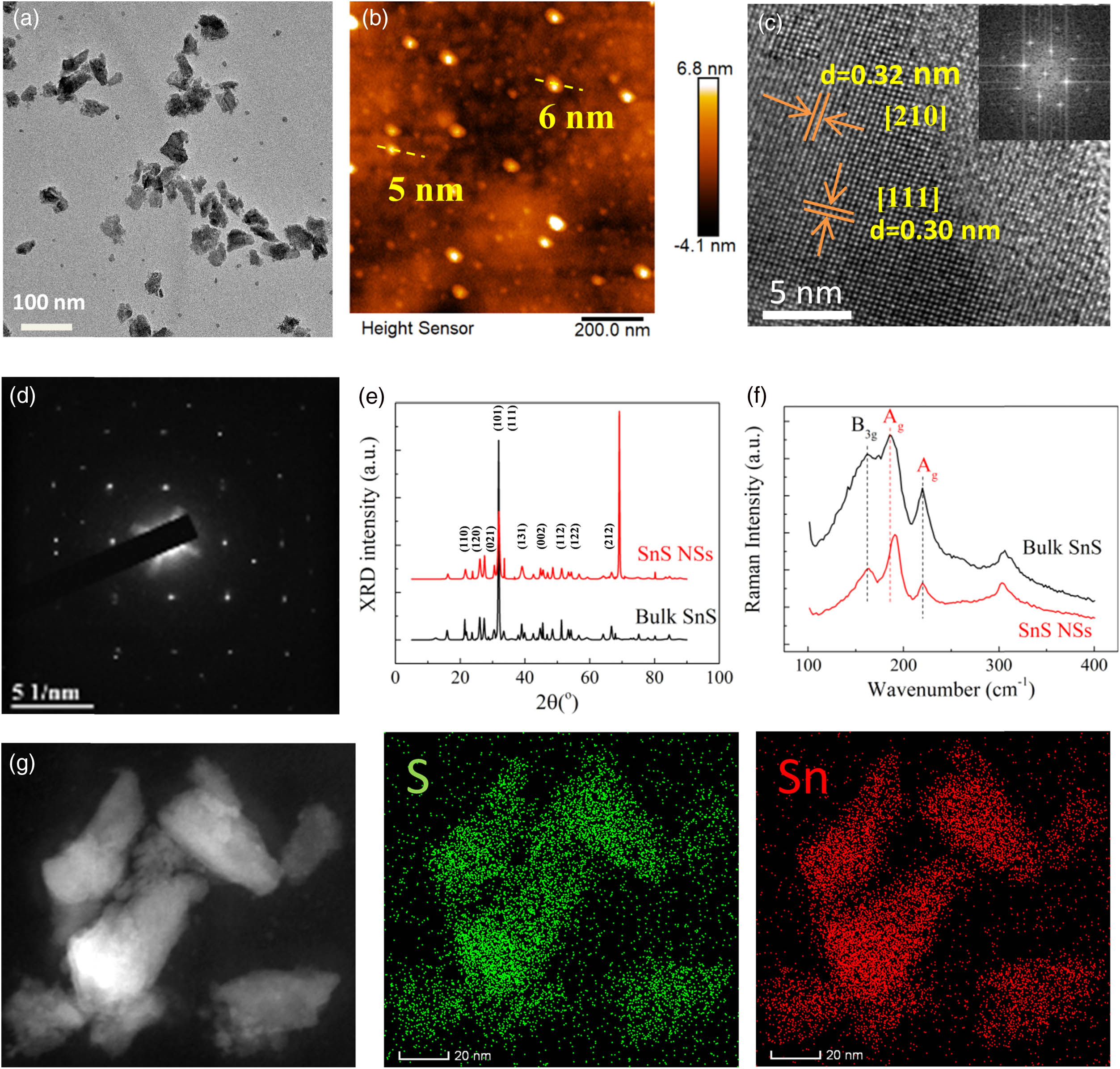
SnS NSs were prepared with the liquid-phase exfoliation (LPE) method. N-methyl-2-pyrrolidone (NMP) was normally chosen to exfoliate SnS [56]. The solvent of isopropyl alcohol (IPA) was chosen to exfoliate SnS in this work because of its lower boiling point, leading to easy removal. In Fig. 1(a), the transmission electron microscopy (TEM) image shows SnS NSs with a main 2D size of and a thickness of less than , as shown by the atomic force microscopy (AFM) image [Fig. 1(b)]. The (210) and (111) planes with interatomic space of 0.32 and 0.30 nm are determined by the observation of high-resolution TEM (HRTEM) [Fig. 1(c)] [57]. Fast Fourier transformation (FFT) of the crystal lattice shows the expected crystallographic lattice reflections [inset of Fig. 1(c)]. The selected-area electron diffraction (SAED) image in Fig. 1(d) suggests that the crystal phase of the SnS NSs remains after the LPE procedure, corresponding to the FFT calculation of the crystal lattice.
Figure 1.Typical characterizations of the SnS NSs. (a) TEM image; (b) AFM image; (c) crystal lattice shown by HRTEM image and corresponding FFT; (d) crystalline features shown by SAED; (e) XRD pattern; (f) Raman spectra of bulk SnS and exfoliated SnS NSs; (g) element distribution mapping via STEM.
The crystal phases of SnS NSs and bulk SnS were compared by employing X-ray diffraction (XRD) and Raman techniques. In Fig. 1(e), both the SnS NSs and bulk SnS exhibited a similar typical XRD pattern. For Raman spectroscopy of bulk SnS, three clear Raman peaks were shown from 100 to . The mode locates at , and the Ag mode is responsible for the peaks at 185.5 and . The peak at comes from owing to the surface oxidation [57,58]. For SnS NSs, the peaks at () and (Ag) indicate a Raman shift compared with the bulk SnS, especially for the Ag mode (from 185.5 to ). It can be concluded that the Ag mode shows the more sensitive layer-dependent behavior in the two vibrational modes because it is along the armchair direction. The energy-dispersive X-ray spectroscopy (EDX) mapping in scanning transmission electron microscopy (STEM) mode presented the composition of Sn and S elements in SnS NSs [Fig. 1(g)]. All measurements determine the composition and crystal phase of the exfoliated SnS NSs.
Concerning the optical applications, the as-exfoliated SnS NSs must possess sufficiently high stability. The stability of SnS NSs was systematically characterized by absorbance spectrum, XRD pattern, Raman spectroscopy, and X-ray photoelectron spectroscopy (XPS). The absorbance of SnS NSs remains stable in 30 days, as shown in Fig. 2(a). Both the XRD pattern and Raman spectrum in 30 days present similar peaks [Figs. 2(b) and 2(c)]. For the XPS characterization [Fig. 2(d)], Sn 3d 5/2 and 3d 3/2 orbitals are responsible for the strong peaks at 485.6 and 494.1 eV, respectively. After 30 days, there was no obvious energy shift. All these characterizations indicate the high stability of SnS NSs in ambient conditions.
Figure 2.Stability of SnS NSs in ambient conditions characterized by (a) absorbance, (b)XRD, (c) Raman, and (d) XPS spectra, respectively.
The steady-state optical response is determined by ultraviolet-visible-near-infrared (UV-vis-NIR) absorption from 350 to 1680 nm, which is measured in IPA solution when the influence of solution has been removed (Fig. 3). From 350 to , the absorbance decreased quasi-linearly, and the absorbance remained almost stable from to . It was interesting to find that there were two absorbance peaks centralized at 1180 and 1480 nm, corresponding to the bandgap of 1.05 and 0.84 eV [Fig. 3(a)]. According to the Tauc plot [Fig. 3(b)], the bandgap of SnS NSs was fitted to be 1.2 eV, similar to the previous report [56]. Therefore, the two above-mentioned absorbance peaks belonged to the subbandgap absorption, which may be caused by crystal defect. These two absorbance peaks strongly suggested that the SnS NSs might be a promising optical material in the telecommunication band.
Figure 3.(a) Linear optical absorption spectrum of SnS NSs from the UV to NIR region in IPA solution. The baseline of IPA has been removed. (b) Corresponding Tauc plot of the linear optical absorption spectrum.
Broadband nonlinear optical absorption of SnS NSs is then characterized by the well-developed -scan technique [5,59]. Under high optical intensity, the total nonlinear absorption could be attributed to various nonlinear absorption mechanisms, including ground state bleaching (GSB), excited state absorption (ESA), two-photon absorption (TPA), and multiphoton absorption (MPA), etc. To characterize nonlinear absorption of few-layer SnS NSs, the transmittance versus the axis was recorded. Strong saturable absorption was observed at both 800 and 1550 nm (Fig. 4). Materials with such significant properties can be used as an efficient optical modulator for switching or mode-locking operations.
Figure 4.Normalized transmittance versus axis at different pulse energies [(a) 800 nm, (c) 1550 nm], and the corresponding intensity-dependent transmittance fitted via a two-level energy model [(b) 800 nm, (d) 1550 nm].
The absorption coefficient of the SnS NSs can be written as where is the linear absorption part, is the nonlinear part ( is the nonlinear absorption coefficient and is the incident optical intensity). The linear absorption coefficient is independent of the optical intensity, which can be obtained at low intensity using the equation , where LT is the linear transmittance (shown in Table 1), and is the length of light path traversing SnS dispersion. is strongly dependent on intensity and can be deduced by fitting normalized transmittance versus axis using the equation [60]where , is the on-axis optical intensity, is the effective propagation length, and is the Rayleigh length. Normalized transmittance versus the pulse energy and the corresponding fitting curves at 800 nm are shown in Fig. 4(a); is fitted to be at the maximum pulse energy of 1.30 μJ. Considering the contribution of third-order nonlinear susceptibility to saturable absorption, the imaginary part of third-order susceptibility (Im ) has a positive correlation with [61], , where is the light speed in vacuum, is the vacuum permittivity, is the linear refractive index ( for IPA solvent [62]), and is the angular frequency of the light. Im is calculated to be at the pulse energy of 1.30 μJ. For 1550 nm, the -scan results and fitting curves are shown in Fig. 4(c), and the corresponding and Im are summarized in Table 1.
LT (%)
ΔT (%)
Tns (%)
Is(GW/cm2)
β(10−3cm/GW)
Imχ(3)(10−21m2/V2)
SnS@800nm
35.9
36.4
27.7
34.8±1.2
−(50.5±3.4)
4.25±0.28
SnS@1550 nm
50.4
12.5
37.1
83.5±2.5
−(14.1±0.3)
2.30±0.05
BP@800 nm
85.6
12.4
1.9
334.6±43
−(6.17±0.19)
—
Table 1. Value of LT, , , , , Im for SnS@800 nm, 1550 nm and BP@800 nm under the pulse energy of 1.3 μJ/pulse and 1.0 μJ/pulse
To further characterize the saturable absorption properties of SnS NSs, the relation between the transmittance and optical intensity [Fig. 4(b)] can be obtained from the -scan results using the equation The transmittance versus the optical intensity can be fitted by a simple saturable absorption model [63]where , , are modulation depth, saturation optical intensity, and nonsaturable loss, respectively. As a BP-analog material, parameters of the SnS are compared with the widely investigated BP [5]. For an SA, higher means the stronger ability to modulate the intensity of the light. A higher value of was calculated to be 36.4% for SnS NSs, compared to other single-elemental 2D materials, including bismuthene (2.03%) [64], antimonene (6.4%) [65], newly found 2D Se (2.13%) [66], as well as BP (12.4%). Additionally, the value of is 1 order smaller than that of the BP, which can help to reduce the threshold of the SA-based mode-locked or -switched lasers. Moreover, the nonlinear coefficient of SnS NSs was found to be larger than that of BP, illustrating the stronger interaction between light and SnS NSs (Table 1). These excellent saturable absorption properties at the communication band mean SnS can be a quite promising candidate as an optical modulator.
C. Characterization of the Relaxation Time
The relaxation time of the charge carriers is a fundamental parameter for semiconductors and significantly affects the performance of that based optoelectronic devices, such as photodetectors, solar cells, and pulsed lasers. The photo-induced carrier dynamics of SnS NSs was investigated with the assistance of a femtosecond-resolved transient absorption (TA) spectrometer. A nondegenerate setup with broad NIR probe band (1000–1500 nm) was employed. Pumped at 400 nm, clearly photon-induced absorption of SnS NSs was observed within the probe band. Figures 5(a) and 5(b) show the TA spectra at the delay line of 0-5.0 ps, which suggests the cooling speed is fast at the beginning, and then becomes slow when the delay line surpasses 5.0 ps. By global time analysis [67], one principal spectrum and kinetic of the charge carrier are figured out, which can well recall the relaxation dynamics [Fig. 5(c)]. is the absorption difference for the probe light with/without the pump light. The electrons are excited to high conduction band in the first 400 fs through the Franck–Condon transition, leaving over the holes in the valence band. The cooling dynamics for SnS NSs can be divided into two processes. Initially, the electrons undergo thermal equilibrium in the conduction band within 873 fs, and then the hot electrons cool down to the valence band and recombine with the holes at 96.9 ps. The probe wavelength-dependent can be fitted using a dual-exponential decay model where is short decay time and is long decay time. In Fig. 5(d), it was observed the short decay time increased from to as the probe wavelength increased from 1000 to 1500 nm, while the long decay time decreased from to . The trend of and means intraband scattering dynamic constant () has a negative correlation with probe wavelength and the interband scattering constant () has a positive correlation with the wavelength.
Figure 5.(a) TA spectra of the SnS sample in the time scale of 0–5.0 ps; (b) 2D mapping of the TA spectrum from 1000 to 1500 nm; (c) principal dynamic figured out by singular value decomposition; (d) decay time and versus the probe wavelength.
Mode locking based on slow SA, that is to say, the pulse width can be smaller than the recovery time, has been proved to be an effective passive technique to generate ultrafast lasers other than the fast SA-like Kerr mode locking for the highly restrictive cavity design. Semiconductor saturable absorber mirrors (SESAMs) [68], and the SA based on recently developed 2D materials, like graphene, TMDs, and BP, enrich the diversity of the slow SA [5,69–71]. For an SESAM, response time associated with the photoinduced electrons and holes relaxation dynamics significantly dominates the performance of the optical devices. It is believed that the short time constant () is the intrinsic character of one kind of material, and the order of hundreds of femtoseconds for SnS materials is suitable for starting the mode locking [72]. While the long time constant (), usually in the time scale from several picoseconds to hundreds of picoseconds, plays an important role in sustaining the mode locking, SnS semiconductor possesses relatively long than graphene and BP [5,69]. Therefore, both mode-locked and -switched operations can be readily realized using the SnS-SA. Moreover, the better chemical stability of SnS over BP shows its potential in pulse laser generation. It is worthwhile to note the contribution of the long decay time of the dynamic process is less than 10%; thus an optical modulation speed as high as terahertz is promised, e.g., gigahertz mode-locking operations.
D. Ultrafast Photonic Applications of SnS NSs
In general, passive switching and mode locking are effective techniques to generate short pulses in bulk lasers. The high-quality SnS-SA facilitates the generation of short and ultrashort pulses by the two techniques. Taking the advantage of the large modulation depth and moderate response time, a passive -switching operation is initially generated from the fiber laser. As described previously [73], there is a critical parameter: , where and represent the saturation energy and modulation depth of the SnS-SA, and is the gain saturation energy of the laser. In the cavity, when the single pulse energy matches the relation of , the switching can be obtained. Otherwise, the continuous wave (CW) mode-locked operation may be achieved. It is worth noting that changing the and with the assistance of adjusting the deposition surface of SnS NSs on microfiber is the convenient way to modify the value of , as is determined by the gain fiber and is hardly modified.
-switched pulses are established when the pump power is increased to 150 mW. However, the pulses cannot be stabilized until the pump power is increased to 275 mW. The pulse repetition rate was 36.36 kHz for 275 mW and increased with the pump power, as Figs. 6(a)–6(e) show. The large scanning range of -switched pulse train in Fig. 6(f) indicates the long-term stability of the -switched state. Besides, once the pump power exceeded 500 mW, the -switched state turned to be unstable again, and the -switched state disappeared. If the pump power exceeded 600 mW, a CW state would be obtained. The evolution of averaged output power and repetition rate as the function of pump power is shown in Fig. 7(a). Both of them increased almost linearly versus the pump power up to 375 mW. The radio-frequency (RF) spectrum of the established -switched pulses at a pump power of 325 mW, giving a high signal-to-noise ratio up to , indicated the extremely stable -switching state.
Figure 6.-switched pulse trains at different pump powers. (a) 275 mW with repetition rate of 36.36 kHz; (b) 300 mW with repetition rate of 38.91 kHz; (c) 325 mW with repetition rate of 41.32 kHz; (d) 400 mW with repetition rate of 49.43 kHz; (e) 500 mW with repetition rate of 65.19 kHz; (f) long-term stability of the -switched state.
Passive CW mode locking is a convenient and effective way to generate ultrashort pulses, demanding the appropriate modulation depth, saturation recovery time, and fine cavity design. Ultrashort and high repetition-rate mode-locked pulses are self-started after carefully adjusting the pump power and optimizing the cavity design. A typical mode-locked state is shown in Fig. 8. The generated pulses are recorded by a 1 GHz-high-speed oscilloscope, showing the fundamental repetition rate of 8.37 MHz, which matches well with the cavity length. A large scanning range of pulse trains at a scale bar of 20 μs shows no fluctuation, proving the stable operation of the mode-locked fiber laser. The mode-locked spectrum of the pulses is centered at and the full width at half-maximum (FWHM) bandwidth is . Clear and distinct Kelly sidebands in the spectrum [Fig. 8(a)], a typical characteristic of the soliton fiber lasers with net anomalous dispersion, indicate that the mode-locked pulses can be shaped into optical soliton pulses. The pulse width was measured to be 656 fs by an intensity autocorrelator, assuming the intensity profile [see Fig. 8(c)]. The calculated time-bandwidth product is , indicating a slight pulse chirp.
The mode-locked laser operates at a highly stable state, for the measured signal-to-noise ratio more than 60 dB from the RF spectrum. To further reveal the long-term stability of mode locking, the mode-locked spectrum at the pump power of 135 mW is recorded over 6 h. No obvious optical spectrum drift was observed [Fig. 9(a)], proving the stable operation.
Figure 9.(a) Long-term operation of SnS NSs-based mode locking and (b) its tunable wavelength.
SnS, as a rising two-elemental and 2D BP-analog group IV monochalcogenide, removes the main obstacle of BP in long-term stability. High-performance 2D SnS was successfully obtained using the LPE method, and its high stability for 1 month has been confirmed by standard and comprehensive characterization techniques. The excellent saturable absorption properties of SnS were found with large and tunable optical modulation depth (maximum value of 36.4%). The saturation optical intensity () is 1 order smaller than that of the BP (), which significantly reduces the threshold of the SA-based pulse lasers. The response time was characterized to be and with the assistance of femtosecond-resolved TA spectra, indicating SnS can be used as a high-speed modulator in the range of gigahertz and even terahertz. Using the SnS as an efficient SA, passive switching and CW mode locking were successfully demonstrated in an identical resonator with high stability. An ultrashort laser pulse sustained for 656 fs was readily obtained. Our systematic study shows that the two-elemental BP-analog SnS is definitely a new type of promising SA, with high stability and robust optical performance compared to single-elemental BP. This could compensate for the main drawbacks of BP and boost the ultrafast photonics of BP-analog materials, such as the group IV monochalcogenides.
Acknowledgment
Acknowledgment. The graduate school at Shenzhen and Tsinghua University Materials and Devices Testing Centre are also gratefully acknowledged.