
Shili Shu, Guanyu Hou, Jian Feng, Lijie Wang, Sicong Tian, Cunzhu Tong, Lijun Wang. Progress of optically pumped GaSb based semiconductor disk laser[J]. Opto-Electronic Advances, 2018, 1(2): 170003
- Opto-Electronic Advances
- Vol. 1, Issue 2, 170003 (2018)
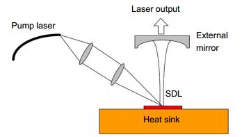
Fig. 1. Schematic of typical SDL cavity
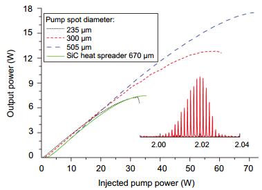
Fig. 2. The output power curves of GaSb based SDL emission at 2.0 μm with different pump spot diameters. Figure reproduced from ref. 16, the Institution of Engineering & Technology.
Fig. 3. Maximum output power of GaSb based SDLs emission at different wavelength operation at 20 ℃.
Fig. 4. Power characteristic of the GaSb based SDL chips with patterned side facets and with cleaved side facets pumped by two different pump spot sizes. Figure reproduced from ref. 10, AIP Publishing.
Fig. 5. Output power of the GaSb based SDLs by using the two gain element structures at heat sink temperature of 20 ℃ with different reflectivity of the output coupling (OC) mirror. Figure reproduced from ref. 20, IEEE.
Fig. 6. Schematic representations of the two main thermal management methods. (a ) Substrate removing; (b ) Intracavity heat spreader.
Fig. 7. 2.0 μm GaSb based SDL with narrow line-width singlefrequency emission. Figure reproduced from ref. 46, IEEE.
Fig. 8. (a ) Optical spectrum together with sech2 fit; (b ) Measured interferometric autocorrelation; (c ) Intensity autocorrelation retrieved from interferometric autocorrelation data and intensity autocorrelation of bandwidth limited pulse computed from spectrum in Fig. 9(a) ; (d ) Pulse shape and Fourier transform limit. Figure reproduced from ref. 51, the Institution of Engineering & Technology.
Fig. 9. Experimental setup and optical measurement arrangement. Figure reproduced from ref. 51, the Institution of Engineering & Technology.
|
Table 1. Heterostructures for GaSb-based SDLs emitting at the range of 2.0~2.8 μm


Set citation alerts for the article
Please enter your email address

© Copyright 2018-2021 | Chinese Laser Press. All Rights Reserved 沪ICP备15018463号-20