• Advanced Photonics
  • Vol. 3, Issue 5, 054001 (2021)
Stefania Castelletto1、* and Alberto Boretti2
Author Affiliations
  • 1RMIT University, School of Engineering, Bundoora, Australia
  • 2Prince Mohammad Bin Fahd University, Deanship of Research, Al Khobar, Saudi Arabia
  • show less
    DOI: 10.1117/1.AP.3.5.054001 Cite this Article Set citation alerts
    Stefania Castelletto, Alberto Boretti. Color centers in wide-bandgap semiconductors for subdiffraction imaging: a review[J]. Advanced Photonics, 2021, 3(5): 054001 Copy Citation Text show less
    CCs and traditional and quantum SRM. (a) Conceptual representation of a vacancy in a wide bandgap semiconductor, giving origin to a three or more levels system made of a ground state (GS) (with spin triplets, depending on the spin number), an excited state (ES), and a metastable state (MS) or intersystem crossing state. (b) The NV and the SiV in diamond are used for SRM methods. (c) 2D hBN showing the boron vacancy. (d) The CAV pairs that can be used for SRM due to their photoswitching properties.59" target="_self" style="display: inline;">59 (e) Traditional SRM methods schematics such as STED, based on depletion of ES via stimulated emission, and SMLM as fully nondeterministic methods, based on the photoswitching of the fluorophore. CSD microscopy originated from the charge conversion of NV from the negative to neutral state, using three laser probes in a more complex approach than STED. STED figure is reproduced from Ref. 60; with permission copyright (2010) John Wiley and Sons, Inc., CSD and Spin-SMLM figures are reproduced from Refs. 48 and 35, under Creative Commons Attribution-NonCommercial-NoDerivs (BY-NC-ND) 4.0 International license. A detailed description of the schematics is provided in the references. (f) Conceptual schematics of the quantum-enhanced SRM developed based on antibunching, giving rise to the mapping of localized single emitters from the spatial imaging of single emitters using a bundle of fibers and array of SPADs and time-correlated single-photon counting (TCSPC).57" target="_self" style="display: inline;">57
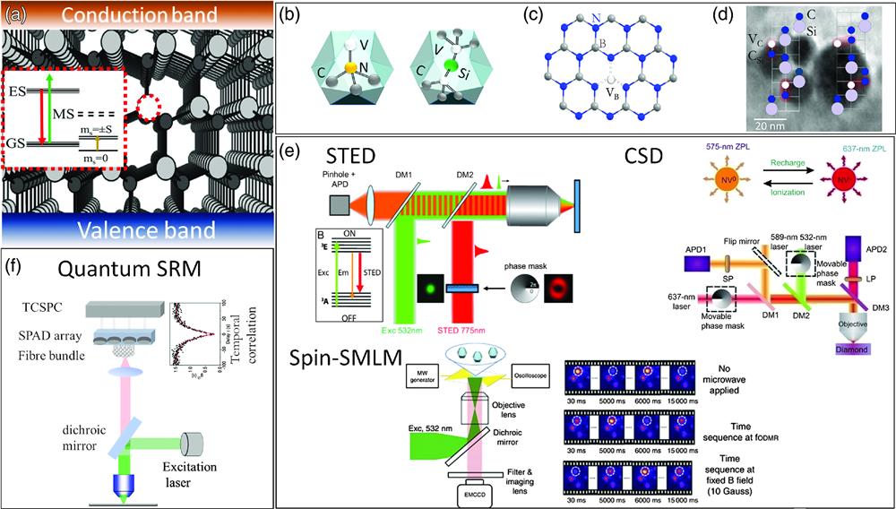
    Fig. 1. CCs and traditional and quantum SRM. (a) Conceptual representation of a vacancy in a wide bandgap semiconductor, giving origin to a three or more levels system made of a ground state (GS) (with spin triplets, depending on the spin number), an excited state (ES), and a metastable state (MS) or intersystem crossing state. (b) The NV and the SiV in diamond are used for SRM methods. (c) 2D hBN showing the boron vacancy. (d) The CAV pairs that can be used for SRM due to their photoswitching properties.59 (e) Traditional SRM methods schematics such as STED, based on depletion of ES via stimulated emission, and SMLM as fully nondeterministic methods, based on the photoswitching of the fluorophore. CSD microscopy originated from the charge conversion of NV from the negative to neutral state, using three laser probes in a more complex approach than STED. STED figure is reproduced from Ref. 60; with permission copyright (2010) John Wiley and Sons, Inc., CSD and Spin-SMLM figures are reproduced from Refs. 48 and 35, under Creative Commons Attribution-NonCommercial-NoDerivs (BY-NC-ND) 4.0 International license. A detailed description of the schematics is provided in the references. (f) Conceptual schematics of the quantum-enhanced SRM developed based on antibunching, giving rise to the mapping of localized single emitters from the spatial imaging of single emitters using a bundle of fibers and array of SPADs and time-correlated single-photon counting (TCSPC).57
    STED applied to FNDs and green FNDs in cells. (a) Scanning confocal image of a BSA-conjugated NV-FND-labeled cell in the white rectangle. (b) STED image of single BSA-conjugated FND enclosed within the green rectangle in (a). (c) Confocal and STED fluorescence intensity profiles of the FND indicated in (b). Solid curves represent the best fits for Gaussian (confocal) or Lorentzian (STED) functions with the FWHM. Images reproduced with permission from Ref. 101, © 2011 John Wiley and Sons, Inc. (d) Superresolution imaging of green FNDs up-taken into an HeLa cell, which is tagged in red with an organic dye. The main image is a confocal scan. The green FNDs appear green, and the absence of fluorescence inside the cells reveals the positions of the nuclei. The two insets are magnified images of the highlighted area of the cell. Scale bars are 5 μm in the main image and 500 nm in the insets. Images reproduced from Ref. 76, © 2015 Optical Society of America (OSA). STED-TEM correlative imaging of intracellular FNDs in TEM sections. (e) A correlation result on a single cell with TEM in gray and fluorescence signal from FNDs in magenta. (f), (g) Zoomed sections of the correlation result for TEM and STED, respectively. (h) The line profile values of an FND in (g), and a two-peak Lorentzian fit of the data with peaks ≈90 nm apart. Images reproduced with permission from Ref. 102, © 2018 John Wiley and Sons, Inc.
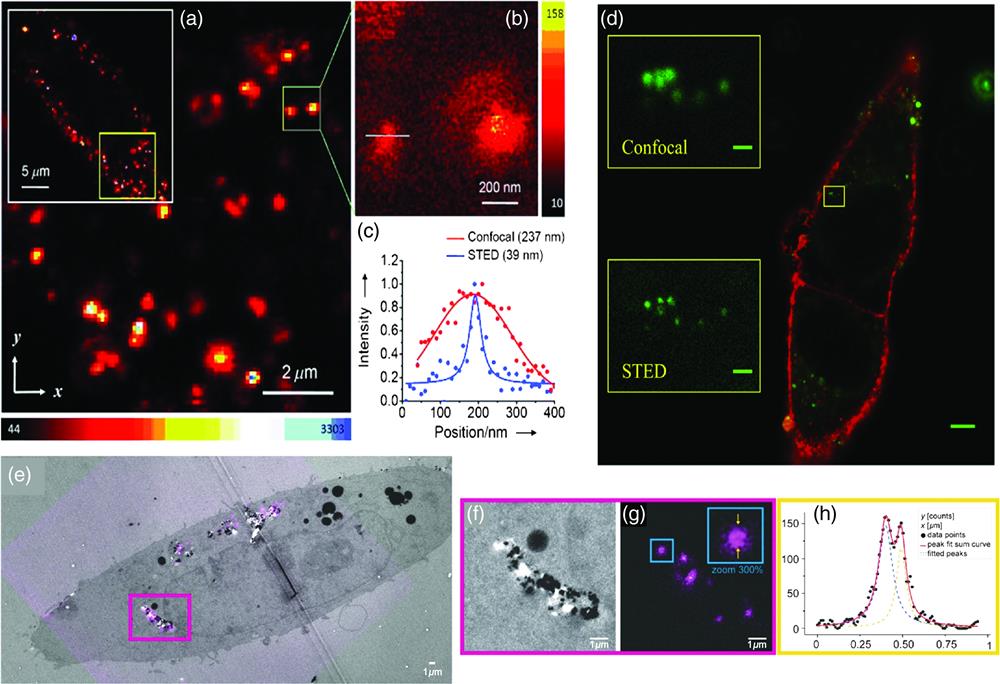
    Fig. 2. STED applied to FNDs and green FNDs in cells. (a) Scanning confocal image of a BSA-conjugated NV-FND-labeled cell in the white rectangle. (b) STED image of single BSA-conjugated FND enclosed within the green rectangle in (a). (c) Confocal and STED fluorescence intensity profiles of the FND indicated in (b). Solid curves represent the best fits for Gaussian (confocal) or Lorentzian (STED) functions with the FWHM. Images reproduced with permission from Ref. 101, © 2011 John Wiley and Sons, Inc. (d) Superresolution imaging of green FNDs up-taken into an HeLa cell, which is tagged in red with an organic dye. The main image is a confocal scan. The green FNDs appear green, and the absence of fluorescence inside the cells reveals the positions of the nuclei. The two insets are magnified images of the highlighted area of the cell. Scale bars are 5  μm in the main image and 500 nm in the insets. Images reproduced from Ref. 76, © 2015 Optical Society of America (OSA). STED-TEM correlative imaging of intracellular FNDs in TEM sections. (e) A correlation result on a single cell with TEM in gray and fluorescence signal from FNDs in magenta. (f), (g) Zoomed sections of the correlation result for TEM and STED, respectively. (h) The line profile values of an FND in (g), and a two-peak Lorentzian fit of the data with peaks 90  nm apart. Images reproduced with permission from Ref. 102, © 2018 John Wiley and Sons, Inc.
    Spin-STED applied to multiple isolated NV− centers in 100 nm ND. (a) Subdiffraction image of five isolated NV centers in a single ND. (b) Vertical STED image profiles as indicated in (a). (c) SEM image of the same ND with (d) the overlay of the STED image. (e) ODMR spectrum of the same NV centers in the same ND showing distinct frequency pairs corresponding to the five NV centers. Reproduced with permission from Ref. 114, © 2013 American Chemical Society (ACS). (f) Spin-RESOLFT experimental sequence combined with AC magnetometry with the dynamical decoupling pulse sequence for quantum sensing using NV centers in diamond. (g) Spin-RESOLFT profiles for a single NV center and different doughnut beam duration with a power of 700 μW. (h) Spin-RESOLFT image of the same NV as in (g) with similar resolution of ≈35 nm but with 25 μW power and a longer duration of 50 μs. Images reproduced from Ref. 115, © 2017 OSA.
    Fig. 3. Spin-STED applied to multiple isolated NV centers in 100 nm ND. (a) Subdiffraction image of five isolated NV centers in a single ND. (b) Vertical STED image profiles as indicated in (a). (c) SEM image of the same ND with (d) the overlay of the STED image. (e) ODMR spectrum of the same NV centers in the same ND showing distinct frequency pairs corresponding to the five NV centers. Reproduced with permission from Ref. 114, © 2013 American Chemical Society (ACS). (f) Spin-RESOLFT experimental sequence combined with AC magnetometry with the dynamical decoupling pulse sequence for quantum sensing using NV centers in diamond. (g) Spin-RESOLFT profiles for a single NV center and different doughnut beam duration with a power of 700  μW. (h) Spin-RESOLFT image of the same NV as in (g) with similar resolution of 35  nm but with 25  μW power and a longer duration of 50  μs. Images reproduced from Ref. 115, © 2017 OSA.
    (a) Schematic of the experimental conditions used to perform GSD nanoscopy applied to hBN flakes with one or two excitation lasers with doughnut-shaped intensity profiles. Here, 532 nm is used as a repumping laser. The direct images and deconvoluted ones are shown in the presence of only the 532-nm or both 532- and 708-nm lasers, together with the resolution achieved, showing an improved resolution in the presence of the two lasers. Images reproduced from Ref. 119, Creative Commons BY license. (b) Schematic representation of GSD microscopy applied to NV− in NDs. Three lasers operating at the wavelengths of 488, 594, and 638 nm are used. The 638-nm laser has a doughnut-shaped intensity profile and switches off the center via the MS state, while the 488-nm laser is a reset beam used to repopulate the ES. Confocal and super-resolved images of 2 NV− at 72-nm distance in the same ND. A single NV was resolved with 36 nm. Images reproduced from Ref. 118, Creative Commons BY license.
    Fig. 4. (a) Schematic of the experimental conditions used to perform GSD nanoscopy applied to hBN flakes with one or two excitation lasers with doughnut-shaped intensity profiles. Here, 532 nm is used as a repumping laser. The direct images and deconvoluted ones are shown in the presence of only the 532-nm or both 532- and 708-nm lasers, together with the resolution achieved, showing an improved resolution in the presence of the two lasers. Images reproduced from Ref. 119, Creative Commons BY license. (b) Schematic representation of GSD microscopy applied to NV in NDs. Three lasers operating at the wavelengths of 488, 594, and 638 nm are used. The 638-nm laser has a doughnut-shaped intensity profile and switches off the center via the MS state, while the 488-nm laser is a reset beam used to repopulate the ES. Confocal and super-resolved images of 2 NV at 72-nm distance in the same ND. A single NV was resolved with 36 nm. Images reproduced from Ref. 118, Creative Commons BY license.
    (a) Spin STORM applied to NV− center in bulk diamond. STORM-ODMR measurement sequence under a 594-nm excitation laser to induce photoionization of the center into its neutral charge state, combined with a scanning of the microwave frequency for each widefield frame. Sensing of two NV− centers is shown with a nanometric localization and STORM-ODMR image. The zero-crossing (line scan) between both centers shows mutual distances of the centers below the STORM resolution. Image reproduced from Ref. 47. (b) Nanoscale magnetic field optical images of labeled cells bound to iron oxide magnetic NPs with biotinylated 70 nm NDs. Upper figures showing super-resolution only based on SMLM using 561 nm and lower figures showing magnetic field sensing and localization combining ODMR information achieved by a microwave frequency scan. Reproduced from Ref. 49, with permission from the Royal Society of Chemistry. (c) Super-resolved image of hBN flakes resolving the different types of emitters (green and red) based on photoswitching of the VB charge states and other emitters in the 2 to 2.2 eV spectral region. Reprinted with permission from Ref. 130, © 2019 ACS. (d) SMLM applied to 4H-SiC NPs of 40 nm after cell incubation achieving 18 nm in the cellular environment. The SiC NPs revealed the presence of multiemitters in the same NP with SMLM using different excitation wavelengths at 561 and 638 nm. Image reproduced from Ref. 59, © 2020 American Physical Society (APS).
    Fig. 5. (a) Spin STORM applied to NV center in bulk diamond. STORM-ODMR measurement sequence under a 594-nm excitation laser to induce photoionization of the center into its neutral charge state, combined with a scanning of the microwave frequency for each widefield frame. Sensing of two NV centers is shown with a nanometric localization and STORM-ODMR image. The zero-crossing (line scan) between both centers shows mutual distances of the centers below the STORM resolution. Image reproduced from Ref. 47. (b) Nanoscale magnetic field optical images of labeled cells bound to iron oxide magnetic NPs with biotinylated 70 nm NDs. Upper figures showing super-resolution only based on SMLM using 561 nm and lower figures showing magnetic field sensing and localization combining ODMR information achieved by a microwave frequency scan. Reproduced from Ref. 49, with permission from the Royal Society of Chemistry. (c) Super-resolved image of hBN flakes resolving the different types of emitters (green and red) based on photoswitching of the VB charge states and other emitters in the 2 to 2.2 eV spectral region. Reprinted with permission from Ref. 130, © 2019 ACS. (d) SMLM applied to 4H-SiC NPs of 40 nm after cell incubation achieving 18 nm in the cellular environment. The SiC NPs revealed the presence of multiemitters in the same NP with SMLM using different excitation wavelengths at 561 and 638 nm. Image reproduced from Ref. 59, © 2020 American Physical Society (APS).
    (a) Schematic of a confocal laser scanning microscope equipped with SPADs and a third-order correlation electronics. (b) Diffraction-limited image from the confocal point of three NV centers in bulk diamond. (c) Map of the g(2) function and super-resolved images using the quantum correlation information after using a quantum reconstruction algorithm for (d) the second-order and (e) third-order. (b)–(e) Images are reproduced with permission from Ref. 55, © 2014 APS. (f) Schematic of an SP fiber bundle camera with 15 SPADs. (g) Photon count time trace (top) and quantum correlation (bottom) for two QDs. Blinking of one QD is followed by antibunching, g(2)(0)≈0, in red. Blue circles correspond to the case of more than one emitter blinking, while gray circles correspond to insufficient statistics. Images (f) and (g) are reproduced from Ref. 163, Creative Commons BY license. (h), (i) Images of microtubules in a fixed 3T3 cell labeled with QDs imaged using ISM and Q-ISM and corresponding SR images (j), (k) for 100 ms and 10 ms acquisition times; the scale bar is 500 nm. Images (h)–(k) are from Ref. 164, © 2019 OSA.
    Fig. 6. (a) Schematic of a confocal laser scanning microscope equipped with SPADs and a third-order correlation electronics. (b) Diffraction-limited image from the confocal point of three NV centers in bulk diamond. (c) Map of the g(2) function and super-resolved images using the quantum correlation information after using a quantum reconstruction algorithm for (d) the second-order and (e) third-order. (b)–(e) Images are reproduced with permission from Ref. 55, © 2014 APS. (f) Schematic of an SP fiber bundle camera with 15 SPADs. (g) Photon count time trace (top) and quantum correlation (bottom) for two QDs. Blinking of one QD is followed by antibunching, g(2)(0)0, in red. Blue circles correspond to the case of more than one emitter blinking, while gray circles correspond to insufficient statistics. Images (f) and (g) are reproduced from Ref. 163, Creative Commons BY license. (h), (i) Images of microtubules in a fixed 3T3 cell labeled with QDs imaged using ISM and Q-ISM and corresponding SR images (j), (k) for 100 ms and 10 ms acquisition times; the scale bar is 500 nm. Images (h)–(k) are from Ref. 164, © 2019 OSA.
    Color centerZPL (nm)η (%)τfl (ns)τISC (ns)σ×1017 (cm2)T2 (μs)
    NV/0 C-bulk637702911.7150×109611.229240062
    NV/0 NDs63723 to 9021.4 to 22.830063680.44 to 1.2769
    SiV/0 C-bulk7380.5701.7822.4714720.035 (T2*)73
    SiV/0 NDs7380.3 to 9.2740.23 to 1.3751200 to 910074n.m.
    NVH NDs5039527,76 40772.1n.m.
    CAV+/016 4H-SiC-bulk648701.840n.a.
    CAV+/0 3C-SiC-NPs176452.1 to 5.3300 to 800n.a.
    DV0/+ 4H-SiC-bulk110014120018,19
    DV0/+ 4H-SiC-NPs781100n.m.
    NCVSi 4H-SiC-bulk791230982.4 to 2.8601 to 68417.2 80,81
    VBCN hBN82,8357165 to 95843.58167 to 833845.5 to 1085n.m.
    VB hBN868501.2287
    Table 1. CCs in diamond, SiC, and hBN flakes with charge states, ZPL, and their optical and spin properties relevant for SRM and quantum enhanced SRM. Specifically, the negative charge state of NV and SiV in diamond, the NVN (H3) center in diamond, the positive CAV pair, the neutral DV in SiC, the negative boron vacancy VB and the complex boron vacancy and carbon–nitrogen antisite VBCN. Properties such as quantum yield (η), fluorescence lifetime (τfl), intersystem crossing lifetime (τISC), stimulated emission cross section (σ), and spin coherence time (T2) are listed. NDs sized 25 to 100 g nm, SiC NPs of 3 to 50 nm. All of the below CCs have been isolated as single emitters except the VB. Here, n.m. stands for not measured and n.a. for not available.
    System (CC)Method (magnetic field sensitivity) (nT/Hz)Resolution (magnetic imaging) (nm)
    NV C-bulkSTED5.8 to 8029
    NV C-bulkSpin-STED (ODMR and Rabi)>10045
    NV C-bulkSIL-STED2.4112
    NV NDsSTED10 to 4032,114
    NV NDsSpin-STED (ODMR)>40114
    NVN C-bulkSTED50106
    NV or NVN NDs in cellsSTED50 to 7076,101
    NV C-bulkCSD4.135
    NV C-bulkSpin-CSD>10035
    NV C-bulkSpin-RESOFLT35 to 50115
    Hahn-echo and magnetic sensing (250)20 to 150115
    NV C-bulkGSD8 to 1631,61
    NV NDsGSD36118
    NV C-bulkSMLM27 to 2947
    NV C-bulkSpin-SMLM (ODMR) (190000)50 to 10047
    NV NDsSuper-resolution radial fluctuations and 2PM43142
    NV NDsSMLM20 to 2333,48
    NV NDsSpin-SMLM (ODMR) (85)17 to 2048
    NV C-bulkSingle photon quantum correlation29055
    SiV C-bulkSTED8972
    hBN few layers flakes VBCN83STED5085
    hBN few layers flakesGSD62119
    hBN monolayer VB83SMLM46129
    SiC 4H CAVSMLM5059
    SiC CAV 4H-NPs in cellsSMLM1859
    Table 2. Super-resolution and their spin variant techniques based on CCs with achieved subdiffraction resolution and magnetic imaging localization resolution and magnetic field sensitivity.
    Stefania Castelletto, Alberto Boretti. Color centers in wide-bandgap semiconductors for subdiffraction imaging: a review[J]. Advanced Photonics, 2021, 3(5): 054001
    Download Citation