
Bao-Jian LIU, Wei-Bo DUAN, Da-Qi LI, De-Ming YU, Gang CHEN, Ding-Quan LIU. The influence of annealing temperature on the structure and optical properties of silicon films deposited by electron beam evaporation[J]. Journal of Infrared and Millimeter Waves, 2020, 39(1): 1
- Journal of Infrared and Millimeter Waves
- Vol. 39, Issue 1, 1 (2020)
Abstract
Introduction
The optical constants of optical thin films, like refractive index and extinction coefficient, are important factors that directly affect the design and preparation of optical thin films. In the Fabry-Perot (F-P) filters, at a given membrane structure, increasing the ratio of the high and low refractive index, can narrow the passband width and expand the cut-off band width[
Some papers concerned the influence of annealing on optical properties and structure of a-Si:H films[
In this paper, the influence of annealing temperature on the structure and optical properties of silicon films was systemically investigated. Silicon films were deposited by electron beam evaporation and then annealed in N2 ambience within 200 ~ 500 °C. The films were characterized by XRD, Raman spectroscopy, ESR and optical transmittance measurement, respectively.
1 Experimental
1.1 Film preparation
Silicon films were deposited by electron beam evaporation on sapphire substrates under identical conditions. Before deposition, the specimens with dimensions of Φ10×1 mm were cleaned with ethyl ether alcohol solution. During silicon films growth, the temperature of substrates was keeping 250°C. The silicon films were deposited by the evaporation rate of 0.4 nm/s at a base pressure of 1×10⁻³Pa. The film deposition time was approximately 45 minutes. After deposition, the samples were annealed for 1h in N2 atmosphere. Annealing temperatures were 200°C, 300°C, 400°C and 500°C, respectively. The temperatures were heightened to desired level gradually.
1.2 Film characterization
The X-ray diffractometer (XRD) was wielded to investigate the structure of silicon films by Cu-target Kα radiation at 40 kV in the scanning angular from 10° to 80° at 2°/min. The Raman spectra were acquired to estimate the evolution of network structure through Micro Raman Spectrometer with the HeCd laser beam at 532 nm. The ESR measurement was performed by a double-cavities BRUKER ESP4105 spectrometer operated by X-band microwave radiation with a power of 20 mW at 80 K. Via a Lambda 900 spectrophotometer, the transmission spectrum of silicon films were measured and the measurement error was within 0.08%. From transmittance spectra, the refractive index (n) and extinction coefficient (k) of silicon films were calculated by using the Cauchy Exponential Model. In the dispersion model, the absorption coefficient varied exponentially with frequency. This allowed the Cauchy Exponential to model a large variation in the value of k versus wavelength. The following formulas were used to define the optical constants[
where λ is wavelength, An, Bn, and Cn are material coefficients, Ak is amplitude, Bk is the exponent factor and Ck is the band edge.
2 Results and discussion
2.1 Structure of silicon films
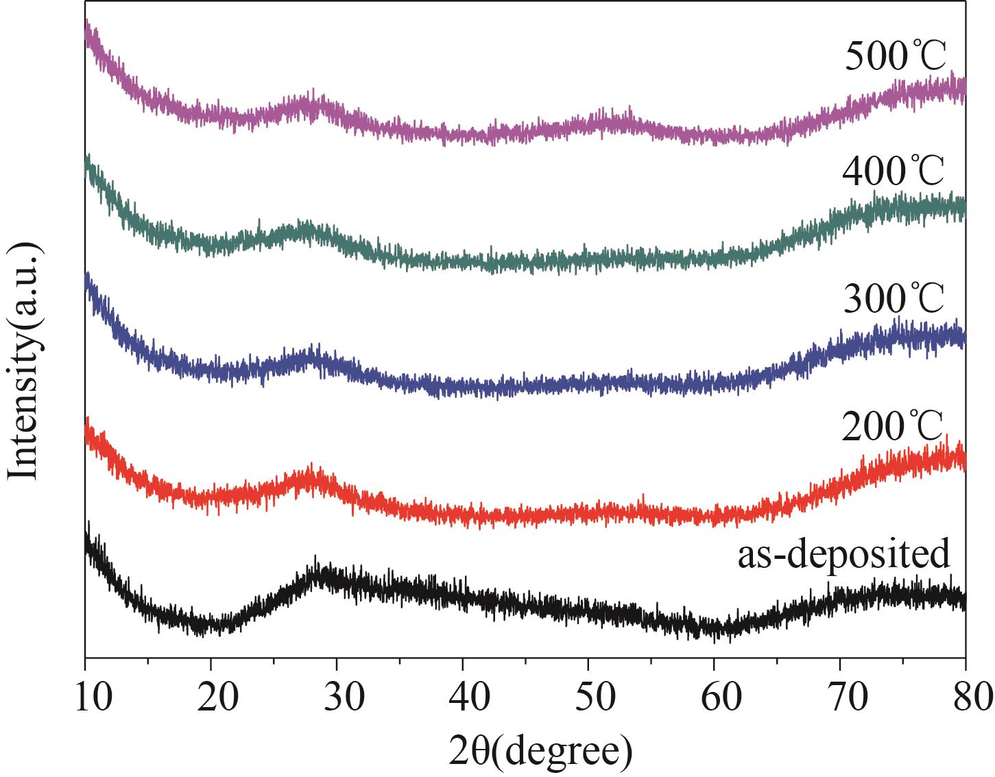
As shown in
![]()
Figure 1.XRD patterns of silicon films annealed at different temperatures.
The widespread usage of Raman scattering into the research of microstructure materials lied in the fact that its intensity was susceptible to the order degree of solid structure. The Raman spectra of as-deposited and annealed silicon films were shown in
![]()
Figure 2.(a) Raman spectra of the as-deposited and annealed silicon films; (b) The Gauss-deconvolution of Raman spectrum for silicon film annealed at 400 °C.
| Annealing temperature (°C) | ГTO(cm-1) | ILA/ITO | ILO/ITO | ITA/ITO |
|---|---|---|---|---|
| as-deposited | 68.4 | 1.02 | 0.358 | 0.670 |
| 200 | 67.4 | 0.718 | 0.352 | 0.592 |
| 300 | 66.7 | 0.711 | 0.334 | 0.524 |
| 400 | 66.4 | 0.678 | 0.331 | 0.481 |
| 500 | 65.9 | 0.690 | 0.350 | 0.478 |
Table 1. Raman characteristic parameters of the as-deposited and annealed silicon films
ESR was among few experiments offered defects information in structure[
![]()
Figure 3.Derivative ESR spectra of the as-deposited and annealed silicon films
![]()
Figure 4.Optical transmittance spectra of as-deposited silicon film and the silicon films annealed at different temperatures.
![]()
Figure 5.Variation of film optical thickness and physical thickness with annealing temperatures.
The optical constants of silicon films were fitted by using the FilmWizard software from SCI. During fitting process, the Cauchy Exponential Model was used as the dispersion model of material to fit the transmission spectrum.
| Annealing temperature (°C) | An | Bn | Cn | Ak | Bk | Ck |
|---|---|---|---|---|---|---|
| as-deposited | 3.322 | 0.143 | 0.059 | 4.088×10⁻⁵ | 4.858 | 0.228 |
| 200 | 3.304 | 0.124 | 0.068 | 1.349×10⁻⁵ | 5.680 | 0.229 |
| 300 | 3.293 | 0.112 | 0.073 | 1.328×10⁻⁶ | 7.117 | 0.232 |
| 400 | 3.302 | 0.111 | 0.074 | 4.136×10⁻⁷ | 7.861 | 0.245 |
| 500 | 3.386 | 0.119 | 0.076 | 8.843×10⁻⁷ | 7.509 | 0.271 |
Table 2. Dispersion model parameters of the as-deposited and annealed silicon films
![]()
Figure 6.Dispersion of (a) refractive index,(b) extinction coefficient of the as-deposited and annealed silicon films
3 Conclusion
The silicon films were deposited on sapphire wafer by electron beam evaporation and then annealed in N2 atmosphere in a temperature range from 200 to 500 °C. It was concluded that all silicon films maintained amorphous in microstructure, but with annealing temperature increased, the amorphous network order was improved on the short and medium range. Meanwhile, the defect concentration from ESR measurement decreased distinctly. When sample being annealed at 400°C, the defect density declined to the minimum, about one fifth of the as-deposited sample. With annealing temperature increased, transmittance spectra of silicon films shifted to the shorter wavelength direction, owing to the decrease of film thickness and the change of refractive index. When sample being annealed at 400°C, extinction coefficient also cut down to the minimum, and then mounted up by rising annealing temperature further. According to these results, annealing at an appropriate temperature could effectively reduce the optical absorption of silicon films in the near infrared region, which were very critical for the application in optical thin film coating devices.
References
[1] S Bruynooghe. 48. Applied optics, 47, C47(2008).
[2] H Yoda, K Shiraishi, Y Hiratani. a-Si:H/SiO2 multilayer films fabricated by radio-frequency magnetron sputtering for optical filters. Applied optics, 43, 3548-3554(2004).
[3] L Mao, H Ye. New development of one-dimensional Si/SiO2 photonic crystals filter for thermophotovoltaic applications. Renewable Energy, 35, 249-256(2010).
[4] I S Gainutdinov, E A Nesmelov, R D Aliakberov. Stabilization of the optical parameters of filters based on amorphous silicon. Journal of Optical Technology, 71, 842-846(2004).
[5] C S Long, H H Lu, D F Lii. Effects of annealing on near-infrared shielding properties of Cs-doped tungsten oxide thin films deposited by electron beam evaporation. Surface & Coatings Technology,, 284, 75-79(2015).
[6] S H Woo, C K Hwangbo. Effects of annealing on the optical, structural, and chemical properties of TiO2 and MgF2 thin films prepared by plasma ion-assisted deposition. Applied optics, 45, 1447-1455(2006).
[7] A F Khan, M Mehmood, A M Rana. Effect of annealing on structural, optical and electrical properties of nanostructured Ge thin films. Applied Surface Science, 256, 2031-2037(2010).
[8] M Zarchi, S Ahangarani. Study of silicon films deposited by EB-PVD and the effect of applying annealing conditions on them. Optik,, 154, 601-609(2018).
[9] N Elghoul, S Kraiem, R Jemai. Annealing effects on electrical and optical properties of a-Si:H layer deposited by PECVD. Materials Science in Semiconductor Processing, 40, 302-309(2015).
[10] X N Wang, X Y He, W F Mao. Microstructure evolution of amorphous silicon thin films upon annealing studied by positron annihilation. Materials Science in Semiconductor Processing,, 56, 344-348(2016).
[11] G B Tong, M R Muhamad, S A Rahman. Optical properties of annealed Si:H thin film prepared by layer-by-layer(LBL) deposition technique. Physica B, 405, 4838-4844(2010).
[12] M Netrvalová, V Vavruňková, J Müllerová. Optical properties of re-crystallized polycrystalline silicon thin films from a-Si films deposited by electron beam evaporation. Journal of Electrical Engineering, 60, 279-282(2009).
[13] H Fujiwara. Spectroscopic Ellipsometry: Principles and Applications(2007).
[14] M S Amin, N Hozhabri, R Magnusson. Effects of solid phase crystallization by rapid thermal annealing on the optical constants of sputtered amorphous silicon films. Thin Solid Films, 545, 480-484(2013).
[15] J He, C Wang, W Li. Effect of gas temperature on the structural and optoelectronic properties of a-Si:H thin films deposited by PECVD. Surface & Coatings Technology, 214, 131-137(2013).
[16] M Marinov, N Zotov. Model investigation of the Raman spectra of amorphous silicon. Physical Review B, 55, 2938-2944(1997).
[17] W S Wei, G Y Xu, J L Wang. Raman spectra of intrinsic and doped hydrogenated nanocrystalline silicon films. Vacuum, 81, 656-662(2007).
[18] N Zotov, M Marinov, N Mousseau. Dependence of the vibrational spectra of amorphous silicon on the defect concentration and ring distribution. Journal of Physics Condensed Matter,, 11, 9647-9658(1999).
[19] R A Street. Hydrogenated Amorphous Silicon(1991).
[20] O Astakhov, R Carius, A Lambertz. Structure of the ESR spectra of thin film silicon after electron bombardment. Journal of Non-Crystalline Solids, 19, 2329-2332(354).

Set citation alerts for the article
Please enter your email address
© Copyright 2018-2021 | Chinese Laser Press. All Rights Reserved 沪ICP备15018463号-20