Jianmiao Zhang, Feng Jin, Xianzi Dong, Meiling Zheng. China' s Top 10 Optical Breakthroughs: Laser Fabrication and Applications of 3D Inorganic Micro and Nanostructures (Invited)[J]. Laser & Optoelectronics Progress, 2024, 61(19): 1900001
Search by keywords or author
- Laser & Optoelectronics Progress
- Vol. 61, Issue 19, 1900001 (2024)
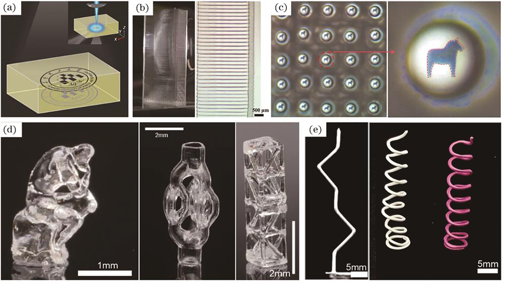
![Continuous wave (CW) laser fabrication of 3D inorganic micro and nanostructures. (a) 473 nm CW laser writes patterning information in glass [3]; (b) photograph of 105 layers glass structure processed by CO2 laser (left), optical microscope image of sidewall section (right) [39]; (c) glass microlens array processed by CO2 laser, the image on the right is the image effect of a single microlen[40]; (d) 3D transparent glass microstructures processed by 442 nm CW laser[41]; (e) unsupported ceramic microstructures fabricated by 980 nm CW laser [42]](/richHtml/lop/2024/61/19/1900001/img_01.jpg)
Fig. 1. Continuous wave (CW) laser fabrication of 3D inorganic micro and nanostructures. (a) 473 nm CW laser writes patterning information in glass [3]; (b) photograph of 105 layers glass structure processed by CO2 laser (left), optical microscope image of sidewall section (right) [39]; (c) glass microlens array processed by CO2 laser, the image on the right is the image effect of a single microlen[40]; (d) 3D transparent glass microstructures processed by 442 nm CW laser[41]; (e) unsupported ceramic microstructures fabricated by 980 nm CW laser [42]
![Picosecond laser fabricating 3D inorganic micro and nanostructures. (a) Picosecond laser welding ceramic components[44]; (b) end face of damaged channel[46]; (c) picosecond laser embedded 3D structure in transparent glass[47]; (d) 3D microstructure of glass fabricated by picosecond laser fabricating HSQ[51]](/richHtml/lop/2024/61/19/1900001/img_02.jpg)
Fig. 2. Picosecond laser fabricating 3D inorganic micro and nanostructures. (a) Picosecond laser welding ceramic components[44]; (b) end face of damaged channel[46]; (c) picosecond laser embedded 3D structure in transparent glass[47]; (d) 3D microstructure of glass fabricated by picosecond laser fabricating HSQ[51]
Fig. 3. Femtosecond laser fabrication of 3D inorganic micro and nanostructures in glass. (a) Permanent trace in glass[54]; (b) femtosecond laser writes low loss curved waveguide in glass[56]; (c) patterning of femtosecond laser inside Au doped glass[62]; (d) femtosecond laser writing of depth information in glass[64]; (e) CsPbBr3 nanocrystalline structures prepared by femtosecond laser[65]; (f) femtosecond laser writing 3D inorganic microstructure based on HSQ[69]
Fig. 4. Femtosecond laser fabricating 3D inorganic micro and nanostructures in optical crystal. (a) End view of concave cladding waveguide written in YAG∶Nd3+ [70]; (b) waveguide end face written in LiNbO3 crystal[74]; (c) cross section of waveguide in ZnS crystal[71]; (d) double line (No.1) and concave cladding (No.2) waveguides generated in LBO crystal[73]; (e) nanoscale regulation of femtosecond laser in LiNbO3 crystal[78]; (f) femtosecond laser writes holograms of specific patterns in LiNbO3 crystal[80]
Fig. 5. Femtosecond laser fabrication of 3D inorganic micro and nanostructures based on ceramics and quantum dots. (a) Femtosecond laser-induced chemical bonding of quantum dots to form 3D inorganic micro and nanostructures[32]; (b) femtosecond laser printing of mixed quantum dots to form a 3D nanopillar array[81]; (c) femtosecond laser fabricating circular waveguides in ceramics with spiral motion[84]
Fig. 6. Femtosecond laser fabricating of 3D inorganic micro and nanostructures in precursor photoresist containing inorganic components. (a) Self supporting aspheric microlens [85]; (b) tetrahedral cell [86]; (c) free form sculpture [87]; (d) micron cross torsion structure [88]; (e) drying shrinkage process causes 3D structural cracks [89]; (f) porous microchannel structure [90]; (g) microlens printed on support column [91]; (h) 150 μm-high diffractive micro objective lens[33]
Fig. 7. Femtosecond laser fabrication of 3D inorganic micro and nanostructures based on inorganic nanoparticles doped photoresists. (a) Transparent glass microstructure[92]; (b) pendant [93]; (c) disk truss structure (left) and octahedral truss structure (right)[94]; (d) ceramic lattice cube [95]
Fig. 8. 3D inorganic micro and nanostructures prepared by the polymer template assisted femtosecond laser fabrication method. (a) Alumina octahedral truss nanolattice[97]; (b) microstructure of DNA double helix hollow glass[10]; (c) 3D silicon nanostructure[98]; (d) double-well ceramic nanolattice[99]; (e) 3D hollow spiral microtubule structure[100]
Fig. 9. Application of 3D inorganic microstructure as optical micro devices. (a) Microring optical resonator[94]; (b) glass microlens[92]; (c) Alvarez lens[2]; (d) Fresnel lens[69]; (e) photonic micro ring resonator[51]; (f) plano convex microlens with aspheric profile[33]
Fig. 10. Laser fabrication of 3D inorganic micro and nanostructures for quantum chips. (a) Femtosecond laser patterns resistors[102]; (b) femtosecond laser directly writing optical waveguide (left) and waveguide directional coupler (right)inside the glass[104]; (c) femtosecond laser direct writing 3D waveguide array (top left), photonic lattice section (bottom left), schematic diagram of coupling one waveguide to other waveguides in a 3D waveguide array (upper right), and evolution pattern of single photon output after quantum walk in the lattice (lower right)[106]; (d) 3D layout of three qubit Toffoli gate encoded by femtosecond laser direct writing path[107]
Fig. 11. Application of laser fabricated 3D inorganic micro and nanostructures. (a) Femtosecond laser erasure/recovery[66]; (b) QR code encryption demonstration[67]; (c) patterning of Cl-Br-—I- codoped glass[65]; (d) side view of laser welding[112]; (e) assembly drawing of successful laser welding[44]; (f) vertical waveguide in the sensor[7]; (g) microstructure of storage bin[115]; (h) fabrication of fused quartz by circularly polarized laser pulses[117]; (i) effect comparison between bare quartz glass and quartz glass with anti-reflective structure[118]; (j) truncated cone array [119]

Set citation alerts for the article
Please enter your email address


